

Page 1
User Guide 083
ISL76534EVAL1Z Evaluation Board User Guide
Description
The ISL76534EVAL1Z is a complete platform for the
evaluation on all datasheet specifications and functionalities
of the programmable gamma buffer. The ISL76534
I2C programmable, 10-bit, 14-channel gamma reference
voltage generator with buffered outputs, a 10-bit programmable
calibrator, a high output current V
V
COM
internal EEPROM to store all reference voltage data. The
EEPROM features an endurance of 10,000 write cycles and a
data retention of 20yrs at 105°C.
The ISL76534EVAL1Z board is intended to provide an
evaluation platform for the 4mmx5mm X2QFN
package, programmable gamma buffer.
COM
contains an
amplifier and an
ISL76534
Specifications
• Ambient temperature range, -40°C to +105°C
VDD
COM
VDD
= 0V to A
= 6.3V to 19V
= 2.25 to 3.6V
-Headroom
VDD
-Headroom
VDD
• Analog supply voltage, A
• Digital supply voltage, D
• Output channels x14, OUTx = 0V to A
•Output channel x1, V
References
• ISL76534 datasheet
Features
• 15-Channel reference voltage outputs, I2C programmable:
- 14-channel gamma references, 10-bit resolution with
buffered outputs
- 1-channel V
• High output current V
• Ultra-low power operation, ideal for tablet and mobile
applications: typical quiescent power, 12mW at 8V A
• EEPROM data retention: 20yrs at 105°C
• EEPROM endurance: 10,000 write cycles
- Read/write capable over 2.25V to 3.6V D
• 6.3V to 19V analog supply operating range
• 2.25V to 3.6V digital supply operating range
• 28 Ld 4x5mm super thin X2QFN package
• Pb-free (RoHS compliant)
• AEC-Q100
qualified
calibrator with 10-bit resolution
COM
amplifier
COM
VDD
VDD
range
Ordering Information
PART # DES CRIPTION
ISL76534EVAL1Z Evaluation board for the 4x5 X2QFN package
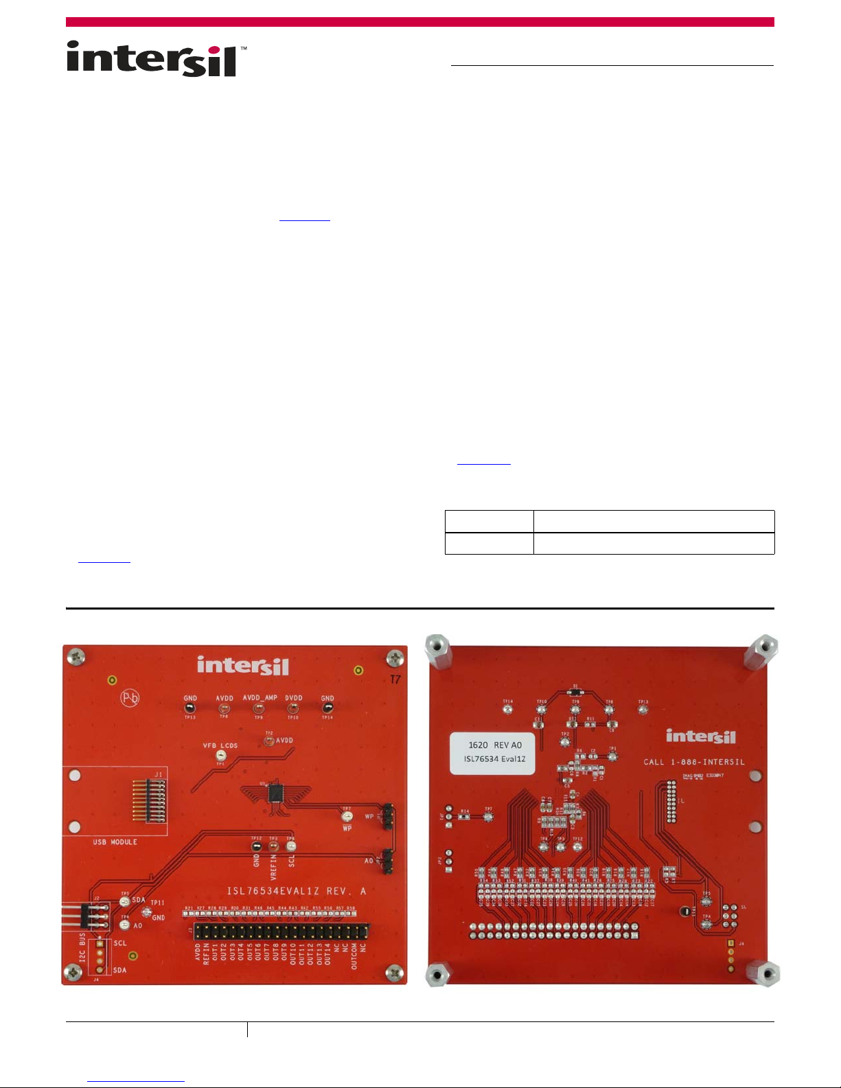
FIGURE 1. ISL76534EVAL1Z TOP VIEW FIGURE 2. ISL76534EVAL1Z BOTTOM VIEW
July 25, 2016
UG083.0
1
CAUTION: These devices are sensitive to electrostatic discharge; follow proper IC Handling Procedures.
1-888-INTERSIL or 1-888-468-3774
Intersil (and design) is a trademark owned by Intersil Corporation or one of its subsidiaries.
All other trademarks mentioned are the property of their respective owners.
| Copyright Intersil Americas LLC 2016. All Rights Reserved
Page 2
User Guide 083
SCL
SDA
A
VDD
D
VDD
I2C
INTERFACE
ANALOG
POWER
SUPPLY
DIGITAL
POWER
SUPPLY
REF
IN
RAM
14x10
CONTROL
BYTE
EEPROM
V
COM
DAC
10
GND
DAC15
GND
REF
IN
WP
WP: ACTIVE LOW
OUT1
OUT2
V
COM
AMPLIFIER
DAC1
10
10
DAC2
OUT3
10
DAC3
OUT4
OUT5
DAC4
10
10
DAC5
OUT6
10
DAC6
OUT7
OUT8
DAC7
10
10
DAC8
OUT9
10
DAC9
OUT10
OUT11
DAC10
10
10
DAC11
OUT12
10
DAC12
OUT13
OUT14
DAC13
10
10
DAC14
GND
OUTCOM
INN_COM
DAC/OUTx
BUFFER
A
VDD
_AMP
GND
A0
+
-
Submit Document Feedback
2
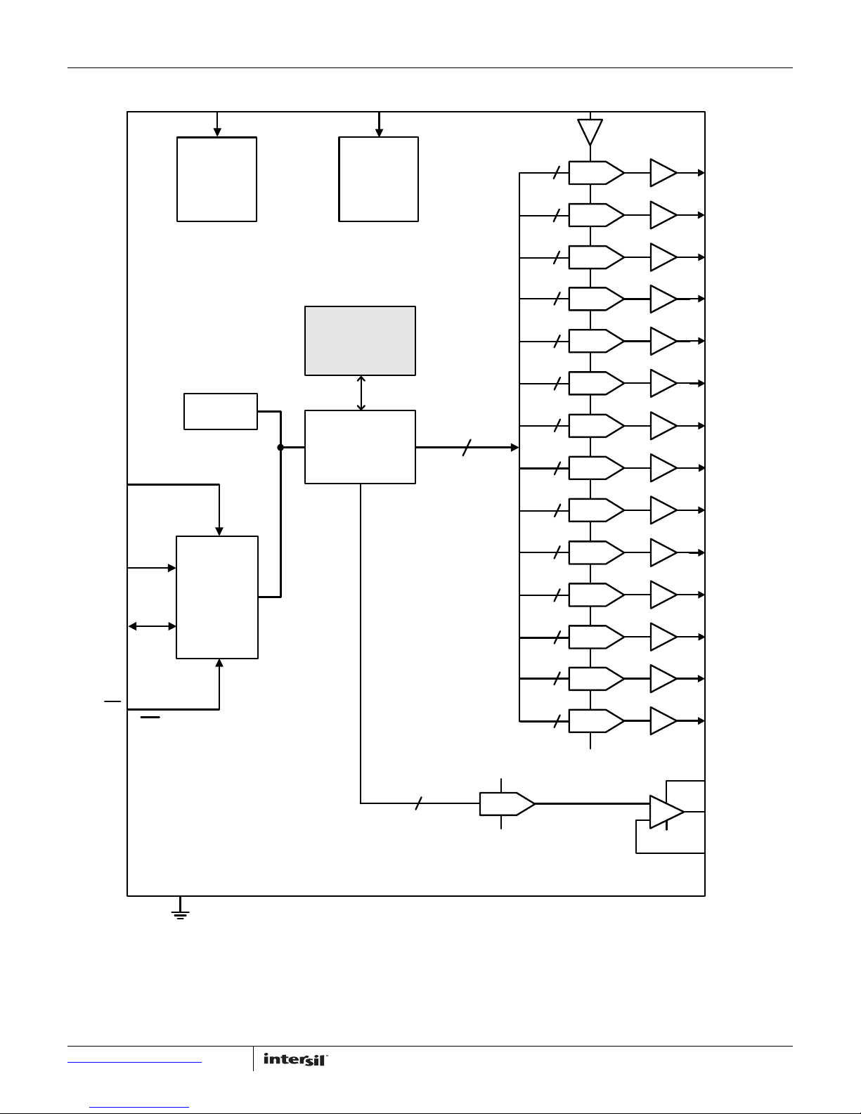
FIGURE 3. BLOCK DIAGRAM
UG083.0
July 25, 2016
Page 3
User Guide 083
USB FROM
PC/LAPTOP
PLUG IN USB
MODULE TO
POWER
SUPPLY 1
POWER
SUPPLY 2
DIGITAL
MULTIMETER (V)
OSCILLOSCOPE
TO TIME
TO VBAT
BOARD
What Is Inside
The evaluation kit contains:
• ISL76534EVAL1Z board
•The ISL76534
datasheet
• This ISL76534EVAL1Z user guide
• ISLUSBMINIZEVAL1Z (USB to I2C module)
What Is Needed
The following instruments will be needed to perform testing:
• Power supplies:
-PS1: DC 20V/5A, (between A
-PS2: DC 20V/5A, (between D
•Multimeters
• Oscilloscope
• Cables and wires
and A
VDD
and GND)
VDD
_AMP and GND)
VDD
Initial Set-Up
This user guide describes how to set up and use the
ISL76534EVAL1Z evaluation board along with the
ISLUSBMINIZEVAL1Z in a standalone configuration. It explains
how to install the software and how to use the Windows interface
to read and write to the ISL76534 data register and EEPROM.
Evaluation Software
The next section explains how to install the Graphical User
Interface (GUI) software, which is used to configure the ISL76534
data registers and EEPROM.
Notes
The GUI software was developed on a 64-bit Windows 8 platform.
Because the GUI software registers as a Human Interface Device
(HID) and uses standard HID calls, it should also work on other
XP or later Windows operating systems (32-bit and 64-bit),
including Windows 7.
This user guide contains screenshots of the GUI at the time this
user guide was written. Subsequent GUI versions may appear
differently.
Submit Document Feedback
3
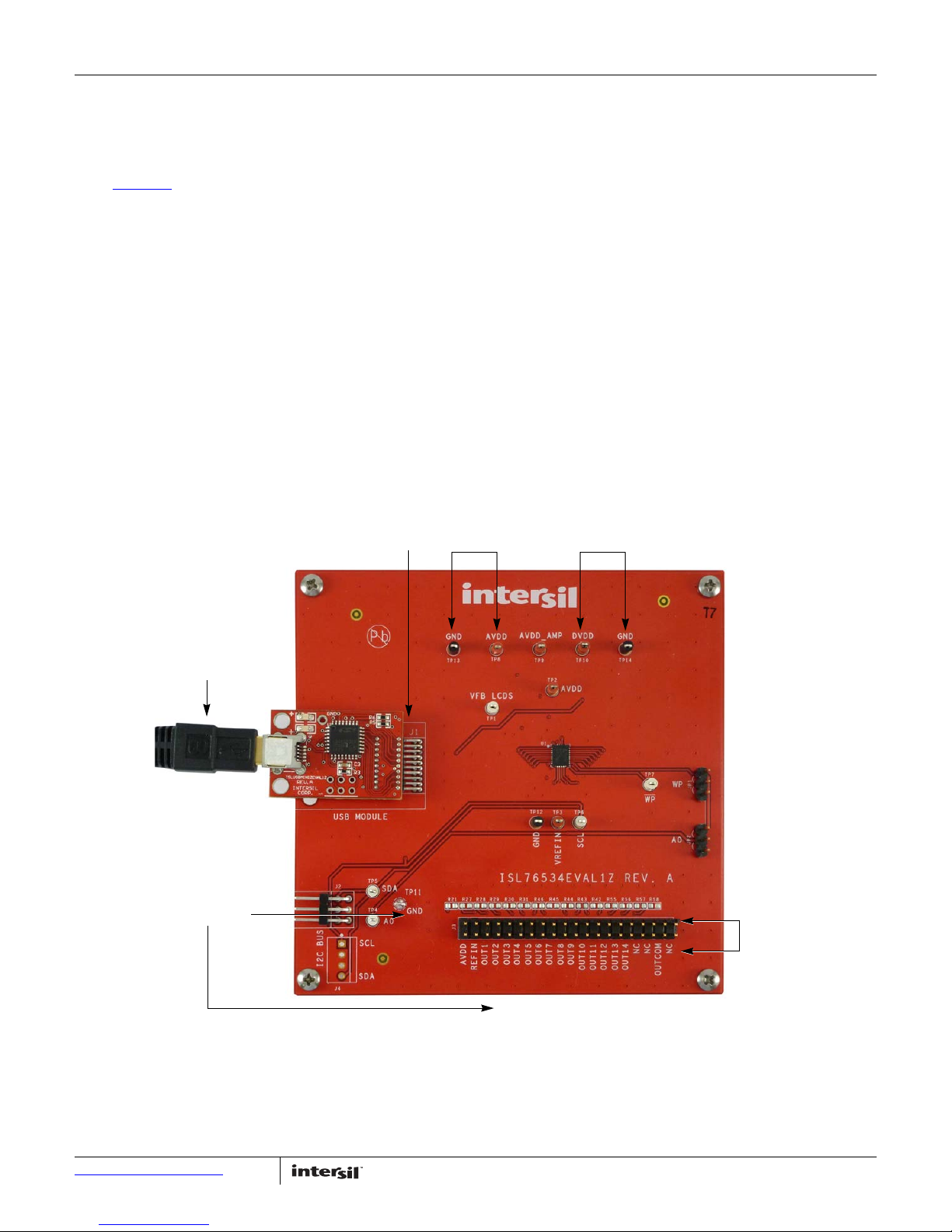
FIGURE 4. EXTERNAL CONNECTIONS AND JUMPERS
UG083.0
July 25, 2016
Page 4
User Guide 083
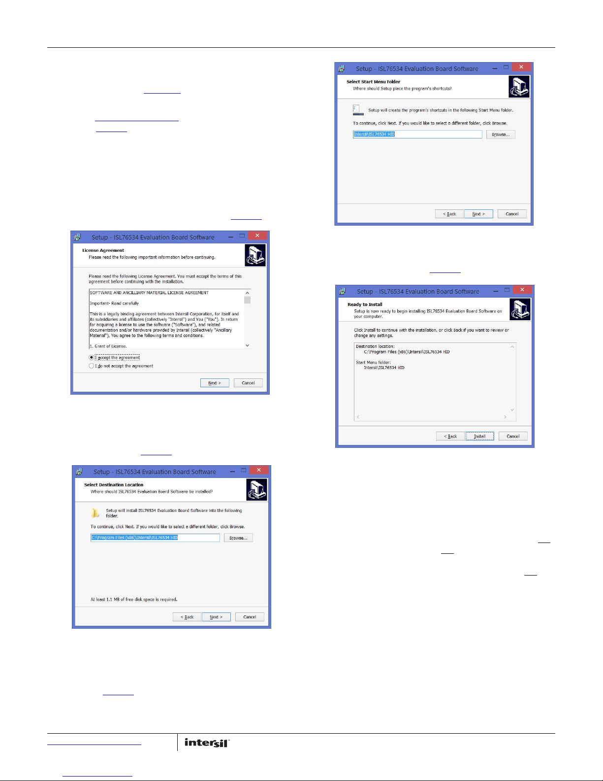
FIGURE 5. LICENSE AGREEMENT
FIGURE 6. SELECT DESTINATION LOCATION
FIGURE 7. SELECT START MENU FOLDER
FIGURE 8. BEGIN INSTALLATION
Software Installation Guide
The ISL76534EVAL1Z software can be installed from an installer
file downloaded from the ISL76534 product information page on
the Intersil web site.
Launch the “isl76534_installer.exe
instructions (Figure 5). The default installation adds an “Intersil”
directory to the “Start Menu\Programs” tree. That directory will
contain a shortcut to the ISL76534 executable, and an
uninstaller.
The default install option places the main program files in the
C:\Program Files\Intersil\ISL76534 directory; however, the
location can be customized, if desired.
Click Next to continue to the license agreement (Figure 5
” file and follow the
).
Click Next to create the Intersil folder in the Start menu. The
Ready to Install window opens (Figure 8
).
Read the license agreement, choose to accept (or not accept) the
license agreement, then click Next. The Select Destination
Location window opens (Figure 6
To use a directory different from the default location, click the
Browse button. Click Next to continue to the Select Start Menu
Folder screen (Figure 7
).
).
Click Install to copy all the necessary files to the PC. Installation
is now complete. Reboot the PC if requested.
Hardware Set-up Guide
Initial Board Jumper Positioning
JP1 - Is used to set the logic level of the Write Protection pin WP.
Shorting JP1-1 and -2 grounds the WP and prevents I2C data
write to the internal DAC registers. This is the default if the pin is
left floating. Shorting JP1-2 and -3 provides a high on the WP
thereby allows a data write to the internal DAC registers. Note the
pin has an internal pull down to GND.
2
JP2 - This pin determines the 7-bit I
JP1-1 and -2 grounds the A0 and sets it to low which equates to a
device address of 0x74. This is the default setting if the pin is left
floating. Shorting JP1-2 and -3 provides a high on the A0, which
sets the I
pin has an internal pull down to GND.
After the software is installed, the evaluation board is ready to be
interfaced through the PC.
2
C address to 0x75 (pulled up externally). Note that the
C device address. Shorting
and
Submit Document Feedback
4
UG083.0
July 25, 2016
Page 5
User Guide 083
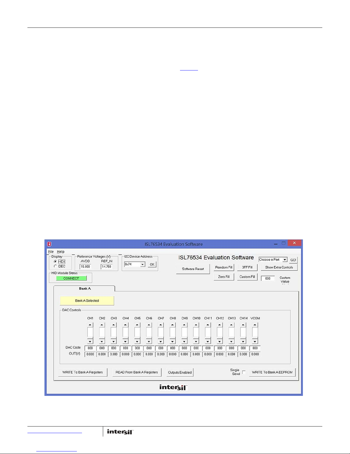
FIGURE 9. EVALUATION SOFTWARE WINDOW
1. Verify that the WP0 on JP1 is tied high if you wish to write to
the device register/EEPROM.
2. Using jumper JP2 tie A0 = LOW for an I2C address of 0x74 OR
A0 = HIGH for an I
2
C address of 0x75.
3. Connect the power supply ground(s) to the GND posts TP13
and TP14.
4. Apply 15V (range = 4.5V to 19V) to the A
VDD
and A
VDD
_AMP
analog supply posts TP8 and TP9.
5. Apply digital supply (2.25 to 3.6V) to the V
post TP10.
DD
6. Verify that the correct voltage is present across the power
supply pins and that the board is drawing reasonable current.
To ver ify at A
= 15V and D
VDD
VDD
= 3.3V, I
AVDD
is about
1.9mA (typical) and IDD is about 160μA (typical).
7. Connect the evaluation board to the PC with a USB cable.
USB Module Installation
When the ISLUSBMINIZEVAL1Z USB module is initially connected
to the PC, Windows may display the Found New Hardware pop-up
message.
This message means the USB module is registering itself as an
HID on your computer. The process should complete within a few
seconds.
On XP systems, a pop-up message may appear, displaying the
status of the USB module hardware.
If a Found New Hardware window appears asking for the location
of device drivers, please contact Intersil for a new USB module.
Using the Software GUI
Launch the software from the default location:
Start Menu\Programs\Intersil\ISL76534
After the program launches, you should see the screen shown in
Figure 9
10. REF
11. Set the appropriate I
12. Choose Zero Fill to write 0x00 to all registers.
13. Choose 3FF Fill to write 0x3FF to all the registers.
14. Choose Custom Fill to write a user defined value to all the
15. Probe the OUT
16. Probe the V
17. Turn off all supplies and disconnect the USB interface from
.
8. Set Display = HEX
9. A
= 15V (Actual voltage setting on the A
VDD
= 14.75V (REF
_IN
on the evaluation board).
A
VDD
is divided down to this value from
_IN
2
C address on the GUI and click OK.
VDD
supply).
registers after entering the value in the Custom Value input
box. The data sliders can also be used to vary individual
register value setting if needed.
to OUT
1
and read the programmed voltage
14
level based on the data written to the registers or EEPROM.
node and verify that it outputs the
COM
programmed voltage level based on the data written to the
registers or EEPROM.
the PC.
Submit Document Feedback
5
UG083.0
July 25, 2016
Page 6
User Guide 083
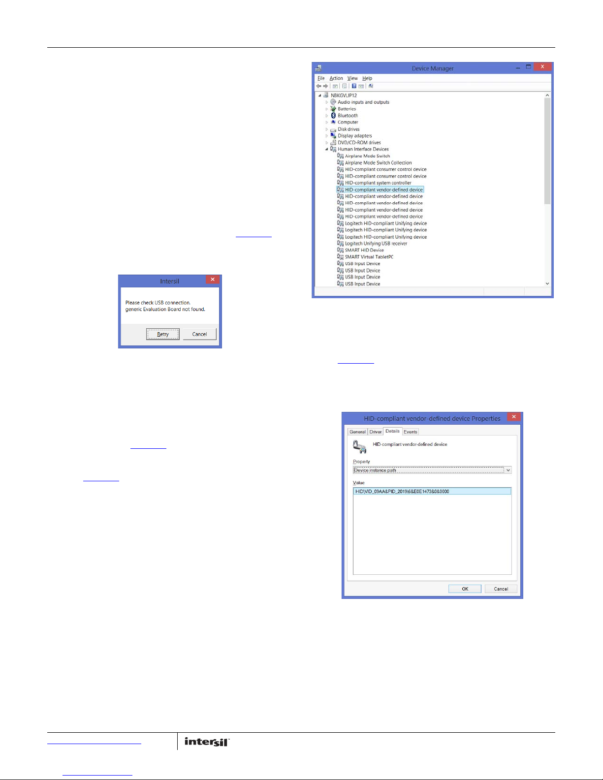
FIGURE 10. DEVICE NOT CONNECTED
FIGURE 11. DEVICE MANAGER WINDOW
FIGURE 12. VERIFY VID = 09AA&PID = 2019
Evaluation Software Troubleshooting
Verify that I2C signals can be detected on the SDA and SCL pins.
If they cannot, check the connection between the evaluation
board and the USB module. When trying to run the ISL76534
evaluation software, the occurrence of: “Run-time error number
'429': Active X component can't create object” means that your
computer does not have a sufficiently updated copy of
Microsoft.NET Framework. Microsoft.NET Framework can be
downloaded from the Microsoft web site at:
http://www.microsoft.com/net/download.aspx. Any version
from 2.0 and higher will work.
USB Driver Troubleshooting
The evaluation board software should be able to communicate
with the evaluation board as soon as it is launched. If there is a
communication problem, the dialog box shown in Figure 10
displayed. Click Retry to attempt to reconnect, or click Cancel to
exit the application.
is
After rebooting the PC, verify that the following files are in the
following locations:
• ISL76534.exe in C:\Program Files\Intersil\ISL76534
• isilhid.dll in C:\Program Files\Intersil\ISL76534
If the dialog shown in Figure 10
Control Panel. Double-click the System icon, select the Hardware
tab, and then click Device Manager. The Device Manager window
shown in Figure 11
Click Human Interface Devices to expand the folder. You should
see HID-compliant Device and an extra USB Human Interface
Device subcategory when the USB module is plugged in. This
indicates the driver is properly installed and is communicating
with the evaluation board.
opens.
persists, open the Windows
To verify that the new entries are actually the USB module,
right-click on HID-compliant Device and in the drop-down menu,
click Properties. The HID-compliant device Properties window
opens (Figure 12
should see a string, “HID\VID_09AA and PID_2019”
corresponding to the Vendor ID and Product ID of the USB
module. The Vendor ID = 0x09AA, and the Product ID = 0x2019.
). Click the Details tab. In the text window, you
Submit Document Feedback
6
UG083.0
July 25, 2016
Page 7

User Guide 083
If the Vendor ID and Product ID are not visible, or if there are any
error messages, try the following actions:
• Verify that the evaluation board has power and that the USB
cable is connecting the evaluation board and the PC.
• Disconnect and then reconnect the USB cable. You should hear
two tones from the PC speakers when the USB device is
enumerated.
• Cycle the power to the board.
• Close all instances of the ISL76534 application and restart the
software. Restart the PC if necessary.
• If none of this works, try installing the software on a different
PC to isolate the cause to the PC versus the evaluation board.
PCB Layout Recommendations
Good Printed Circuit Board (PCB) layout is necessary for optimum
performance. The following are recommendations to achieve
optimum high frequency performance from your PCB.
• To optimize thermal performance, solder the ISL76534’s
exposed thermal pad to GND. PCB vias should be placed below
the device’s exposed thermal pad and connected to GND to
transfer heat away from the device (see “General PowerPAD
Design Considerations” in the ISL76534
thermal pad is not connected to GND then it should be
electrically isolated.
datasheet). If the
• Maximize use of AC decoupled PCB layers. All signal I/O lines
should be routed over continuous ground planes (i.e., no split
planes or PCB gaps under these lines). Avoid vias in the signal
I/O lines.
• When testing, use good quality connectors and cables, match
cable types and keep cable lengths to a minimum.
• A minimum of two power supply decoupling capacitors are
recommended (typically 4.7µF and 0.1µF) per supply and
placed as close to the IC as possible. Avoid placing vias
between the capacitor and the device because vias add
unwanted inductance. Larger value capacitors can be placed
farther away (see “
For optimal thermal performance, use vias to distribute heat
away from the IC and to a system power plane. Fill the thermal
pad area with vias that are spaced 3x their radius (typically),
center-to-center, from each other. The via diameters should be
kept small, but they should be large enough to allow solder
wicking during reflow. To optimize heat transfer efficiency, do not
connect vias using “thermal relief” patterns. Vias should be
directly connected to the plane with plated through-holes.
Connect all vias to the correct voltage potential (power plane)
indicated in the datasheet. For the ISL76534, the thermal pad
potential is ground (GND).
PCB Layouts” starting on page 11).
Submit Document Feedback
7
UG083.0
July 25, 2016
Page 8
User Guide 083
8
UG083.0
July 25, 2016
Submit Document Feedback
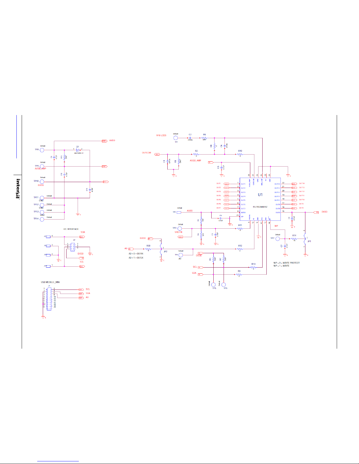
Schematic
FIGURE 13. SCHEMATIC
Page 9
User Guide 083
9
UG083.0
July 25, 2016
Submit Document Feedback
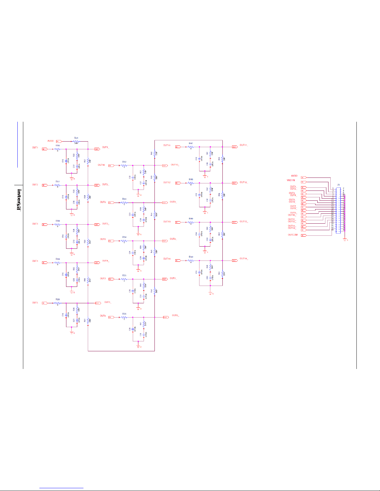
FIGURE 14. SCHEMATIC (Continued)
Schematic (Continued)
Page 10
User Guide 083
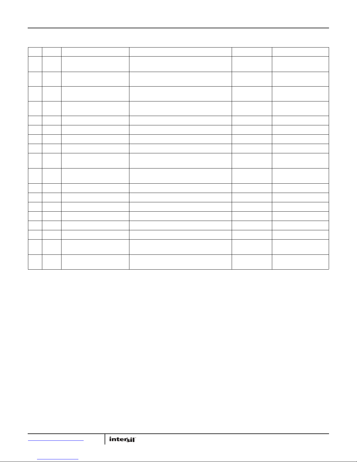
Bill of Materials
QTY UNITS REFERENCE DESIGNATOR DESCRIPTION MANUFACTURER PART NUMBER
1 ea. J4 (Do Not Populate), FOUR PIN FRICTION LOCK
5 ea. TP2, TP3, TP8-TP10 Miniature Red Test Point 0.100 Pad 0.040 Thole KEYSTONE 5000
4 ea. TP11-TP14 Miniature Black Test Point 0.100 Pad 0.040 Thole KEYSTONE 5001
5 ea. TP1, TP4-TP7 Miniature White Test Point 0.100 Pad 0.040 Thole KEYSTONE 5002
1 ea. D1 30V 200mA 200mW SCHOTTKY DIODE Diodes Inc BAT42W-7-F
3 ea. C9-C11 4.7µF, 35V, 10%, Ceramic Cap, X7R TDK CGA4J1X7R1V475K125AE
5 ea. C3-C5, C7, C8 0.1µF, 50V, 10% Multilayer Cap GENERIC H1045-00104-50V10
31 ea. C1, C2, C6, C12-C39 (Do Not Populate), Multilayer Cap GENERIC H1045-OPEN
34 ea. R1, R5-R7, R15, R21-R31,
R37-R46, R51-R58
22 ea. R2, R8-R13, R16-R20, R32-R36,
R47-R50, R59
1ea. R14 1kΩ,1%, 62.5mW, Thick Film Chip Resistor GENERIC H2511-01001-1/16W1
1 ea. U1 15Ch Programmable Gamma Buffer INTERSIL ISL76534ARXZ
2 ea. JP1, JP2 Three Pin Jumper GENERIC JUMPER-3-100
1 ea. J1 10/20 Pin Dual Row Header 0.5x0.5 HARWIN M50-3901042
1ea. R4 22kΩ, 1%, 62.5mW, Thick Film Chip Resistor Rohm MCR03ERTF2202
1ea. R3 330Ω, 1%, 62.5mW, Thick Film Chip Resistor Rohm MCR03ERTF3300
1 ea. J2 6 Pin Male Right Angle Header 2.54mmx2.54mm
1 ea. J3 40 Pin Header 2.54mmx2.54mm (0.100) SAMTEC TSW-40
ASSEMBLY
(Do Not Populate), Metal Film Chip Resistor GENERIC H2505-DNP-DNP-1
(Do Not Populate), Thick Film Chip Resistor GENERIC H2511-00R00-1/16W1
(0.100)
MOLEX 22-11-2042
SAMTEC TSW-103-08-T-D-RA
Submit Document Feedback
10
UG083.0
July 25, 2016
Page 11
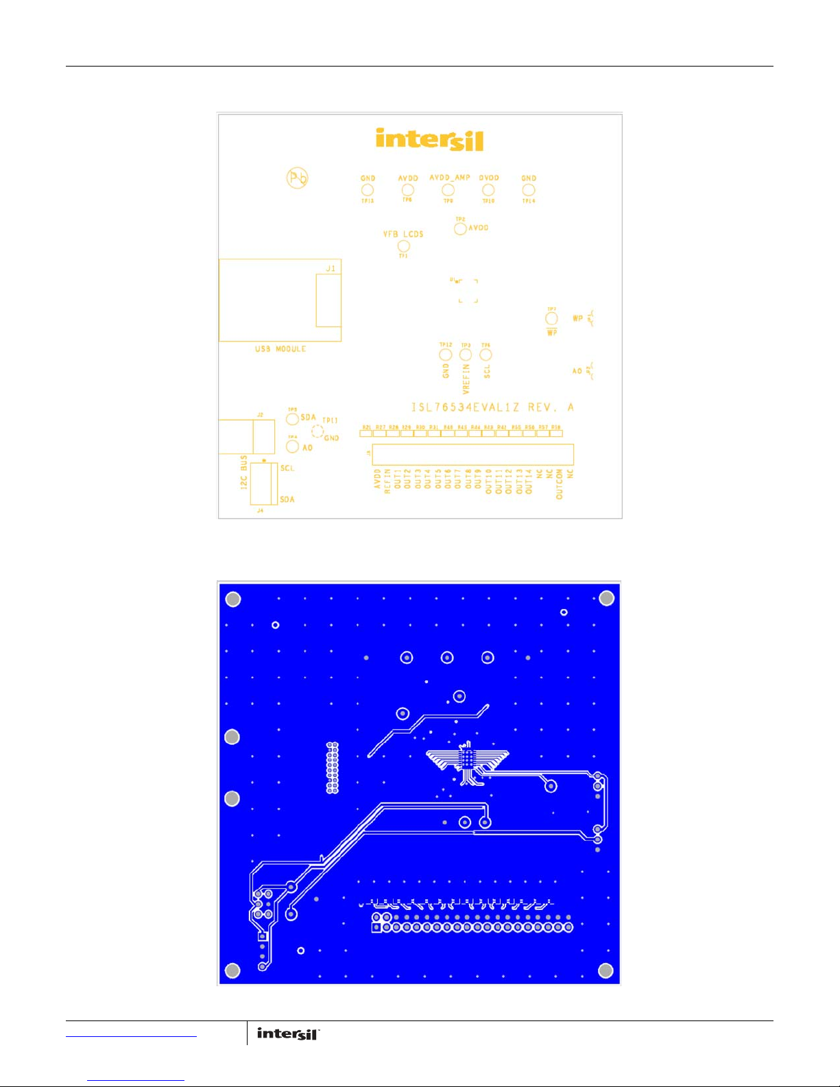
PCB Layouts
User Guide 083
FIGURE 15. SILK LAYER TOP
Submit Document Feedback
11
FIGURE 16. TOP LAYER COMPONENT SIDE
UG083.0
July 25, 2016
Page 12
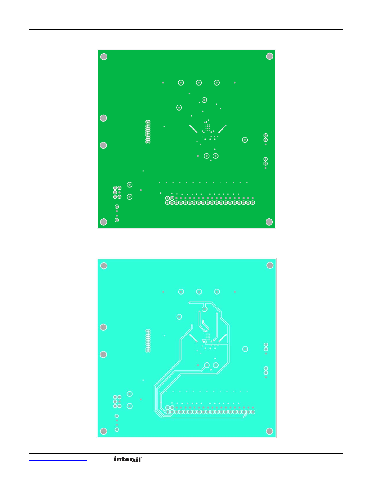
PCB Layouts (Continued)
User Guide 083
FIGURE 17. INTERNAL (LAYER 2)
Submit Document Feedback
12
FIGURE 18. INTERNAL (LAYER 3)
UG083.0
July 25, 2016
Page 13
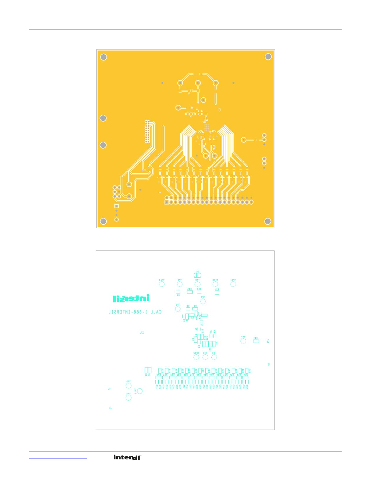
PCB Layouts (Continued)
User Guide 083
FIGURE 19. BOTTOM LAYER SOLDER SIDE
Submit Document Feedback
13
FIGURE 20. SILKSCREEN BOTTOM
UG083.0
July 25, 2016
Page 14
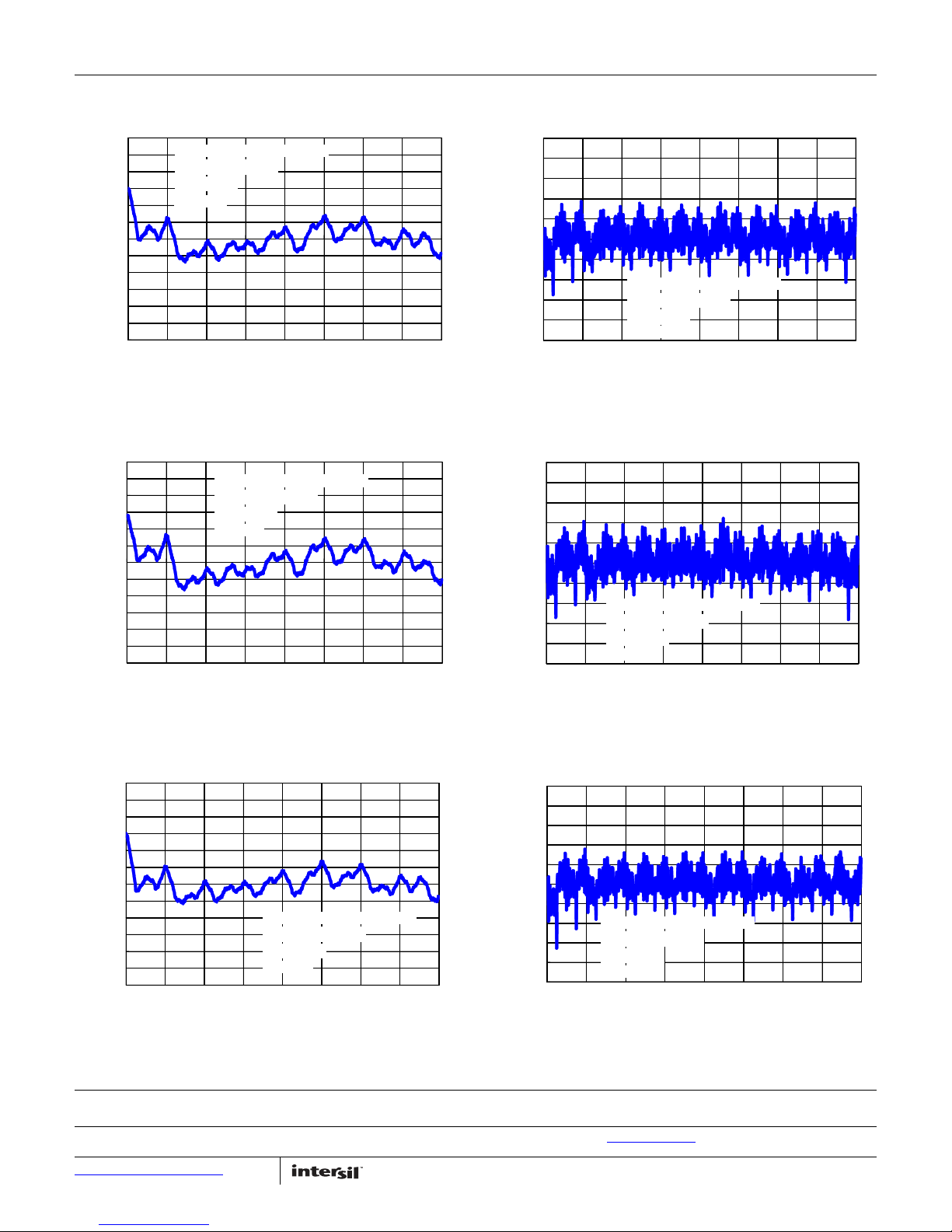
Typical Performance Curves
-1.2
-0.8
-0.4
0.0
0.4
0.8
1.2
0 128 256 384 512 640 768 896 1024
DAC CODE (DEC)
LINEARITY (LSB)
TYPICAL PRODUCTION UNIT
A
VDD
= REFIN = 15V
D
VDD
= 3.3V
NO LOAD
-0.10
-0.08
-0.06
-0.04
-0.02
0.00
0.02
0.04
0.06
0.08
0.10
0 128 256 384 512 640 768 896 1024
DAC CODE (DEC)
DNL (LSB)
TYPICAL PRODUCTION UNIT
A
VDD
= REFIN = 15V
D
VDD
= 3.3V
NO LOAD
-1.2
-0.8
-0.4
0.0
0.4
0.8
1.2
0 128 256 384 512 640 768 896 1024
DAC CODE (DEC)
TYPICAL PRODUCTION UNIT
A
VDD
= REFIN = 15V
D
VDD
= 3.3V
NO LOAD
LINEARITY (LSB)
-0.10
-0.08
-0.06
-0.04
-0.02
0.00
0.02
0.04
0.06
0.08
0.10
0 128 256 384 512 640 768 896 1024
DAC CODE (DEC)
DNL (LSB)
TYPICAL PRODUCTION UNIT
A
VDD
= REFIN = 15V
D
VDD
= 3.3V
NO LOAD
-1.2
-0.8
-0.4
0.0
0.4
0.8
1.2
0 128 256 384 512 640 768 896 1024
DAC CODE (DEC)
TYPICAL PRODUCTION UNIT
A
VDD
= REFIN = 15V
D
VDD
= 3.3V
NO LOAD
LINEARITY (LSB)
-0.10
-0.08
-0.06
-0.04
-0.02
0.00
0.02
0.04
0.06
0.08
0.10
0 128 256 384 512 640 768 896 1024
DAC CODE (DEC)
TYPICAL PRODUCTION UNIT
A
VDD
= REFIN = 15V
D
VDD
= 3.3V
NO LOAD
DNL (LSB)
User Guide 083
FIGURE 21. DAC1-DAC15 INL (REFIN=A
FIGURE 23. DAC1-DAC15 TYPICAL INL (REF
= 15V) AT +25°C
VDD
IN=AVDD
FIGURE 22. DAC1-DAC15 DNL (REF
IN=AVDD
= 15V) AT -40°C FIGURE 24. DAC1-DAC15 TYPICAL DNL (REFIN=A
= 15V) AT +25°C
= 15V) AT -40°C
VDD
FIGURE 25. DAC1-DAC15 INL (REF
IN=AVDD
Intersil Corporation reserves the right to make changes in circuit design, software and/or specifications at any time without notice. Accordingly, the reader is
cautioned to verify that the document is current before proceeding.
Submit Document Feedback
For information regarding Intersil Corporation and its products, see www.intersil.com
14
= 15V) AT +105°C FIGURE 26. DAC1-DAC15 DNL (REFIN=A
= 15V) AT +105°C
VDD
UG083.0
July 25, 2016
 Loading...