

Page 1
VEE
CO
C1
C2
C32
.
.
.
RELAY
RELAY
+
-
-34V
VDD
A0 A1 A2 A3 A4 EN
ISL72813SEH
ONE FOR EACH CHANNEL
EVALUATION BOARD
6
User Guide 096
ISL72813SEHEV1Z Evaluation Board User Guide
Description
The ISL72813SEHEV1Z evaluation board was designed to
provide a quick and easy method for evaluating the
ISL72813SEH
, 32-channel driver circuit IC. This device is a
unique IC. To use this evaluation board properly requires a
thorough knowledge of the operation of the IC. Refer to the
ISL72813SEH
datasheet for an understanding of the functions
and features of the device.
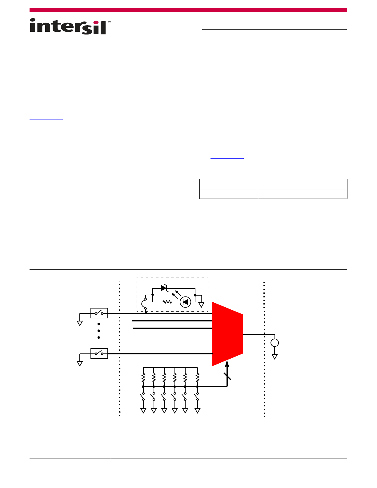
The Intersil ISL72813SEH device is a radiation hardened,
high-voltage, high-current 32-channel driver circuit with an
integrated decoder for driving and selecting between a bank of
relays in space applications. It is fabricated using Intersil’s
proprietary PR40 silicon-on-insulator process technology to
mitigate single-event effects. This device integrates 32 current
drivers that feature high-voltage, common-emitter and
open-collector outputs with a 42V breakdown voltage and
peak current rating of 600mA.
Specifications
The evaluation board has been configured and optimized for
the following conditions:
•V
= 5V
CC
= -34V
•V
EE
• Collector output (Cx) load to GND of ≥58Ω (≤600mA)
• Board temperature: +25°C
Key Features
• Toggle switches for easy control of logic pins
• LED circuitry for quick functional testing
• Convenient test points and connections for test equipment
• MCU interface connector for control of logic
• Banana jacks for power and ground connections
Related Literature
• For a full list of related documents, visit our website
- ISL72813SEH Datasheet
Ordering Information
PART NUMBER DESCRIPTION
ISL72813SEHEV1Z ISL72813SEH evaluation board
February 24, 2017
UG096.1
1
FIGURE 1. ISL72813SEHEV1Z BLOCK DIAGRAM
CAUTION: These devices are sensitive to electrostatic discharge; follow proper IC Handling Procedures.
1-888-INTERSIL or 1-888-468-3774
Intersil (and design) is a trademark owned by Intersil Corporation or one of its subsidiaries.
| Copyright Intersil Americas LLC 2016, 2017. All Rights Reserved
All other trademarks mentioned are the property of their respective owners.
Page 2

User Guide 096
Quick Start
1. Verify that jumpers J0 - J31 are installed on the board. This
connects the LED circuitry to each of the driver channels.
2. Put all of the toggle switches (SW0 A0, SW1 A1, SW2 A2,
SW3 A3, SW4 A4, and SW5 EN) in the down position. This
connects the A0 - A4, and EN logic pins of the IC to ground.
3. Apply 5VDC at the VCC banana jack.
4. Apply -30VDC at the VEE banana jack.
5. Move the SW5 EN toggle switch to the up position (EN = VCC)
to enable the current driver. The LED for the C0 channel will
light up indicating channel C0 is ON.
6. Move the SW0 A0 toggle switch to the up position. The LED for
the C1 channel will light up indicating that channel C1 is ON.
7. Adjust the toggle switches to cycle through the various 32
driver channels by changing the logic at the A0 - A4 pins per
the truth table on page 5 of the ISL72813SEH
datasheet.
Introduction
The ISL72813SEHEV1Z evaluation board is designed to provide a
quick and easy method for evaluating the ISL72813SEH
radiation hardened 32-channel current driver IC.
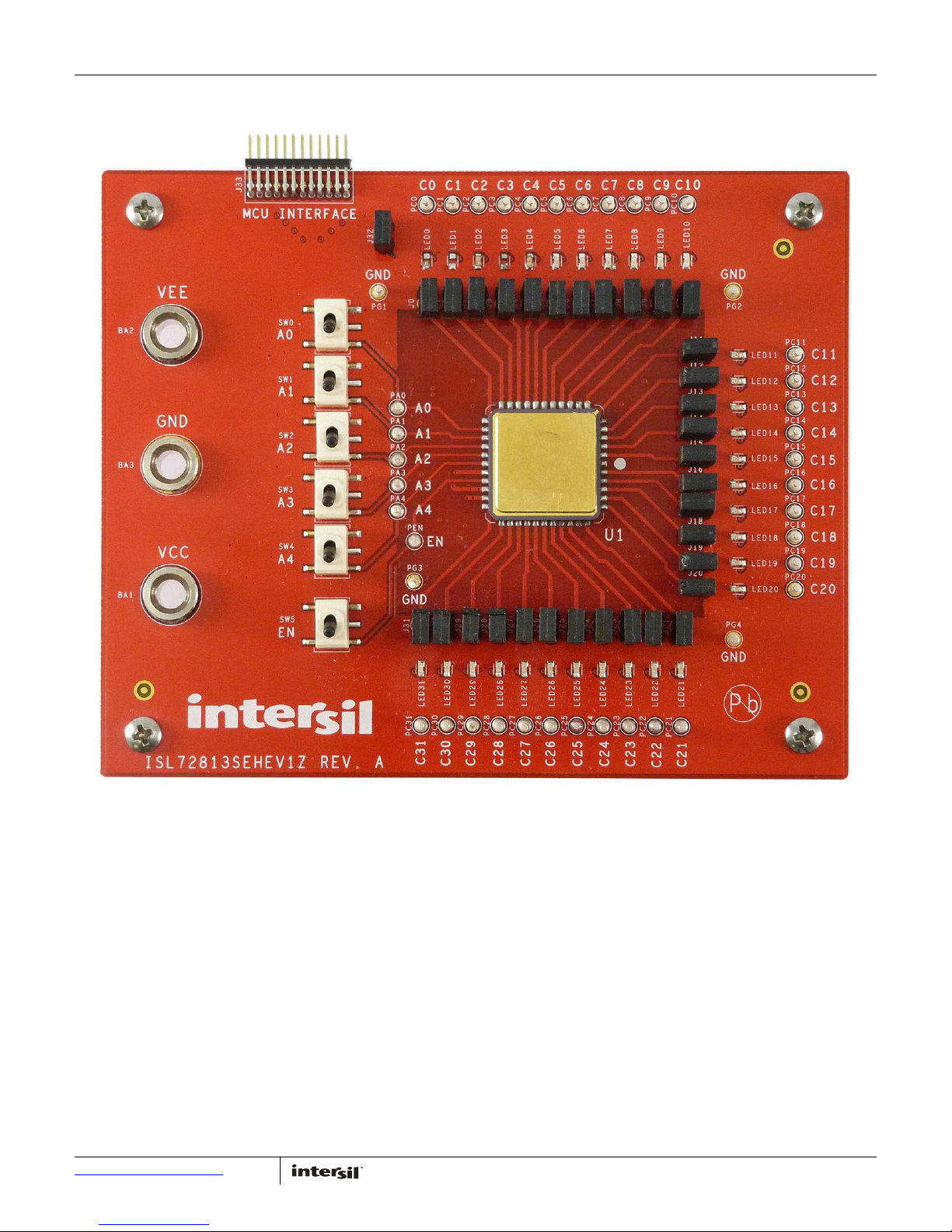
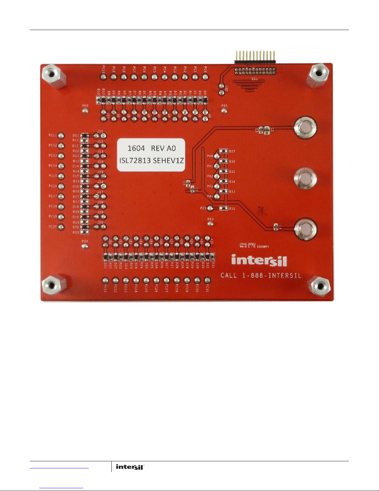
A picture of the evaluation board for ISL782813SEHEV1Z is
shown in Figure 3 on page 6
CLCC IC is soldered onto the evaluation board. It is located in the
center of the board and is designated as U1.
The Intersil ISL72813SEH device has 32 current driver channels.
It was specifically designed to drive the coils of a bank of relay
circuits. Only one channel is active at a time. A channel is
selected by the logic level applied at the A0 - A4 logic pins. It has
an enable pin (EN) that can deactivate all the channels when it is
driven LOW. A channel can drive a relay coil that requires up to
530mA of current. The part was designed to operate in the harsh
environment of space.
This user guide will guide the user through the process of
configuring and using the evaluation board to evaluate the
ISL72813SEH device.
. The ISL72813SEHL/PROTO 44 Ld
Functional Description
The ISL72813SEHEV1Z evaluation board provides a simple
platform to demonstrate the features and evaluate the
performance of the ISL72813SEH IC. It provides easy access to
the pins of the ISL72813SEH IC and convenient connectors/test
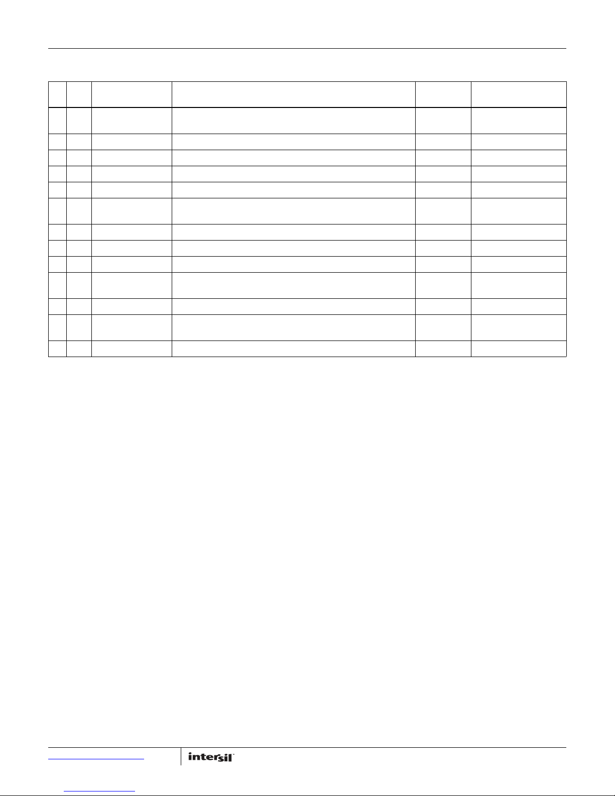
points for connecting test equipment. The schematic, bill of
materials, and top silkscreen for the board are available on
pages 9
Figures 13
ISL72813SEHEV1Z evaluation board and basic lab equipment.
The sections that follow will discuss using the evaluation board.
through 11.
through 15 show performance data taken using the
Basic Layout of Evaluation Board
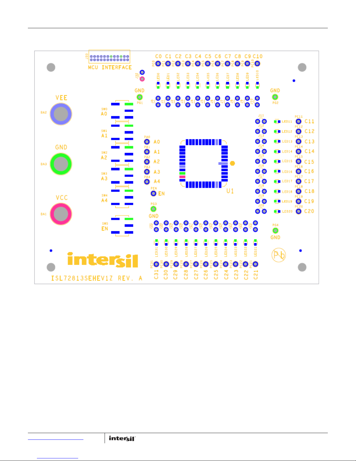
The basic layout of the evaluation board is as follows: Refer to
Figure 3 on page 6
board.
Located in the center of the board is the IS72813SEHL/PROTO
driver circuit IC (U1). The evaluation board has a Pin 1 dot, to
show how the IC should be oriented onto the evaluation board.
The IC Pin 1 indicator lead needs to be aligned with the
evaluation board Pin 1 dot indicator. The board comes with the IC
soldered onto the board.
Power for the IC is located at the left side of the board through
banana jacks labeled VEE, GND, and VCC. A negative DC voltage
source of -10V to -34V must be connected between VEE and GND
to power the common emitter of the current channels. A DC
voltage source of 3V to 5.5V must be connected between VCC
and GND to power the logic decoder and the level shifter of the
part.
Access to the 32 collector driver channels is through the C0 - C31
silver turret posts. The relay load or resistor simulating the relay
load would be connected at theses pins. Each pin in parallel to
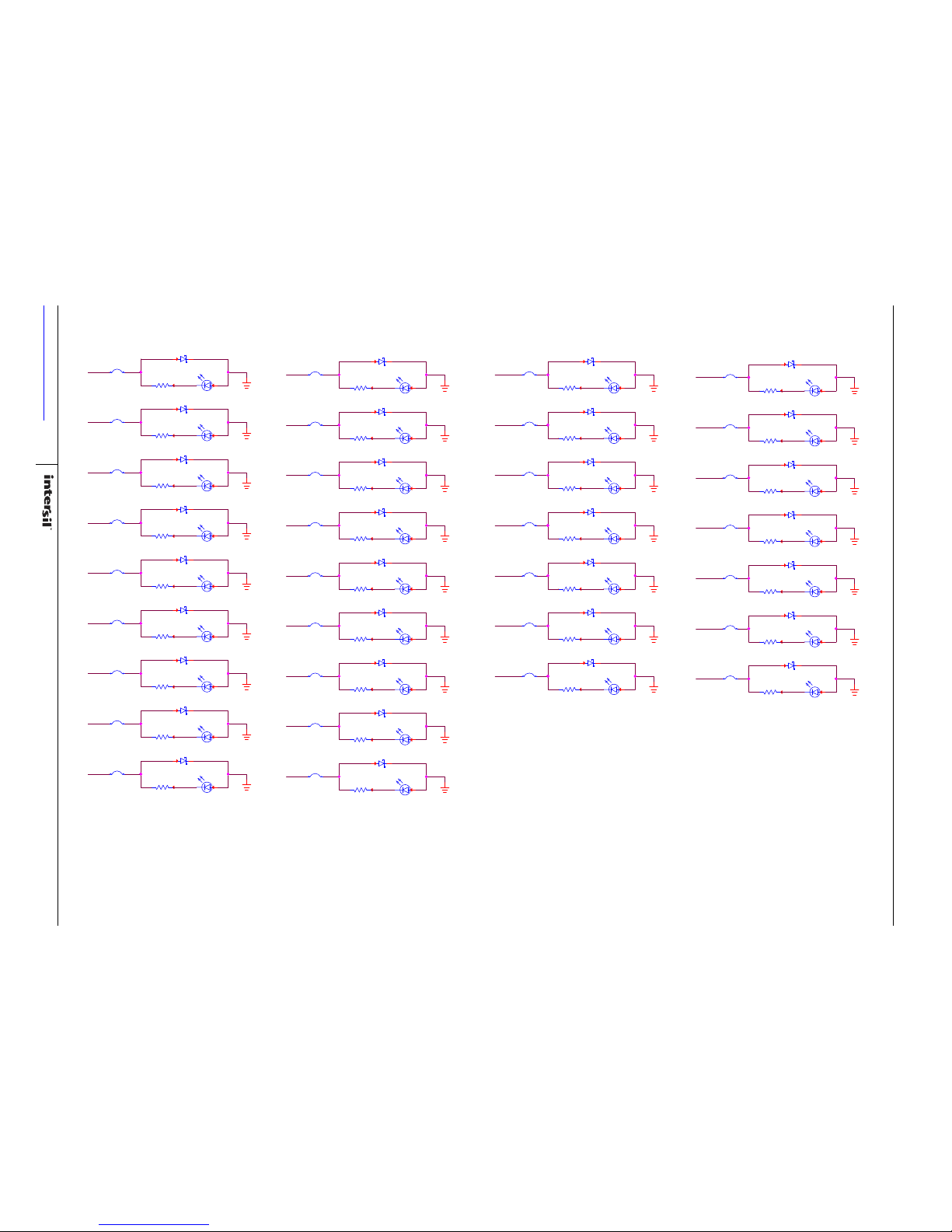
the turret post has an LED and resistor that can be connected
through a jumper to check the functionality of the device. With
jumpers J0 thru J31 installed the LED circuitry will be connected
to the C0 thru C31 open collectors of the part and when a
channel is active (turned ON), the LED will light up.
Control of the logic pins A0 - A4 and the EN pin is by the toggle
switches labeled SW0 A0, SW1 A1, SW2 A2, SW3 A3, SW4 A4,
and SW5 EN located at the middle left side of the evaluation
board. In addition to the switches, the logic can be controlled
through the 24 pin right angle header connector labeled “MCU
INTERFACE”. When using this connector, the toggle switches
should be switched into the up position. Finally, the logic can be
controlled by connecting the user’s logic drivers at the PA0 (A0),
PA1 (A1), PA2 (A2), PA3 (A3), PA4 (A4), and PEN (EN) turret pins.
When driving these pins, the toggle switches need to be in the up
position. These turret pins can also be used to monitor the
voltage levels at the logic pins with a voltmeter or oscilloscope.
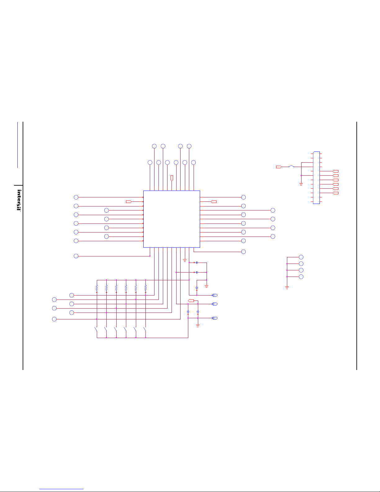
Refer to the board schematic (Figure 5 on page 8
reference designators of the jumpers, resistors, and connectors
associated with each I/O.
VCC Power Supply
The ISL72813SEH device requires a VCC DC voltage supply in the
range of 3.0V to 5.5V for proper operation. The VCC powers the
logic circuitry of the IC.
The VCC power supply is connected at banana jacks VCC and
GND. The power supply should be capable of delivering 100mA
of current.
VEE Power Supply
The ISL72813SEH device requires a negative VEE DC voltage
supply in the range of -5V to -34V. The VEE voltage is connected
to the common emitter of the 32 current drivers.
The power supply is connected at banana jacks VEE and GND.
The power supply should be capable of delivering 1A of current.
or the actual ISL72813SEHEV1Z evaluation
) for the
Submit Document Feedback
2
UG096.1
February 24, 2017
Page 3
User Guide 096
Logic Control
The ISL72813SEH IC has six logic control input pins; A0 - A4 (Pins
19 - 23) and EN (Pin 25).
The Logic 1 V
Logic 0 VIL level is from 0.8V to 0V. The VCC voltage can be 3.0V
to 5.5V.
The A0 - A4 digital input pins select between the 32 current
driver circuit channels per the truth table on page 5 of the
ISL72813SEH datasheet. The selected channel is activated when
the EN pin is HIGH (Logic 1).
The EN digital input enables and disables the current driver
channels. When EN = LOW (Logic 0) all channels are deactivated
(OFF). When EN = HIGH (Logic 1) then the channel selected by
the logic levels at A0 - A4 is activated (ON).
DESIGNATOR DESCRIPTION
SW0 A0 Toggle switch for logic input A0
SW1 A1 Toggle switch for logic input A1
SW2 A2 Toggle switch for logic input A2
SW3 A3 Toggle switch for logic input A3
SW4 A4 Toggle switch for logic input A4
SW5 EN Toggle switch for logic input EN
CO - C31 Open collector outputs load connections or test points
LED0 - LED31 LEDs for quick functional testing of the ISL72813SEH IC
R0 - R31 Load resistor for the LEDs
D0 - D31 Schottky diode across the LED circuitry to clamp positive transients during switching between channels
J0 - J31 Jumpers to connect LED circuitry to the open collector channel
level for the logic pins is from 2.0V to VCC. The
IH
TABLE 2. BOARD COMPONENT DEFINITIONS
U1 ISL72813SEHL/PROTO CLCC IC
VCC VCC power supply connection (5V
GND Ground connection
VEE Common emitter supply connection (-34V
DC
)
DC
)
Test Points
The board has various test points for ease of connecting probes
to make measurements. The test points available are described
in Table 1
.
TABLE 1. TEST POINTS
DESIGNATOR DESCRIPTION
PG1 - PG4 Ground test point
PA0 A0 logic input test point
PA1 A1 logic input test point
PA2 A2 logic input test point
PA3 A3 logic input test point
PA4 A4 logic input test point
PEN EN logic input test point
PC0 - PC31 Open collector output test points
Submit Document Feedback
3
UG096.1
February 24, 2017
Page 4
User Guide 096
C11
C12
C13
C14
C15
C16
C17
C18
C19
C20
C21
C22
C23
C24
C25
C26
C27
C28
C29
C30
C31
C10
C9
C8
C7
C6
C5
C4
C3
C2
C1
C0
ISL72813SEH
A0
A1
A2
A3
A4
EN
GND
VEE
GND
VCC
GND
GNDGND
SW0
A0
SW1
A1
SW2
A2
SW3
A3
SW4
A4
SW5
EN
ISL72813SEHEV1Z REV A
+5V
DC POWER SUPPLY
-
+
+34V
DC POWER SUPPLY
-
+
56Ω TO 4kΩ
H
L
H
L
H
L
H
L
H
L
H
L
+
-
A
IC0
+-V
VCE (SAT)
RESISTOR
DECADE
BOX
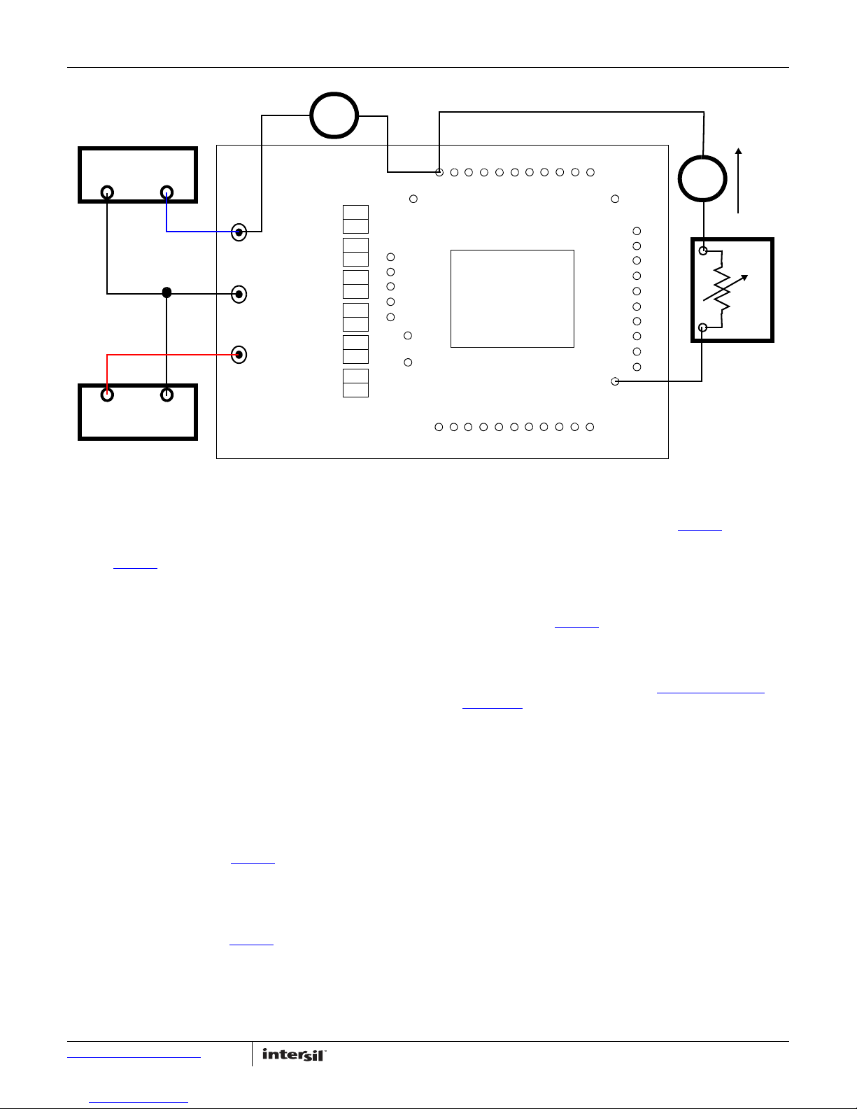
FIGURE 2. BASIC EVALUATION TEST SETUP BLOCK DIAGRAM (MEASURING VCE (SAT) vs ICx)
Using the Board to Measure
VCE (SAT) vs IVEE of Channel C0
Refer to Figure 2.
Lab Equipment
The equipment, external supplies, and signal sources needed to
operate the board:
1. DC power supply (3V to 5.5V).
2. DC power supply (-10V to -34V) capable of sinking 1A.
3. Resistor decade box or keysight B2902A precision
source/measurement unit or equivalent.
Initial Board Setup Procedure
1. Remove the J0 jumper to disconnect the LED circuitry from
the C0 channel.
2. Put the SW0 A0, SW1 A1, SW2 A2, SW3 A3, SW4 A4, and
SW5 EN toggle switches in the “L” down position. With the
SW5 EN in the “L” position all channels will be disabled (OFF).
3. Attach the 5VDC power supply to the banana jacks labeled
VCC and GND as shown in Figure 2
and negative terminal at GND. The supply should be capable
of delivering 3V to 5.5V and 100mA of current. Set the supply
voltage to 5V.
4. Attach the 34V
power supply to the banana jacks labeled
DC
VEE and GND as shown in Figure 2
and Positive terminal at GND. The supply should be capable of
-10V to -34V and sinking 1A of current. Set the supply voltage
to 34V.
Submit Document Feedback
4
. Positive terminal at VCC
. Negative terminal at VEE
5. Connect the resistor decade box and ammeter (A) to the C0
pin on the evaluation board as shown in Figure 2
. One end of
the decade box resistor should be connected to the C0 pin
through the ammeter to measure the IC0 current. The other
end of the resistor to the ground pin on the evaluation board.
Set the decade box resistance to 165Ω.
6. Connect a voltmeter (V) between the C0 pin and VEE banana
jack as shown in Figure 2
. The voltmeter will measure the
VCE (SAT) voltage.
VCE (SAT) Measurements for Channel C0
1. Configure the board as described in “Initial Board Setup
Procedure”.
2. Put the SW5 EN toggle switch in the “H” up position to enable
the IC. The IC0 current should read approximately 200mA and
the VCE (SAT) voltage should read around 0.89V.
3. Change the decade box resistance to 94Ω. The ICO current
should read approximately 349mA and the VCE (SAT) voltage
should read around 1.01V.
4. Change the decade box resistance to 65Ω. The ICO current
should read approximately 499mA and the VCE (SAT) voltage
should read around 1.13V.
5. Change the decade box resistance to 61Ω. The ICO current
should read approximately 532mA and the VCE (SAT) voltage
should read around 1.16V.
February 24, 2017
UG096.1
Page 5

User Guide 096
Measuring VCE (SAT) on Other Channels
1. Configure the board as described in “Initial Board Setup
Procedure” on page 4.
2. Ensure that SW5 EN toggle switch is in the “L” down position
to disable the IC.
3. Move the ammeter and decade box to the new Cx channel
that the user wants to test. Move the voltmeter to measure
the voltage from the new Cx channel to VEE. Remove the Jx
jumper from that channel. Configure the SW0 A0 - SW4 A4
toggle switches to the appropriate logic levels to select the
new Cx channel. Refer to the truth table on page 5 of the
ISL72813SEH
For example, if the user wants to perform the measurement
on the C26 channel, connect the ammeter/decade box at the
C26 pin on the evaluation board. Connect the voltmeter
across the C26 pin and VEE. Remove jumper J26 to
disconnect its LED circuitry. Set the toggle switches
SW0 A0 = “L”, SW1 A1 = “H”, SW2 A2 = “L”, SW3 A3 = “H”,
and SW4 A4 = “H”.
4. Repeat steps 2 - 5 in “
C0” on page 4 for the new Cx channel.
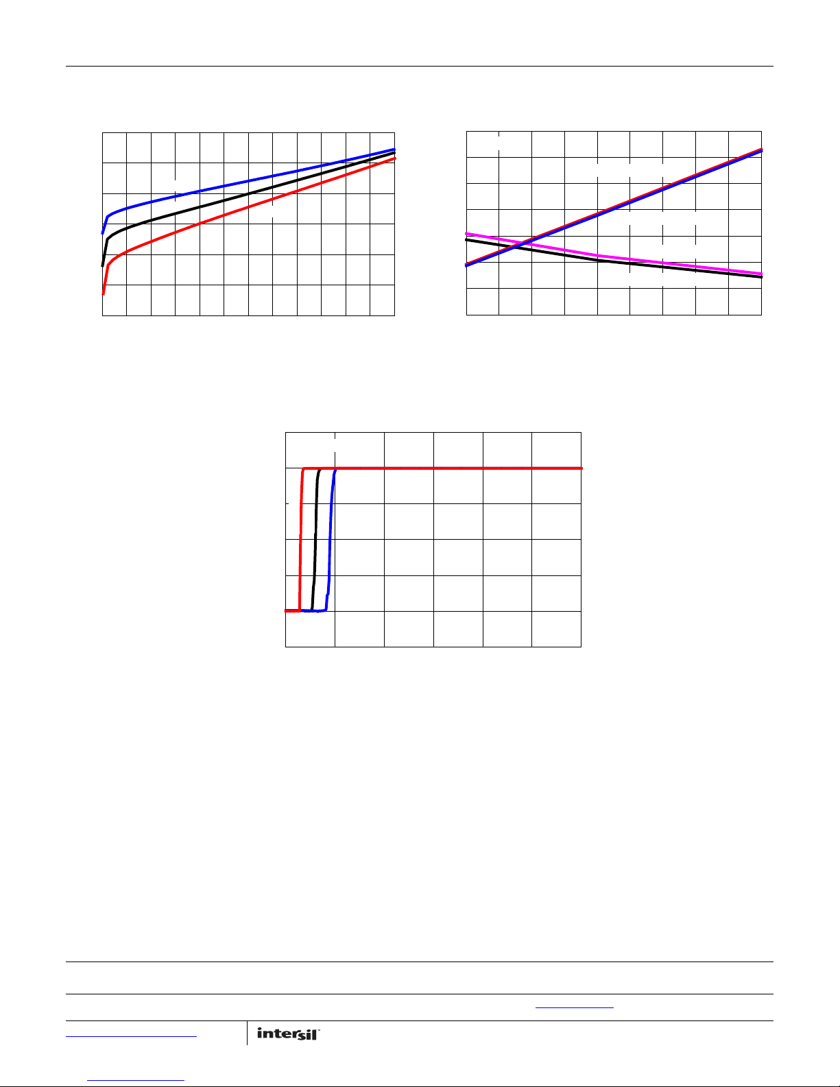
5. Note: The performance curves shown in Figure 13 on page 17
was taken using the evaluation board and a Keysight B2902A
precision source/measurement unit.
Test conditions:
a. The B2902A unit was set to measure and graph VCE
b. VCC = 5V, VEE = -34V, EN = VCC, A0 - A4 = Set to have
c. Channels CH0, CH8, CH16, CH24, and CH31 were
datasheet.
VCE (SAT) Measurements for Channel
(SAT) vs ICX as the user sweeps the ICX in 10mA
increments from 0mA to 600mA.
the Cx channel ON.
measured. The plots in Figure 13 are the average of
these channels.
Submit Document Feedback
5
UG096.1
February 24, 2017
Page 6
User Guide 096
ISL72813SEHEV1Z Evaluation Board
FIGURE 3. ISL72813SEHEV1Z EVALUATION BOARD (TOP VIEW)
Submit Document Feedback
6
UG096.1
February 24, 2017
Page 7
User Guide 096
ISL72813SEHEV1Z Evaluation Board (Continued)
FIGURE 4. ISL72813SEHEV1Z EVALUATION BOARD (BOTTOM VIEW)
Submit Document Feedback
7
UG096.1
February 24, 2017
Page 8
User Guide 096
8
UG096.1
February 24, 2017
Submit Document Feedback
ISL72813SEHEV1Z Circuit Schematic
FIGURE 5. SCHEMATIC PAGE 1
RELEASED BY:
DRAWN BY:
HRDWR ID
DATE:
DATE:
DATE:
TESTER
MASK#
DENGINEER:
TITLE:
UPDATED BY:
12/09/2015
ISL72813SEH
KIRAN BERNARD
32 CHANNEL CURRENT DRIVER
ENGINEERING SCHEMATIC
TIM KLEMANN
+5V
GND
GND
-30V
5
MCU INTERFACE CONNECTOR
E
E
E
E
E
IN
IN
OUT
IN
IN
IN
IN
IN
IN
IN
IN
PC3
PC24
PC19
PEN
PC2
J32
PC15
PC5
PC22
SW1
PA3
BA3
PC4
PG4
A4
VEEENGND
VCC
C31
C11
C12
C14
C15
VEE
C16
C17
C18
C20
C19
C21
VEE
C22
C23
C24
C25
C26
C27
C28
C29
C30
C2
C1
C3
C4
C5
C10
C8
C7
C6
A3A2A1A0C0
VEE
C9
C13
ISL72813SEHVL
U1
12345
6
7
8
9
10
11
12
13
14
15
16
17
1819202122232425262728
29
30
31
32
33
34
35
36
37
38
39
4041424344
PC7
PC21
R36
10K
PC20
PA1
BA2
PC6
PG3
PC9
PC29
SW0
1UF
C4
PA4
BA1
PC8
PG2
PC16
PC10
PC27
R37
10K
0.1UF
C3
PA2
PC31
SW3
PG1
PC17
SW5
PC25
PC11
C2
0.1UF
PA0
PC30
R34
10K
10K
R32
PC23
PC12
PC0
PC28
SW2
17
1
3
11
13
15
19
21
23
9
7
526
4
8
12
10
16
14
18
22
24
20
J33
PC18
SW4
PC13
0.1UF
C5
PC1
PC26
R35
10K
C1
1UF
10K
R33
PC14
A0
A0
A1
A1
A2
A2
A3
A3
A4
A4
C0
C1
C10
C11
C12
C13
C14
C15
C16
C17
C18
C19C2C20
C21
C22
C23
C24
C25
C26
C27
C28
C29
C3
C30
C31
C4
C5
C6
C7
C8
C9
EN
EN
UNNAMED_1_CONN24_I692_IN7
VCC
VCC
VEE
VEE
VEE
VEE
Page 9
User Guide 096
9
UG096.1
February 24, 2017
Submit Document Feedback
FIGURE 6. SCHEMATIC PAGE 2
ISL72813SEHEV1Z Circuit Schematic (Continued)
RELEASED BY:
DRAWN BY:
DATE:
DATE:
DATE:
TESTER
DATE:ENGINEER:
TITLE:
UPDATED BY:
12/09/2015
ISL72813SEH
TIM KLEMANN KIRAN BERNARD
ENGINEERING SCHEMATIC
32 CHANNEL CURRENT DRIVER
E
E
E
E
E
E
E
E
E
E
E
E
E
E
E
E
E
E
E
E
E
E
E
E
E
E
E
E
E
E
E
E
30.1K
R4
D16
LED20
LED5
30.1K
R31
J15
R23
30.1K
LED28
D4
LED16
J24
D29
J3
R15
30.1K
D21
30.1K
R3
D15
LED19
LED4
30.1K
R30
J14
30.1K
R22
LED27
D3
LED15
J31
J23
D28
J2
30.1K
R14
D20
R2
30.1K
D14
LED18
LED3
30.1K
R29
J13
30.1K
R21
LED26
D19
D2
LED14
J30
J22
D27
J1
30.1K
R13
30.1K
R1
D13
LED2
30.1K
R28
J12
30.1K
R20
LED25
J0
30.1K
R12
D18
D1
LED13
J29
J21
D26
R0
30.1K
D12
LED1
30.1K
R27
J8
J11
30.1K
R19
30.1K
R8
R11
30.1K
LED24
D0
LED12
J28
J20
D25
D8
D11
LED0
30.1K
R26
J7
J10
30.1K
R18
30.1K
R7
30.1K
R10
LED23
LED8
LED11
J27
J19
LED31
D7
D10
30.1K
R25
J6
J9
D24
30.1K
R6
30.1K
R9
LED22
LED7
LED10
J26
J17
J18
LED30
D6
D9
D31
J5
30.1K
R17
D23
R5
30.1K
D17
LED21
LED6
LED9
J25
J16
R24
30.1K
LED29
D5
LED17
D30
J4
30.1K
R16
D22
C0
C1
C10
C11
C12
C13
C14
C15
C16
C17
C18
C19
C2 C20
C21
C22
C23
C24
C25
C26
C27
C28
C29
C3
C30
C31
C4
C5
C6
C7
C8
C9
UNNAMED_2_JUMPER2_I195_IN2
UNNAMED_2_JUMPER2_I196_IN2
UNNAMED_2_JUMPER2_I197_IN2
UNNAMED_2_JUMPER2_I198_IN2
UNNAMED_2_JUMPER2_I199_IN2
UNNAMED_2_JUMPER2_I200_IN2
UNNAMED_2_JUMPER2_I201_IN2
UNNAMED_2_JUMPER2_I202_IN2
UNNAMED_2_JUMPER2_I203_IN2
UNNAMED_2_JUMPER2_I204_IN2
UNNAMED_2_JUMPER2_I205_IN2
UNNAMED_2_JUMPER2_I206_IN2
UNNAMED_2_JUMPER2_I207_IN2
UNNAMED_2_JUMPER2_I208_IN2
UNNAMED_2_JUMPER2_I209_IN2
UNNAMED_2_JUMPER2_I210_IN2
UNNAMED_2_JUMPER2_I211_IN2
UNNAMED_2_JUMPER2_I212_IN2
UNNAMED_2_JUMPER2_I213_IN2
UNNAMED_2_JUMPER2_I214_IN2
UNNAMED_2_JUMPER2_I215_IN2
UNNAMED_2_JUMPER2_I216_IN2
UNNAMED_2_JUMPER2_I217_IN2
UNNAMED_2_JUMPER2_I218_IN2
UNNAMED_2_JUMPER2_I219_IN2
UNNAMED_2_JUMPER2_I222_IN2
UNNAMED_2_JUMPER2_I223_IN2
UNNAMED_2_JUMPER2_I224_IN2
UNNAMED_2_JUMPER2_I225_IN2
UNNAMED_2_JUMPER2_I226_IN2
UNNAMED_2_JUMPER2_I227_IN2
UNNAMED_2_JUMPER2_I228_IN2
UNNAMED_2_SMLED_I133_B
UNNAMED_2_SMLED_I137_B
UNNAMED_2_SMLED_I140_B
UNNAMED_2_SMLED_I144_B
UNNAMED_2_SMLED_I148_B
UNNAMED_2_SMLED_I155_B
UNNAMED_2_SMLED_I158_B
UNNAMED_2_SMLED_I168_B
UNNAMED_2_SMLED_I172_B
UNNAMED_2_SMLED_I175_B
UNNAMED_2_SMLED_I179_B
UNNAMED_2_SMLED_I183_B
UNNAMED_2_SMLED_I190_B
UNNAMED_2_SMLED_I193_B
UNNAMED_2_SMLED_I29_B
UNNAMED_2_SMLED_I33_B
UNNAMED_2_SMLED_I38_B
UNNAMED_2_SMLED_I45_B
UNNAMED_2_SMLED_I50_B
UNNAMED_2_SMLED_I55_B
UNNAMED_2_SMLED_I60_B
UNNAMED_2_SMLED_I65_B
UNNAMED_2_SMLED_I70_B
UNNAMED_2_SMLED_I78_B
UNNAMED_2_SMLED_I81_B
UNNAMED_2_SMLED_I82_B
UNNAMED_2_SMLED_I85_B
UNNAMED_2_SMLED_I86_B
UNNAMED_2_SMLED_I89_B
UNNAMED_2_SMLED_I90_B
UNNAMED_2_SMLED_I93_B
UNNAMED_2_SMLED_I94_B
Page 10
User Guide 096
ISL72813SEHEV1Z Bill of Materials
REFERENCE
QTY UNITS
42 ea. PA0 - PA4, PC0-PC31,
1 ea. C4 CAP, Multilayer, 0603, 1µF, 10V, 10%, CAP_0603 MURATA GRM188R71A105KA61D
1 ea. C1 CAP, Ceramic, 0803, 1µF, 50V, 10%, CAP_0805 MURATA GRM21BR71H105KA12L
3 ea. C2, C3, C5 CAP, Multilayer, 0603, 0.1µF, 50V, 10%, CAP_0603 GENERIC H1045-00104-50V10
3 ea. BA1 - BA3 CONN; CON_BAN_575, Solder Mount Banana Plug KEYSTONE 575-4
6 ea. SW0 - SW5 SPST - GT13MSCKE - C&K - SPST OFF-ON SM (2 Switch Positions), Ultra
6 ea. R32 - R37 Thick Film Chip Resistor, 10kΩ, 1/10W, 1%, 0603, RES_0603 GENERIC H2511-01002-1/10W1
32 ea. R0 - R31 Thick Film Chip Resistor, 30.1kΩ, 1/16W, 1%, 0603, RES_0603 GENERIC H2511-03012-1/16W1
33 ea. J0 - J32 Two Pin Jumper, Thole, Jumper-1 GENERIC JUMPER2-100
32 ea. LED0 - LED31 SMD, LED_LX_L29K_0603, SMT 0603, GREEN, 1.7V, 2mA, 570nm,
32 ea. D0 - D31 Schottky Barrier Rectifier Diode, SMD2, SOD23, 0.5A DIODES B0540WS
1 ea. J33 PTH2X12A, CON_HDR_3X12_50_RA, Male, 24 PIN (2 ROWS X 12 POS
1 ea. U1 32-Channel Driver Circuit with Integrated Decoder INTERSIL ISL72813SEHL/PROTO
DESIGNATOR DESCRIPTION MFR
Silver Solder Terminal Turret, 0.08 Pad, 0.040 Thole MILL-MAX 2108-2-00-44-00-07-0
PEN, PG1-PG4
C&K GT12MSCBETR
Miniature Toggle Switch
OSRAM LG L29K-G2J1-24-Z-T
3.9MCD
HARWIN M50-3901242
at 0.05 IN), Right Angle Header Connector
MANUFACTURER
PART NUMBER
Submit Document Feedback
10
UG096.1
February 24, 2017
Page 11
Board Layout
User Guide 096
Submit Document Feedback
11
FIGURE 7. SILKSCREEN TOP
UG096.1
February 24, 2017
Page 12
Board Layout (Continued)
User Guide 096
Submit Document Feedback
12
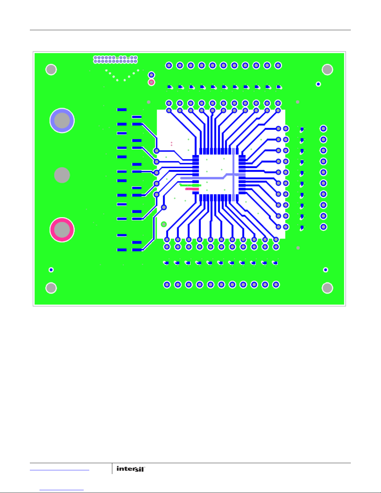
FIGURE 8. TOP LAYER COMPONENT SIDE
UG096.1
February 24, 2017
Page 13
Board Layout (Continued)
User Guide 096
Submit Document Feedback
13
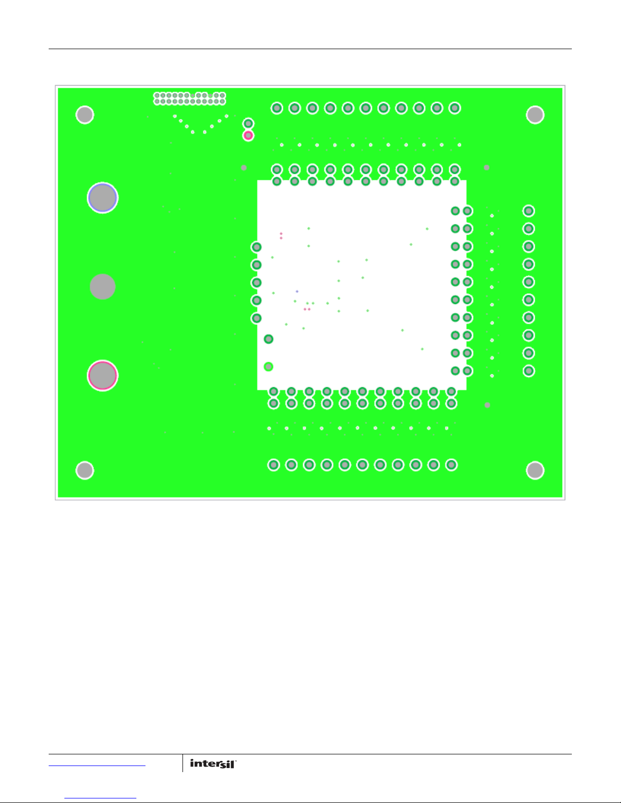
FIGURE 9. LAYER 2
UG096.1
February 24, 2017
Page 14
Board Layout (Continued)
User Guide 096
Submit Document Feedback
14
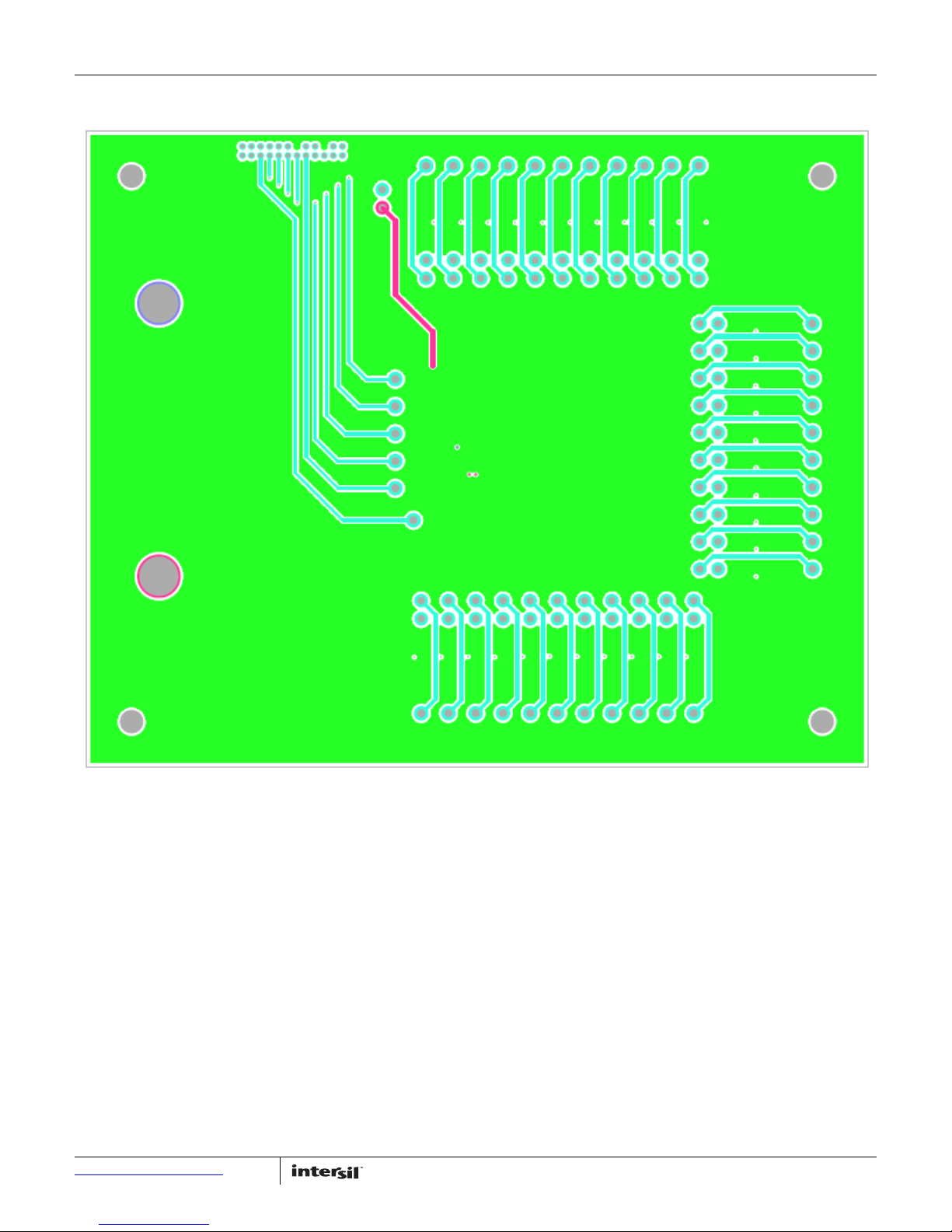
FIGURE 10. LAYER 3
UG096.1
February 24, 2017
Page 15
Board Layout (Continued)
User Guide 096
Submit Document Feedback
15
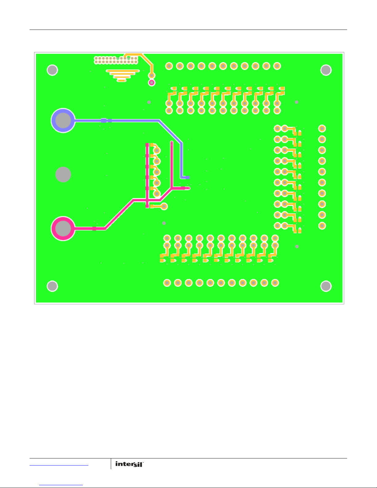
FIGURE 11. BOTTOM LAYER SOLDER SIDE
UG096.1
February 24, 2017
Page 16
Board Layout (Continued)
User Guide 096
Submit Document Feedback
16
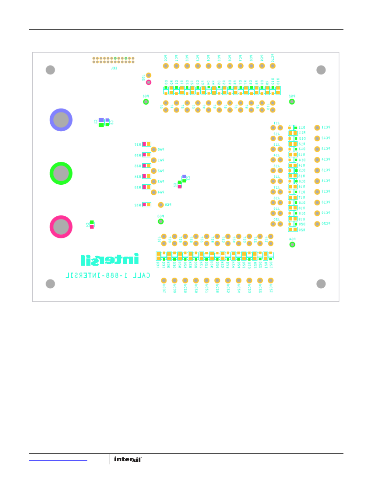
FIGURE 12. SILKSCREEN BOTTOM
UG096.1
February 24, 2017
Page 17
User Guide 096
0.2
0.4
0.6
0.8
1.0
1.2
1.4
0 50 100 150 200 250 300 350 400 450 500 550 600
VCE (SAT) (V)
IVEE or ICX (mA)
+25°C
-55°C
+125°C
0
1
2
3
4
5
6
7
-55 -35 -15 5 25 45 65 85 105 125
TIME (µs)
TEMPERATURE (°C)
t
ENABLE
(VCC = 3V)
t
ENABLE
(VCC = 5.5V)
t
DISABLE
(VCC = 5.5V)
t
DISABLE
(VCC = 3V)
RL = 64Ω
-25
-20
-15
-10
-5
0
5
-65 -55 -45 -35 -25 -15 -5
IEE (mA)
VEE (V)
+25°C
-55°C
+125°C
C0 - C31 = EN = 0V
Typical Performance Curves Unless noted: V
t
= tf ≤6ns, TA = +25°C
r
FIGURE 13. VCE (SAT) vs ICX vs TEMPERATURE FIGURE 14. t
= 3.3V, D = 125kHz, Square Wave, 0 to VCC, 50% Duty Cycle,
CC
ENABLE/tDISABLE
vs VCC vs TEMPERATURE
Intersil Corporation reserves the right to make changes in circuit design, software and/or specifications at any time without notice. Accordingly, the reader is
cautioned to verify that the document is current before proceeding.
Submit Document Feedback
For information regarding Intersil Corporation and its products, see www.intersil.com
17
FIGURE 15. IEE vs VEE vs TEMPERATURE
UG096.1
February 24, 2017
 Loading...