

Page 1
DATASHEET
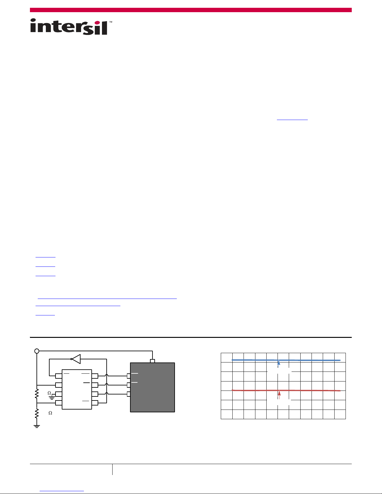
FIGURE 1. TYPICAL APPLICATION
1
2
3
4
8
7
6
5
MR
V
DD
GND
PFI
WDO
RST
WDI
PFO
µP
165k
49.9k
ISL705ARH
5V SUPERVISOR APPLICATI ON WITH OVERVOLTAGE PROTECTION
NMI
RST
I/O
V
CC
5V POWER SUPPLY
FIGURE 2. PRECISION THRESHOLD DETECTOR TEMPERATURE
CHARACTERISTICS CURVE
0
0.2
0.4
0.6
0.8
1.0
1.2
1.4
-80 -60 -40 -20 0 20 40 60 80 100 120 140
TEMPERATURE (°C)
V
PFI
(V)
ISL705xRH
ISL706xRH
Radiation Hardened, 5.0V/3.3V µ-Processor
Supervisory Circuits
ISL705ARH, ISL705BRH, ISL705CRH, ISL706ARH, ISL706BRH,
ISL706CRH
This family of devices are radiation hardened 5.0V/3.3V
supervisory circuits that reduce the complexity required to
monitor supply voltages in microprocessor systems. These
devices significantly improve accuracy and reliability relative to
discrete solutions. Each IC provides four key functions.
1. A reset output during power-up, power-down and brownout
conditions.
2. An independent watchdog output that goes low if the
watchdog input has not been toggled within 1.6s.
3. A precision threshold detector for monitoring a power
supply other than V
DD
.
4. An active-low manual-reset input.
Applications
• Supervisor for µ-processors, µ-controllers, FPGAs and DSPs
• Critical power supply monitoring
• Reliable replacement of discrete solutions
Related Literature
• AN1650 “ISL705XRH Evaluation Board User’s Guide”
• AN1671
• AN1651
ISL705xRH/EH and ISL706xRH/EH Rad Hard Supervisory
Circuits”
•“Total D ose Te stin g of t he IS L706ARH Radi atio n Har dened
Microprocessor Supervisory Circuit”
• AN1710 “ISL705xRH and IS706xRH SPICE Model”
“ISL706xRH Evaluation Board User Guide”
“Single Event Effects (SEE) Testing of the
Features
• Electrically screened to SMD 5962-11213
• QML qualified per MIL-PRF-38535 requirements
•Radiation hardness
- High dose rate . . . . . . . . . . . . . . . . . . . . . . . . . . 100krad(Si)
- SEL/SEB LET
• Precision supply voltage monitor
-4.65V threshold in the ISL705ARH/BRH/CRH
-3.08V threshold in the ISL706ARH/BRH/CRH
• 200ms (typ) reset pulse width
- Active high, active low and open drain options
• Independent watchdog timer with 1.6s (typ) timeout
• Precision threshold detector
- 1.25V threshold in the ISL705ARH/BRH/CRH
- 0.6V threshold in the ISL706ARH/BRH/CRH
• Debounced TTL/CMOS compatible manual-reset input
• Reset output valid at V
. . . . . . . . . . . . . . . . . . . . . . 86MeV/mg/cm
TH
= 1.2V
DD
2
February 10, 2015
FN7662.3
1
CAUTION: These devices are sensitive to electrostatic discharge; follow proper IC Handling Procedures.
1-888-INTERSIL or 1-888-468-3774
Intersil (and design) is a trademark owned by Intersil Corporation or one of its subsidiaries.
|Copyright Intersil Americas LLC 2011, 2014, 2015. All Rights Reserved
All other trademarks mentioned are the property of their respective owners.
Page 2
ISL705ARH, ISL705BRH, ISL705CRH, ISL706ARH, ISL706BRH, ISL706CRH
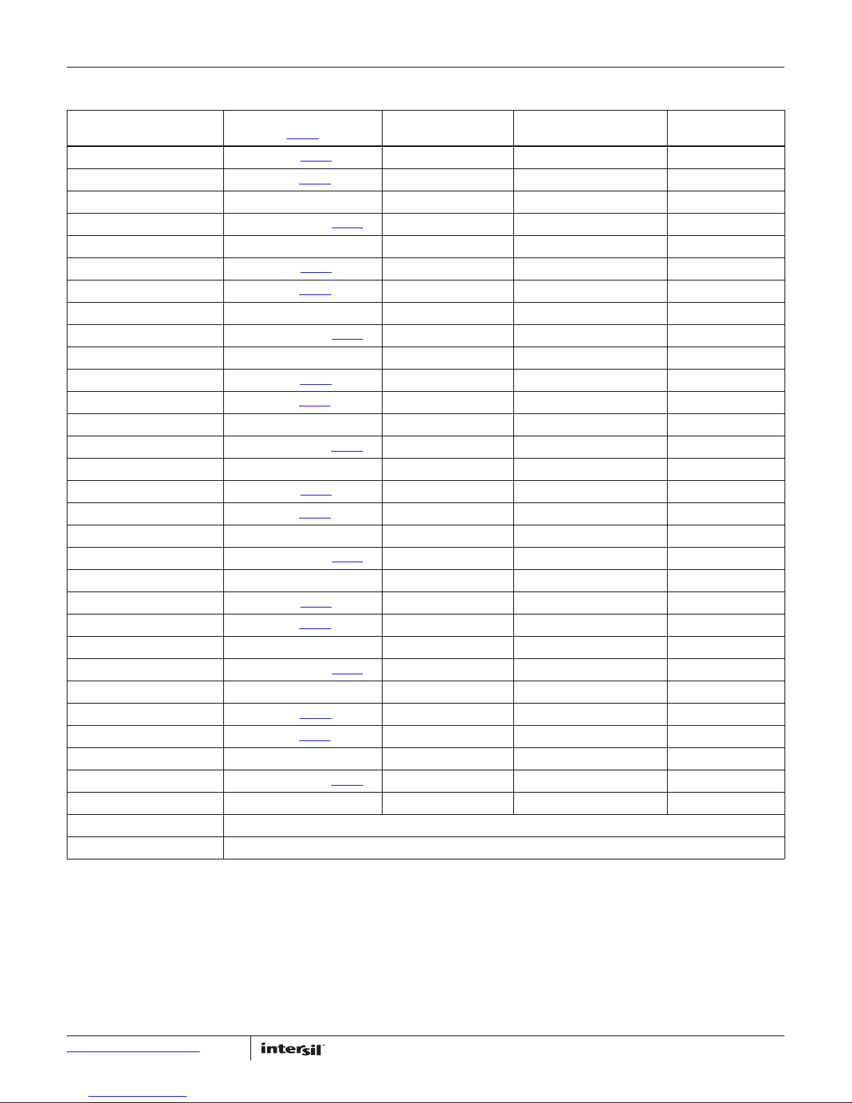
Ordering Information
ORDERING NUMBER
5962R1121301QXC ISL705ARHQF (Note 2
5962R1121301VXC ISL705ARHVF (Note 2
5962R1121301V9A ISL705ARHVX -55 to +125 Die
ISL705ARHF/PROTO ISL705ARHF/PROTO (Note 2
ISL705ARHX/SAMPLE ISL705ARHX/SAMPLE -55 to +125 Die
5962R1121302QXC ISL705BRHQF (Note 2
5962R1121302VXC ISL705BRHVF (Note 2
5962R1121302V9A ISL705BRHVX -55 to +125 Die
ISL705BRHF/PROTO ISL705BRHF/PROTO (Note 2
ISL705BRHX/SAMPLE ISL705BRHX/SAMPLE -55 to +125 Die
5962R1121303QXC ISL705CRHQF (Note 2
5962R1121303VXC ISL705CRHVF (Note 2) -55 to +125 8 Ld Flatpack K8.A
5962R1121303V9A ISL705CRHVX -55 to +125 Die
ISL705CRHF/PROTO ISL705CRHF/PROTO (Note 2
ISL705CRHX/SAMPLE ISL705CRHX/SAMPLE -55 to +125 Die
5962R1121304QXC ISL706ARHQF (Note 2
5962R1121304VXC ISL706ARHVF (Note 2
5962R1121304V9A ISL706ARHVX -55 to +125 Die
ISL706ARHF/PROTO ISL706ARHF/PROTO (Note 2
ISL706ARHX/SAMPLE ISL706ARHX/SAMPLE -55 to +125 Die
5962R1121305QXC ISL706BRHQF (Note 2
5962R1121305VXC ISL706BRHVF (Note 2) -55 to +125 8 Ld Flatpack K8.A
5962R1121305V9A ISL706BRHVX -55 to +125 Die
ISL706BRHF/PROTO ISL706BRHF/PROTO (Note 2
ISL706BRHX/SAMPLE ISL706BRHX/SAMPLE -55 to +125 Die
5962R1121306QXC ISL706CRHQF (Note 2
5962R1121306VXC ISL706CRHVF (Note 2
5962R1121306V9A ISL706CRHVX -55 to +125 Die
ISL706CRHF/PROTO ISL706CRHF/PROTO (Note 2
ISL706CRHX/SAMPLE ISL706CRHX/SAMPLE -55 to +125 Die
ISL705XRHEVAL1Z ISL705XRH Evaluation Board
ISL706XRHEVAL1Z ISL706XRH Evaluation Board
NOTES:
1. Specifications for Rad Hard QML devices are controlled by the Defense Logistics Agency Land and Maritime (DLA). The SMD numbers listed in the
“Ordering Information” table must be used when ordering.
2. These Intersil Pb-free Hermetic packaged products employ 100% Au plate - e4 termination finish, which is RoHS compliant and compatible with both
SnPb and Pb-free soldering operations.
PART NUMBER
(Note 1)
) -55 to +125 8 Ld Flatpack K8.A
) -55 to +125 8 Ld Flatpack K8.A
) -55 to +125 8 Ld Flatpack K8.A
) -55 to +125 8 Ld Flatpack K8.A
) -55 to +125 8 Ld Flatpack K8.A
) -55 to +125 8 Ld Flatpack K8.A
) -55 to +125 8 Ld Flapack K8.A
) -55 to +125 8 Ld Flatpack K8.A
) -55 to +125 8 Ld Flapack K8.A
) -55 to +125 8 Ld Flatpack K8.A
) -55 to +125 8 Ld Flatpack K8.A
) -55 to +125 8 Ld Flatpack K8.A
) -55 to +125 8 Ld Flatpack K8.A
) -55 to +125 8 Ld Flatpack K8.A
) -55 to +125 8 Ld Flatpack K8.A
) -55 to +125 8 Ld Flatpack K8.A
TEMP RANGE
(°C)
PACKAGE
(RoHs Compliant)
PKG.
DWG. #
Submit Document Feedback
2
FN7662.3
February 10, 2015
Page 3
ISL705ARH, ISL705BRH, ISL705CRH, ISL706ARH, ISL706BRH, ISL706CRH
1
2
3
4
8
7
6
5
V
DD
GND
PFI
WDO
RST
WDI
PFO
MR
1
2
3
4
8
7
6
5
V
DD
GND
PFI
WDO
RST
WDI
PFO
MR
1
2
3
4
8
7
6
5
V
DD
GND
PFI
WDO
RST_OD
WDI
PFO
MR
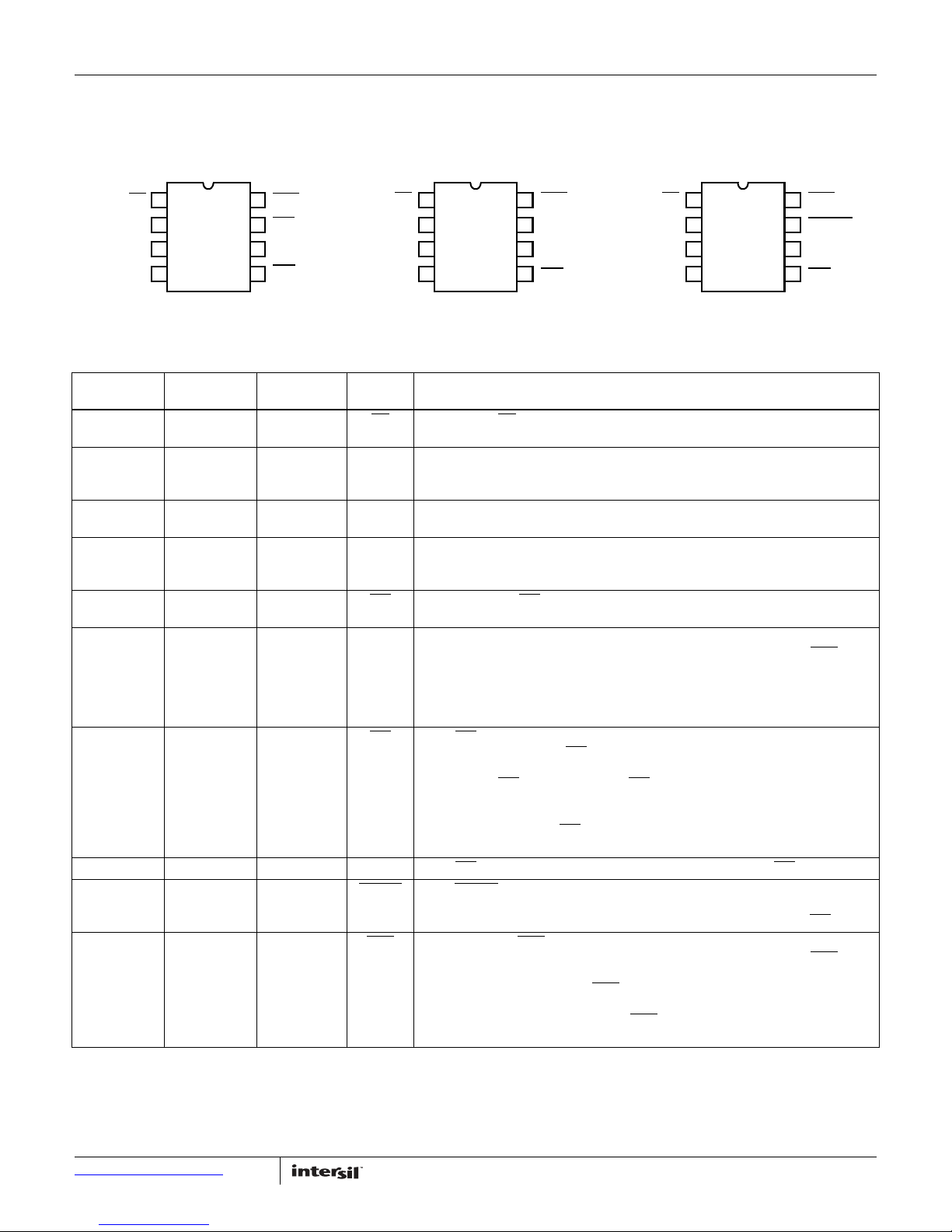
Pin Configurations
ISL705ARH, ISL706ARH
(8 LD FLATPACK)
TOP VIEW
Pin Descriptions
ISL705BRH, ISL706BRH
(8 LD FLATPACK)
TOP VIEW
ISL705CRH, ISL706CRH
(8 LD FLATPACK)
TOP VIEW
ISL705ARH
ISL706ARH
111MR
ISL705BRH
ISL706BRH
ISL705CRH
ISL706CRH
PIN
NAME DESCRIPTION
Manual Reset. MR is an active-low, debounced, TTL/CMOS compatible input that may
be used to trigger a reset pulse.
222V
Power Supply. V
DD
This input is also monitored and used to trigger a reset pulse. Reset is guaranteed
operable after V
is a supply voltage input that provides power to all internal circuitry.
DD
rises above 1.2V.
DD
333GNDGround. GND is a supply voltage return for all internal circuitry. This return establishes
the reference level for voltage detection and should be connected to signal ground.
444PFIPower Fail Input. PFI is an input to a threshold detector, which may be used to monitor
another supply voltage level. The threshold of the detector (V
ISL705ARH/BRH/CRH and 0.6V in the ISL706ARH/BRH/CRH.
555PFO
Power Fail Output. PFO is an active-low, push-pull output of a threshold detector that
indicates the voltage at the PFI pin is less than V
PFI
.
) is 1.25V in the
PFI
666WDIWatchdog Input. WDI is a tri-state input that monitors microprocessor activity. If the
microprocessor does not toggle WDI within 1.6s and WDI is not tri-stated, WDO
lo w. As lon g a s r es et is a ss er te d o r W DI i s tri-stated, the watchdog timer will stay cleared
and will not count. As soon as reset is released and WDI is driven high or low, the timer
will start counting. Floating WDI or connecting WDI to a high impedance tri-state buffer
disables the watchdog feature.
7--RST
Reset. RST is an active-low, push-pull output that is guaranteed to be low once VDD
reaches 1.2V. As V
rises, RST stays low. When VDD rises above a 4.65V
DD
(ISL705ARH/BRH/CRH) or 3.08V (ISL706ARH/BRH/CRH) reset threshold, an internal
timer releases RST
after about 200ms. RST pulses low whenever VDD goes below the
reset threshold. If a brownout condition occurs in the middle of a previously initiated
reset pulse, the pulse will continue for at least 140ms. On power-down, once V
below the reset threshold, RST
goes low and is guaranteed low until VDD drops below
1.2V.
-7-RSTReset. RST
--7RST_OD
Reset. RST_OD i s an act ive -low, ope n-d rai n ou tpu t th at g oes low whe n re set is a sse rte d.
This pin may be pulled up to V
current specifications of the output. Behavior is otherwise identical to the RST
888WDO
Watchdog Output. WDO is an active-low, push-pull output that goes low if the
is an active-high, push-pull output. RST is the inverse of RST.
with a resistor consistent with the sink and leakage
DD
microprocessor does not toggle WDI within 1.6s and WDI is not tri-stated. WDO
usually connected to the non-maskable interrupt input of a microprocessor. When V
drops below the reset threshold, WDO
will go low whether or not the watchdog timer
has timed out. Reset is simultaneously asserted, thus preventing an interrupt. Since
floating WDI disables the internal timer, WDO
goes low only when VDD drops below the
reset threshold, thus functioning as a low line output.
goes
DD
pin.
is
falls
DD
Submit Document Feedback
3
FN7662.3
February 10, 2015
Page 4
ISL705ARH, ISL705BRH, ISL705CRH, ISL706ARH, ISL706BRH, ISL706CRH
+
V
REF
V
DD
POR
GND
WDT
V
REF
PFI
WDI
PB
WDO
PF
PFO
MR
RST
ISL705ARH, ISL706ARH
V
REF
V
DD
POR
GND
WDT
V
REF
PFI
WDI
PB
WDO
PF
PFO
MR
RST
ISL705BRH, ISL706BRH
ISL705CRH, ISL706CRH
V
REF
V
DD
POR
GND
WDT
V
REF
PFI
WDI
PB
WDO
PF
PFO
MR
RST_OD
-
+
-
+
-
+
-
+
-
+
-
V
DD
MR
RST
t
RST
V
RST
1.2V
t
RST
t
RST
>t
MR
RST
<t
MD
V
DD
WDI
WDO
V
RST
1.2V
t
WD
>t
WP
< t
WD
< t
WD
< t
WD
t
RST
RST
t
RST
t
WD
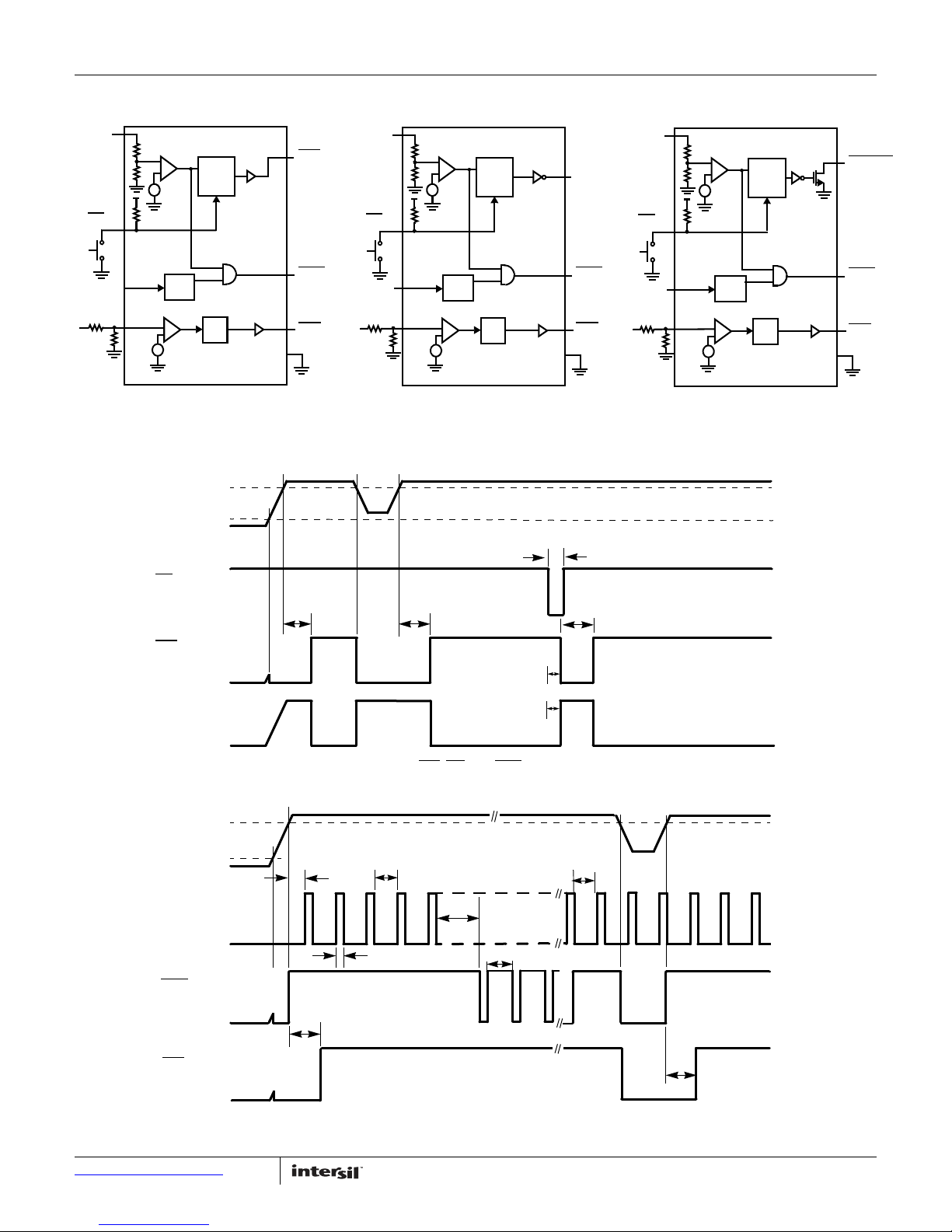
Functional Block Diagrams
Timing Diagrams
Submit Document Feedback
4
FIGURE 3. RST, RST, MR AND WDO TIMING DIAGRAM
FIGURE 4. WATCHDOG TIMING DIAGRAM
FN7662.3
February 10, 2015
Page 5
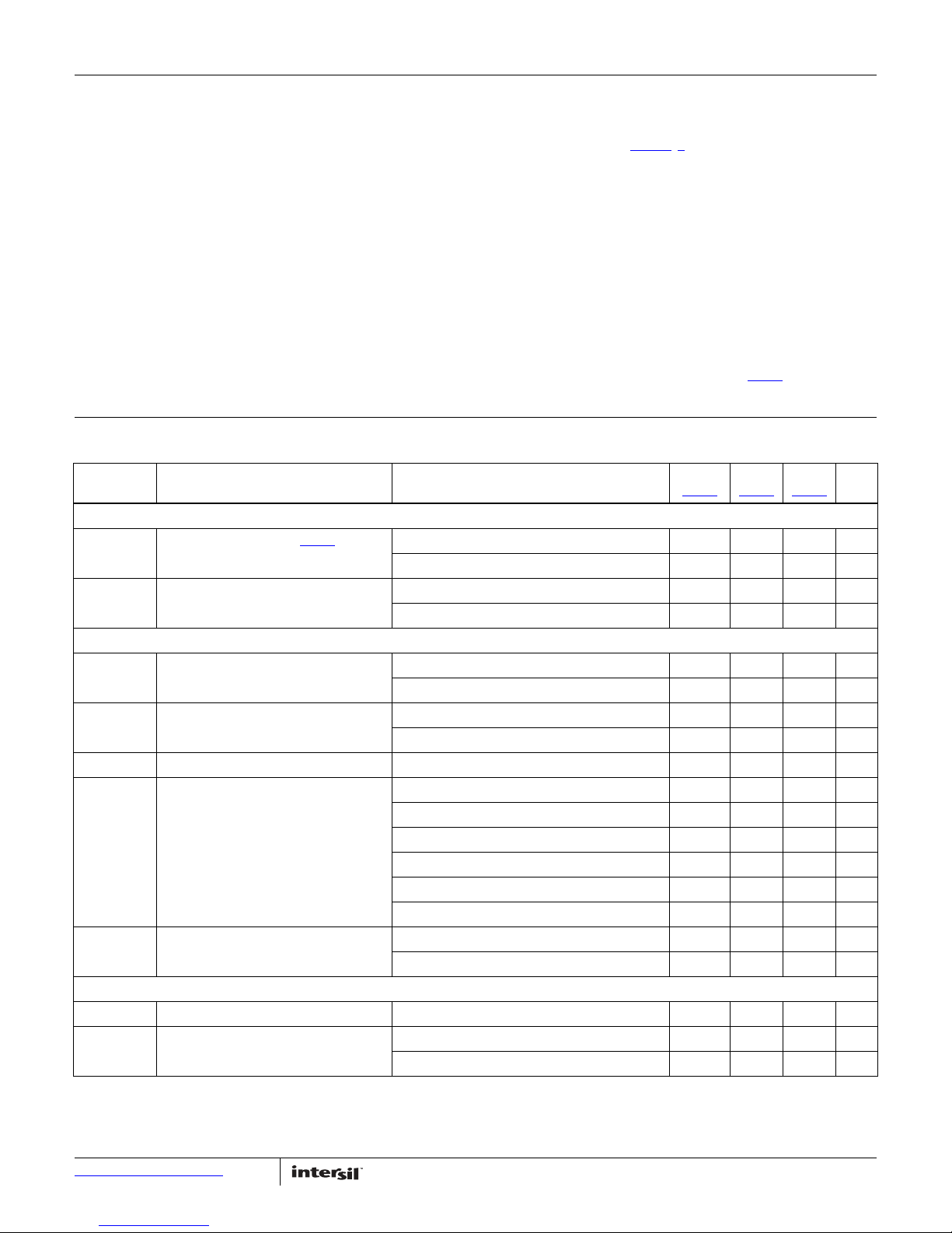
ISL705ARH, ISL705BRH, ISL705CRH, ISL706ARH, ISL706BRH, ISL706CRH
Absolute Maximum Ratings Thermal Information
Supply Voltage Range . . . . . . . . . . . . . . . . . . . . . . . . . . . . . . . . -0.3V to 6.5V
Voltage on All Other Inputs . . . . . . . . . . . . . . . . . . . . . . . -0.3V to V
ESD Rating
DD
+ 0.3V
Human Body Model (Tested per MIL-PRF-883 3015.7). . . . . . . . . .3.0kV
Machine Model (Tested per JESD22-A115C) . . . . . . . . . . . . . . . . . . 300V
Charged Device Model (Tested per JESD22-C110D) . . . . . . . . . . . .1.0kV
Latch Up (Tested per JESD-78C) . . . . . . . . . . . . . . . . . . . . . . Class 2, Level A
CAUTION: Do not operate at or near the maximum ratings listed for extended periods of time. Exposure to such conditions may adversely impact product
reliability and result in failures not covered by warranty.
NOTES:
3.
is measured with the component mounted on a low effective thermal conductivity test board in free air. See Tech Brief TB379 for details.
JA
4. For
, the “case temp” location is the center of the package underside.
JC
Thermal Resistance (Typical)
8 Ld Flatpack Package (Notes 3
, 4). . . . . . 140 15
(°C/W) JC (°C/W)
JA
Maximum Junction Temperature . . . . . . . . . . . . . . . . . . . . . . . . . . . . +175°C
Storage Temperature Range. . . . . . . . . . . . . . . . . . . . . . . .-65°C to +150°C
Recommended Operating Conditions
Temperature . . . . . . . . . . . . . . . . . . . . . . . . . . . . . . . . . . . . .-55°C to +125°C
Supply Voltage
ISL705ARH/BRH/CRH . . . . . . . . . . . . . . . . . . . . . . . . . . . . . 4.75V to 5.5V
ISL706ARH/BRH/CRH . . . . . . . . . . . . . . . . . . . . . . . . . . . . . 3.15V to 3.6V
Electrical Specifications Unless otherwise specified V
ISL706ARH/BRH/CRH T
= -55°C to +125°C. Boldface limits apply across the ambient operating temperature range, -55°C to +125°C.
A
= 4.75V to 5.5V for the ISL705ARH/BRH/CRH, V
DD
SYMBOL PARAMETER TEST CONDITIONS
POWER SUPPLY SECTION
V
DD
Operating Supply Voltage (Note 7) ISL705ARH/BRH/CRH 1.2 5 5.5 V
ISL706ARH/BRH/CRH 1.2 3.3 3.6 V
I
DD
Operating Supply Current ISL705ARH/BRH/CRH 530 µA
ISL706ARH/BRH/CRH 400 µA
RESET SECTION
V
RST
Reset Threshold Voltage ISL705ARH/BRH/CRH 4.50 4.65 4.75 V
ISL706ARH/BRH/CRH 3.00 3.08 3.15 V
V
HYS
Reset Threshold Voltage Hysteresis ISL705ARH/BRH/CRH 20 40 mV
ISL706ARH/BRH/CRH 20 30 mV
V
t
RST
OUT
Reset Pulse Width 140 200 280 ms
Reset Output Voltage ISL705ARH/BRH, I
ISL705ARH/BRH/CRH, I
ISL706ARH/BRH, I
ISL706ARH/BRH/CRH, I
ISL70XARH/CRH, V
SOURCE
SOURCE
= 1.2V, I
DD
SINK
SINK
ISL70XBRH, VDD = 1.2V, I
I
LEAK
Reset Output Leakage Current ISL705CRH, V
ISL706CRH, V
OUT
OUT
= V
= V
DD
DD
WATCHDOG SECTION
t
t
WD
WP
Watchdog Time-out Period 1.00 1.60 2.25 s
Watchdog Input (WDI) Pulse Width ISL705ARH/BRH/CRH, VIL=0.4V, VIH = 0.8 x V
ISL706ARH/BRH/CRH, V
IL
= 3.15V to 3.6V for the
DD
MIN
(Note 5
)
TYP
(Note 6)
MAX
(Note 5)UNITS
= 800µA VDD - 1.5 V
= 3.2mA 0.4 V
= 500µA 0.8 x V
DD
= 1.2mA 0.3 V
= 100µA 0.3 V
SINK
= 4µA 0.9 V
SOURCE
1 µA
1 µA
50 ns
100 ns
=0.4V, VIH = 0.8 x V
DD
DD
V
Submit Document Feedback
5
FN7662.3
February 10, 2015
Page 6
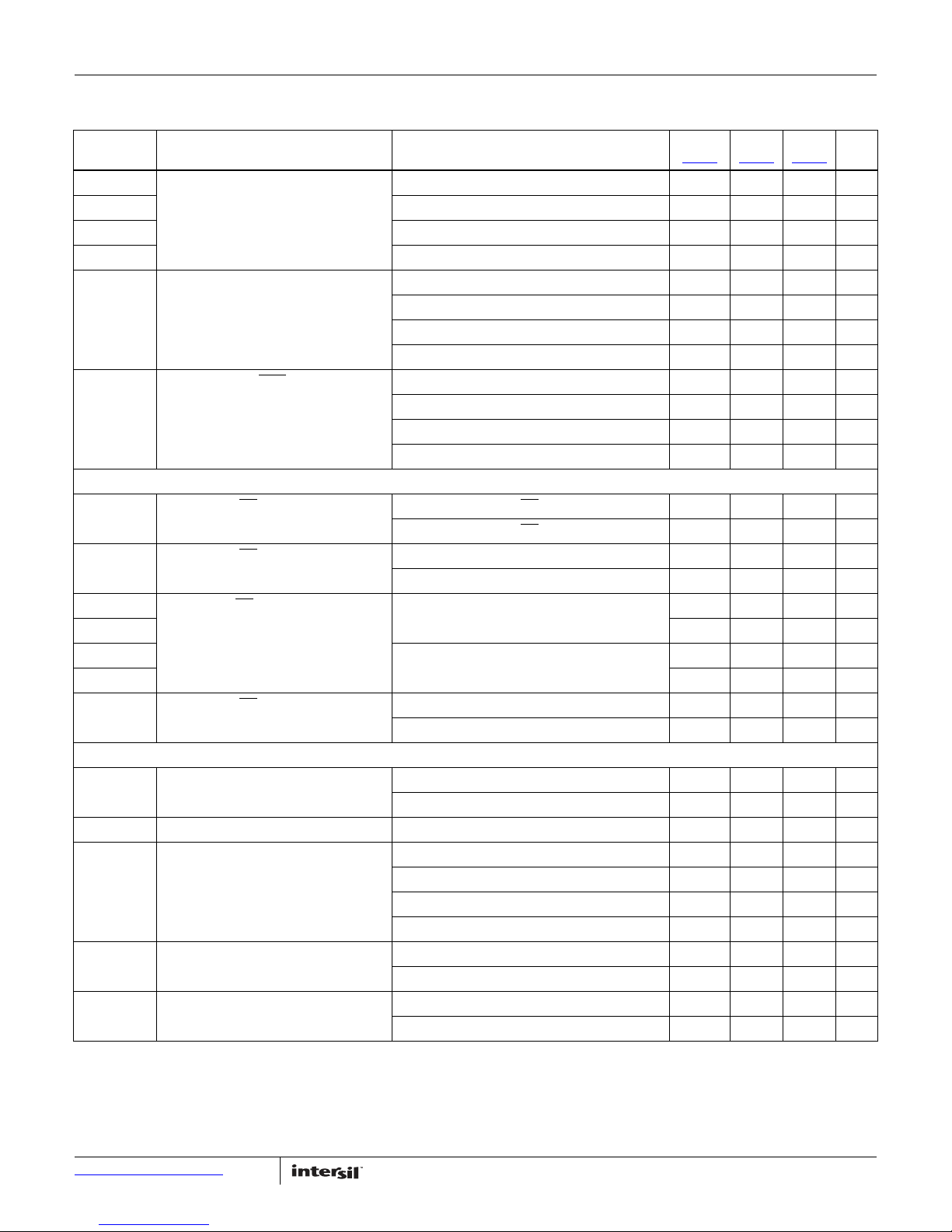
ISL705ARH, ISL705BRH, ISL705CRH, ISL706ARH, ISL706BRH, ISL706CRH
Electrical Specifications Unless otherwise specified V
ISL706ARH/BRH/CRH T
SYMBOL PARAMETER TEST CONDITIONS
V
V
V
V
I
WDI
Watchdog Input (WDI) Threshold Voltage ISL705ARH/BRH/CRH 0.8 V
IL
IH
IL
IH
Watchdog Input (WDI) Current ISL705ARH/BRH/CRH, WDI = V
= -55°C to +125°C. Boldface limits apply across the ambient operating temperature range, -55°C to +125°C. (Continued)
A
ISL705ARH/BRH/CRH 3.5 V
ISL706ARH/BRH/CRH 0.6 V
ISL706ARH/BRH/CRH 0.7 x V
= 4.75V to 5.5V for the ISL705ARH/BRH/CRH, V
DD
DD
(Note 5
ISL705ARH/BRH/CRH, WDI = 0V -100 µA
ISL706ARH/BRH/CRH, WDI = V
DD
ISL706ARH/BRH/CRH, WDI = 0V -5 µA
V
WDO
Watchdog Output (WDO) Voltage ISL705ARH/BRH/CRH, I
ISL705ARH/BRH/CRH, I
ISL706ARH/BRH/CRH, I
ISL706ARH/BRH/CRH, I
= 800µA VDD - 1.5 V
SOURCE
= 1.2mA 0.4 V
SINK
= 500µA 0.8 x V
SOURCE
= 500µA 0.3 V
SINK
MANUAL RESET SECTION
I
MR
Manual Reset (MR) Pull-up Current ISL705ARH/BRH/CRH, MR =0V -500 -100 µA
ISL706ARH/BRH/CRH, MR =0V -250 -25 µA
t
MR
Manual Reset (MR) Pulse Width ISL705ARH/BRH/CRH 150 ns
ISL706ARH/BRH/CRH 150 ns
V
V
V
V
t
MD
Manual Reset (MR) Input Threshold Voltage ISL705ARH/BRH/CRH 0.8 V
IL
IH
IL
IH
ISL706ARH/BRH/CRH 0.6 V
0.7 x V
Manual Reset (MR) to Reset Out Delay ISL705ARH/BRH/CRH 100 ns
ISL706ARH/BRH/CRH 100 ns
THRESHOLD DETECTOR SECTION
V
I
V
t
RPFI
PFI
PFI
PFO
Power Fail Input (PFI) Input Threshold
Voltage
ISL705ARH/BRH/CRH 1.20 1.25 1.30 V
ISL706ARH/BRH/CRH 0.576 0.6 0.624 V
Power Fail Input (PFI) Input Current -10 10 nA
Power Fail Output (PFO) Output Voltage ISL705ARH/BRH/CRH, I
ISL705ARH/BRH/CRH, I
ISL706ARH/BRH/CRH, I
ISL706ARH/BRH/CRH, I
= 800µA VDD - 1.5 V
SOURCE
= 3.2mA 0.4 V
SINK
= 500µA 0.8 x V
SOURCE
= 1.2mA 0.3 V
SINK
PFI Rising Threshold Crossing to PFO Delay ISL705ARH/BRH/CRH 7 15 µs
ISL706ARH/BRH/CRH 11 20 µs
t
FPFI
PFI Falling Threshold Crossing to PFO Delay ISL705ARH/BRH/CRH 20 35 µs
ISL706ARH/BRH/CRH 25 40 µs
NOTES:
5. Compliance to datasheet limits is assured by one or more methods: production test, characterization and/or design.
6. Typical values shown reflect T
= TJ = +25°C operation and are not guaranteed.
A
7. Reset is the only parameter operable within 1.2V and the minimum recommended operating supply voltage.
= 3.15V to 3.6V for the
DD
MIN
)
DD
TYP
(Note 6)
MAX
(Note 5)UNITS
100 µA
5 µA
DD
2.0 V
DD
DD
V
V
V
V
Submit Document Feedback
6
FN7662.3
February 10, 2015
Page 7
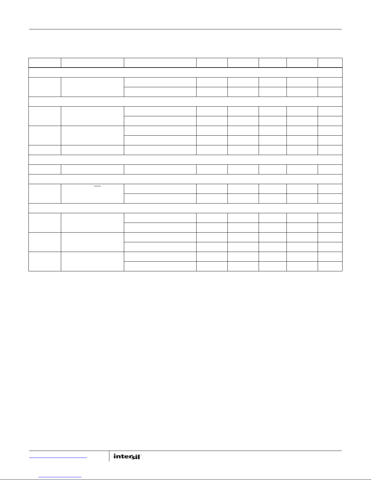
ISL705ARH, ISL705BRH, ISL705CRH, ISL706ARH, ISL706BRH, ISL706CRH
Post Radiation Characteristics Unless otherwise specified, V
for the ISL706ARH/BRH/CRH T
show typical parameter shifts due to high dose radiation. These are not limits nor are they guaranteed.
SYMBOL PARAMETER CONDITIONS 0 - 25kRad 0 - 50kRad 0 - 75kRad 0 - 100kRad UNITS
POWER SUPPLY SECTION
I
DD
RESET SECTION
V
RST
V
HYS
t
RST
WATCHDOG SECTION
t
WD
MANUAL RESET SECTION
t
MD
THRESHOLD DETECTOR SECTION
V
PFI
t
RPFI
t
FPFI
Operating Supply Current ISL705ARH/BRH/CRH -2 -2.44 -3.86 -4.88 µA
Reset Threshold Voltage ISL705ARH/BRH/CRH -8.1 -13.1 -17.5 -18.1 mV
Reset Threshold Voltage
Hysteresis
Reset Pulse Width -2.13 -2.18 -2.39 -2.35 ms
Watchdog Time-Out Period -56 -72 -81 -80 ms
Manual Reset (MR) to Reset
Out Delay
Power Fail Input (PFI) Input
Threshold Voltage
PFI Rising Threshold
Crossing to PFO Delay
PFI Falling Threshold
Crossing to PFO Delay
= +25°C. This data is parameter deltas post radiation exposure at a rate of 50 to 300rad(Si)/s. This data is intended to
A
ISL706ARH/BRH/CRH -4.79 -7.47 -6.93 -8.88 µA
ISL706ARH/BRH/CRH -1 -3.25 -5.38 -7.25 mV
ISL705ARH/BRH/CRH -3.75 -1.9 -5 -3.12 mV
ISL706ARH/BRH/CRH 0.375 0.25 0.625 0.625 mV
ISL705ARH/BRH/CRH 0.028 0.146 0.274 0.368 ns
ISL706ARH/BRH/CRH 0.305 0.605 0.793 0.956 ns
ISL705ARH/BRH/CRH 0.94 0.31 0 -0.62 mV
ISL706ARH/BRH/CRH -1.56 -2.5 -2.5 -2.5 mV
ISL705ARH/BRH/CRH -0.026 -0.047 -0.085 -0.068 µs
ISL706ARH/BRH/CRH 0.028 -0.058 0.11 -0.11 µs
ISL705ARH/BRH/CRH -0.397 -0.77 -1.17 -2.88 µs
ISL706ARH/BRH/CRH -0.35 -0.782 -1.516 -2.087 µs
= 4.75V to 5.5V for the ISL705ARH/BRH/CRH, V
DD
= 3.15V to 3.6V
DD
Submit Document Feedback
7
FN7662.3
February 10, 2015
Page 8
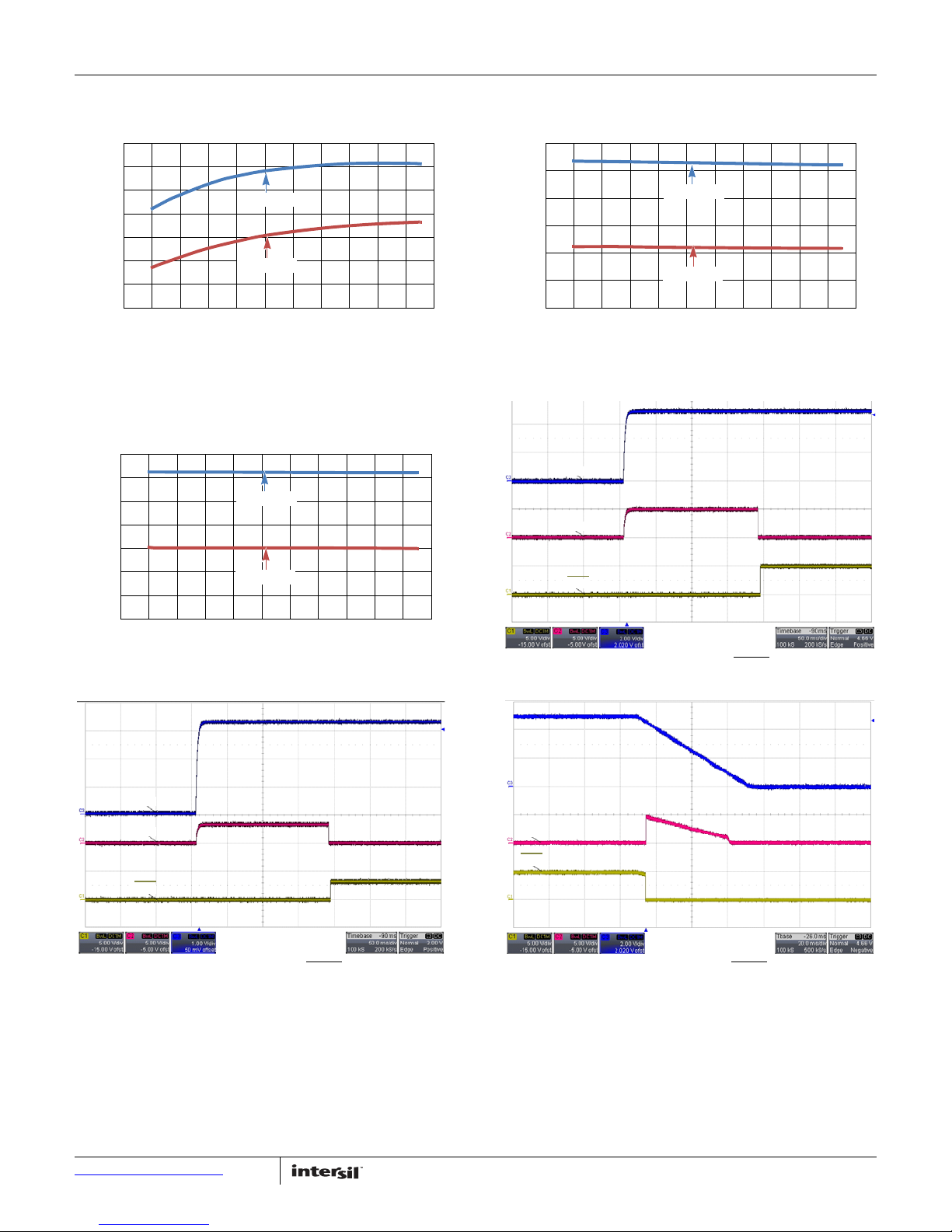
ISL705ARH, ISL705BRH, ISL705CRH, ISL706ARH, ISL706BRH, ISL706CRH
200
250
300
350
400
450
500
550
-80 -60 -40 -20 0 20 40 60 80 100 120 140
TEMPERATURE (°C)
I
DD
(µA)
ISL705xRH
ISL706xRH
2.0
2.5
3.0
3.5
4.0
4.5
5.0
-80 -60 -40 -20 0 20 40 60 80 100 120 140
V
RST
(V)
TEMPERATURE (°C)
ISL705xRH
ISL706xRH
0
0.2
0.4
0.6
0.8
1.0
1.2
1.4
-80 -60 -40 -20 0 20 40 60 80 100 120 140
TEMPERATURE (°C)
V
PFI
(V)
ISL705xRH
ISL706xRH
VDD
RST
RST
VDD
RST
RST
VDD
RST
RST
Typical Performance Curves
FIGURE 5. IDD vs TEMPERATURE FIGURE 6. V
FIGURE 7. V
vs TEMPERATURE FIGURE 8. ISL705xRH RESET and RESET ASSERTION
PFI
vs TEMPERATURE
RST
FIGURE 9. ISL706xRH RESET AND RESET
Submit Document Feedback
8
ASSERTION FIGURE 10. ISL705xRH RESET AND RESET DEASSERTION
FN7662.3
February 10, 2015
Page 9
ISL705ARH, ISL705BRH, ISL705CRH, ISL706ARH, ISL706BRH, ISL706CRH
VDD
RST
RST
PFO
PFI
PFI
PFO
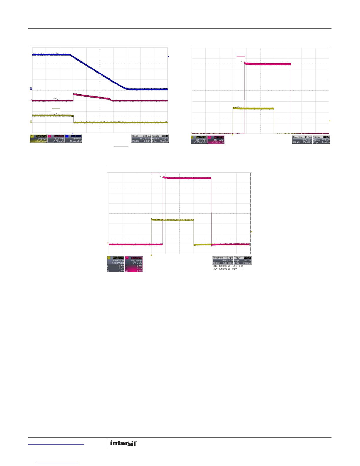
Typical Performance Curves (Continued)
FIGURE 11. ISL706xRH RESET AND RESET DEASSERTION FIGURE 12. ISL705xRH PFI TO PFO RESPONSE
Submit Document Feedback
FIGURE 13. ISL706xRH PFI TO PFO RESPONSE
9
FN7662.3
February 10, 2015
Page 10
ISL705ARH, ISL705BRH, ISL705CRH, ISL706ARH, ISL706BRH, ISL706CRH
V
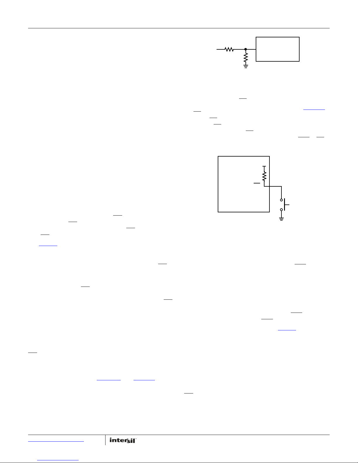
INVPFI
R1 R2+
R2
----------------------
=
(EQ. 1)
FIGURE 14. CUSTOM VTH WITH RESISTOR DIVIDER ON PFI
V
IN
R1
R2
PFI
ISL705xRH/ISL706xRH
MR
PB
20k
FIGURE 15. CONNECTING A MANUAL RESET PUSH-BUTTON
ISL705xRH/ISL706xRH
Functional Overview
The ISL705xRH and ISL706xRH provide the functions needed for
monitoring critical voltages in high reliability applications such as
microprocessor systems. Functions of the these supervisors include
power-on reset control; supply voltage supervisions; power-fail
detection; manual-reset assertion and a watchdog timer. The
integration of all these functions along with their high threshold
accuracy, low power consumption and radiation tolerance make
these devices ideal for critical supply monitoring.
Reset Output
Reset control has long been a critical aspect of embedded
control design. Microprocessors require a reset signal during
power-up to ensure that the system environment is stable before
initialization.
The reset signal provides several benefits:
• It prevents the system microprocessor from starting to operate
with insufficient voltage.
• It prevents the processor from operating prior to stabilization
of the oscillator.
• It ensures that the monitored device is held out of operation
until internal registers are initialized.
• It allows time for an FPGA to perform its self configuration
prior to initialization of the circuit.
On power-up, once V
low. As VDD rises, RST stays low. When VDD rises above the reset
threshold (V
(typ). RST
RST
pulses low whenever VDD degrades to below V
(see Figure 3). If a brownout condition occurs in the middle of a
previously initiated reset pulse, the pulse is lengthened 200ms
(typ).
On power-down, once V
stays low and is guaranteed to be low until VDD drops below 1.2V.
The ISL705BRH and ISL706BRH active-high RST output is simply
the complement of the RST
with VDD down to 1.2V. The ISL705CRH and ISL706CRH
active-low open-drain reset output is functionally identical to RST
Power Failure Monitor
Besides monitoring V
Power Failure Monitor feature that supervises an additional
critical voltage on the Power-Fail Input (PFI) pin. For example, the
PFI pin could be used to provide an early power-fail warning,
overvoltage detection or monitor a power supply other than V
goes low whenever PFI is less than V
PFO
The threshold detector can be adjusted using an external resistor
divider network to provide custom voltage monitoring for voltages
greater than V
Submit Document Feedback
PFI
reaches 1.2V, RST is guaranteed logic
DD
), an internal timer releases RST after 200ms
falls below the reset threshold, RST
DD
output and is guaranteed to be valid
for reset control, these devices have a
DD
, according to Equation 1 (see Figure 14).
10
PFI
.
RST
Manual Reset
The manual reset input (MR) allows designers to add manual
system reset capability via a push button switch (see Figure 15).
input is an active low debounced input which asserts
The MR
reset if the MR pin is pulled low to less than VIL for at least
150ns. After MR is released, the reset output remains asserted
and then released. MR is a TTL/CMOS logic compatible,
for t
RST
so it can be driven by external logic. By connecting WDO to MR,
one can force a watchdog time out to generate a reset pulse.
Watchdog Timer
The watchdog time circuit checks for coherent program
execution by monitoring the WDI pin. If the processor does not
toggle the watchdog input within tWD (1.0s min), WDO will go
low. As long as reset is asserted or the WDI pin is tri-stated, the
watchdog timer will stay cleared and not count. As soon as reset
is released and WDI is driven high or low, the timer will start
counting. Pulses as short as 50ns can be detected on the
ISL705xRH, on ISL706xRH pulses as short as 100ns can be
.
detected.
Whenever there is a low-voltage V
Unlike the reset outputs, however, WDO
rises above its voltage trip point (see Figure 4). With WDI
V
DD
condition, WDO goes low.
DD
goes high as soon as
open or connected to a tri-stated high impedance input, the
< V
RST
.
DD
watchdog timer is disabled and only pulls low when V
.
DD
Applications Information
Negative Voltage Sensing
This family of devices can be used to sense and monitor the
presence of both a positive and negative rail. VDD is used to
monitor the positive supply while PFI monitors the negative rail.
is high when the negative rail degrades below a V
PFO
and remains low when the negative rail is above the V
As the differential voltage across the R1, R2 divider is increased,
the resistor values must be chosen such that the PFI node is
<1.25V when the -V supply is satisfactory and the positive supply
February 10, 2015
TRIP
TRIP
value
value.
FN7662.3
Page 11
ISL705ARH, ISL705BRH, ISL705CRH, ISL706ARH, ISL706BRH, ISL706CRH
R2
R1 VPFI V
TRIP
–
VDD VPFI–
---------------------------------------------------
=
(EQ. 2)
R2
100k 1.25 4.5––
51.25–
----------------------------------------------------
153.3 k ==
(EQ. 3)
+5V
ISL705ARH
-5V
100k
100k
2N3904
MR
RST
PFO
PFI
R1
R2
V
DD
ISL705ARH, ISL706ARH
100kΩ
RST
V
DD
ISL705BRH, ISL706BRH
300kΩ
RST
V
DD
R1
ISL706CRH, ISL705CRH
R
PULL
RST_OD
V
DD
V
PULL
R
PULL
V
PULL
I
SINK
------------------
=
(EQ. 4)
is at its maximum specified value. This allows the positive supply
to fluctuate within its acceptable range without signaling a reset
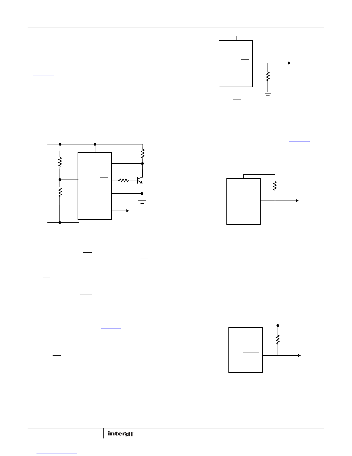
when configured as shown in Figure 16.
In Figure 16
-5V through PFI. In this example, the trip point (V
negative supply rail is set for -4.5V. Equation 2
, the ISL705ARH is monitoring +5V through VDD and
) for the
TRIP
can be used to
select the appropriate resistor values. R1 is selected arbitrarily as
100kΩ, V
= 5V, V
DD
= 1.25V and V
PFI
= (-4.5V). By plugging
TRIP
the values into Equation 2 as shown in Equation 3, it can be seen
a resistor of 153.3kΩ is needed. The closest 1% resistor value is
154kΩ.
FIGURE 16. ±5V MONITORING
Figure 4
base is connected to the PFO
also has a general purpose NPN transistor in which the
pin through a 100kΩ resistor. The
emitter is tied to ground and the collector is tied to MR signal.
This configuration allows the negative voltage sense circuit to
initiate a reset if it is not within its regulation window. A pull-up
on the MR
ensures no false reset triggering when the negative
voltage is within its regulation window.
Assuring a Valid RST Output
When VDD falls below 1.2V, the RST output can no longer sink
current and is essentially an open circuit. As a result, this pin can
drift to undetermined voltages if left undriven. By adding a pull-down
resistor to the RST
leakage currents will be drained to ground and keep RST low when
falls below 1.2V. The resistor value (R1) is not critical, however,
V
DD
it should be large enough not to load RST
RST to ground. A 100kΩ resistor would suffice, assuming there is no
load on the RST
pin as shown in Figure 17, any stray charge or
and small enough to pull
pin during that time.
FIGURE 17. RST VA LID TO GROUND CIRC UIT
Assuring a Valid RST Output
On the ISL705BRH and ISL706BRH, when VDD falls below 1.2V, the
RST output can no longer source enough current to track VDD. As a
result, this pin can drift to undetermined voltages if left undriven. By
adding a pull-up resistor to the RST pin as shown in Figure 18
will track V
below 1.2V. The resistor value (R1) is not critical,
DD
, RST
however, it should be large enough not to exceed the sink capability
of RST pin at 1.2V. A 300kΩ resistor would suffice, assuming there
is no load on the RST pin during that time.
FIGURE 18. RST VALID TO GROUND CIRCUIT
Selecting Pull-up Resistor Values
The ISL705CRH and ISL706CRH have open drain active low reset
outputs (RST_OD). A pull-up resistor is needed to ensure RST_OD
is high when VDD is in a valid state (Figure 19). The resistor value
must be chosen in order not to exceed the sink capability of the
RST_OD
the ISL706CRH has a sink capability of 1.2mA. Equation 4 may
be used to select resistor R
V
exceed V
pin. The ISL705ARH has a sink capability of 3.2mA and
based on the pull-up voltage
. It is also important that the pull-up voltage does not
PULL
DD
.
PULL
Submit Document Feedback
11
FIGURE 19. RST_OD
PULL-UP CONNECTION
FN7662.3
February 10, 2015
Page 12
ISL705ARH, ISL705BRH, ISL705CRH, ISL706ARH, ISL706BRH, ISL706CRH
ISL705ARH
RST
PFO
PFI
R1
R2
V
DD
R3
R1 R3
VHB
V
DD
-------------
124k ==
(EQ. 5)
VTR V
PFI
1
VHB
V
DD
-------------
+
(EQ. 6)
R2 1
VTR
V
PFI
R1
--------------------------------
1
R1
--------
–
1
R3
--------
–=
(EQ. 7)
VTR V
PFI
R1
1
R1
--------
1
R2
--------
1
R3
--------
++=
(EQ. 8)
VTF VTR
R1 VDD
R3
----------------------------
–=
(EQ. 9)
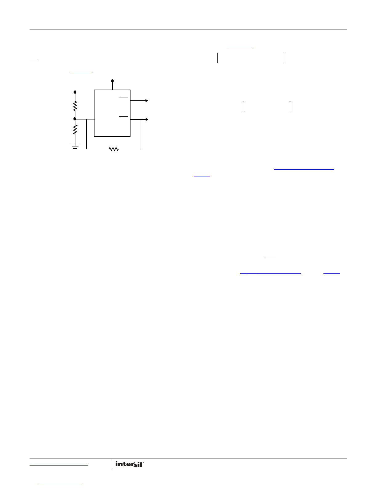
Adding Hysteresis to the PFI Comparator
The PFI comparator has no built-in hysteresis, however, the
designer may add hysteresis by connecting a resistor from the
pin to the PFI pin, essentially adding positive feedback to the
PFO
comparator (see Figure 20).
FIGURE 20. POSITIVE FEEDBACK FOR HYSTERESIS
The following procedure allows the system designer to calculate
the components based on the requirements and on given data,
such as supply rail voltages, hysteresis band voltage (VHB) and
reference voltage (V
The comparator only has two states of operation. When it is low,
the current through R3 is I
IR3 = (VDD - V
PFI
small so it does not induce oscillations; 200nA is a good starting
point. Now two values of R3 can be calculated with V
V
= 1.25V; R3 = 6.25MΩ or 11.25MΩ, select the lowest value
PFI
of the two.
With R3 selected as 6.2MΩ (closest standard 1% resistor), R1
can be calculated as:
with VHB selected at 100mV. The closest standard value for R1 is
124kΩ. Then next step is select the rising trip voltage (VTR) such
that:
).
PFI
= V
R3
/R3. When the output is high,
PFI
)/R3. The feedback current needs to be very
= 5V and
DD
The rising threshold voltage is selected at 3.0V and R2 is
calculated by Equation 7
.
Plugging in all the variables in equation 7 and solving for R2
yields 90.9kΩ. Note that the 90.9kΩ solution includes rounding
to the closest standard 1% resistor value. The final step is verify
the trip voltages.
The rising voltage, VTR, is calculated as 2.98V and the falling
voltage, VTF, is calculated as 2.88V, so 100mV hysteresis is
achieved.
An additional item to consider is that the output voltage is equal
, however, according to the “Electrical Specifications” on
to V
DD
page 6
, the output of the PFI comparator is guaranteed to be at
least (VDD-1.5) volts. When you take this worst case into account,
the hysteresis can be as low at 70mV.
Special Application Considerations
Using good decoupling practices will prevent transients (i.e., due
to switching noises and short duration droops in the supply
voltage) from causing unwanted resets and reduce the power-fail
circuit’s sensitivity to high-frequency noise on the line being
monitored.
When the WDI input is left unconnected, it is recommended to
place a 10µF capacitor to ground to reduce single event
transients from arising in the WDO
As described in the “
there is a delay on the PFO
Electrical Specifications” Tabl e on page 6,
pin whenever PFI crosses the
threshold. This delay is due to internal filters on the PFI
comparator circuitry which were added to mitigate single event
transients. If the PFI input transitions below or above the
threshold and the duration of the transition is less than the delay,
the PFO pin will not change states.
pin.
12
Submit Document Feedback
FN7662.3
February 10, 2015
Page 13
ISL705ARH, ISL705BRH, ISL705CRH, ISL706ARH, ISL706BRH, ISL706CRH
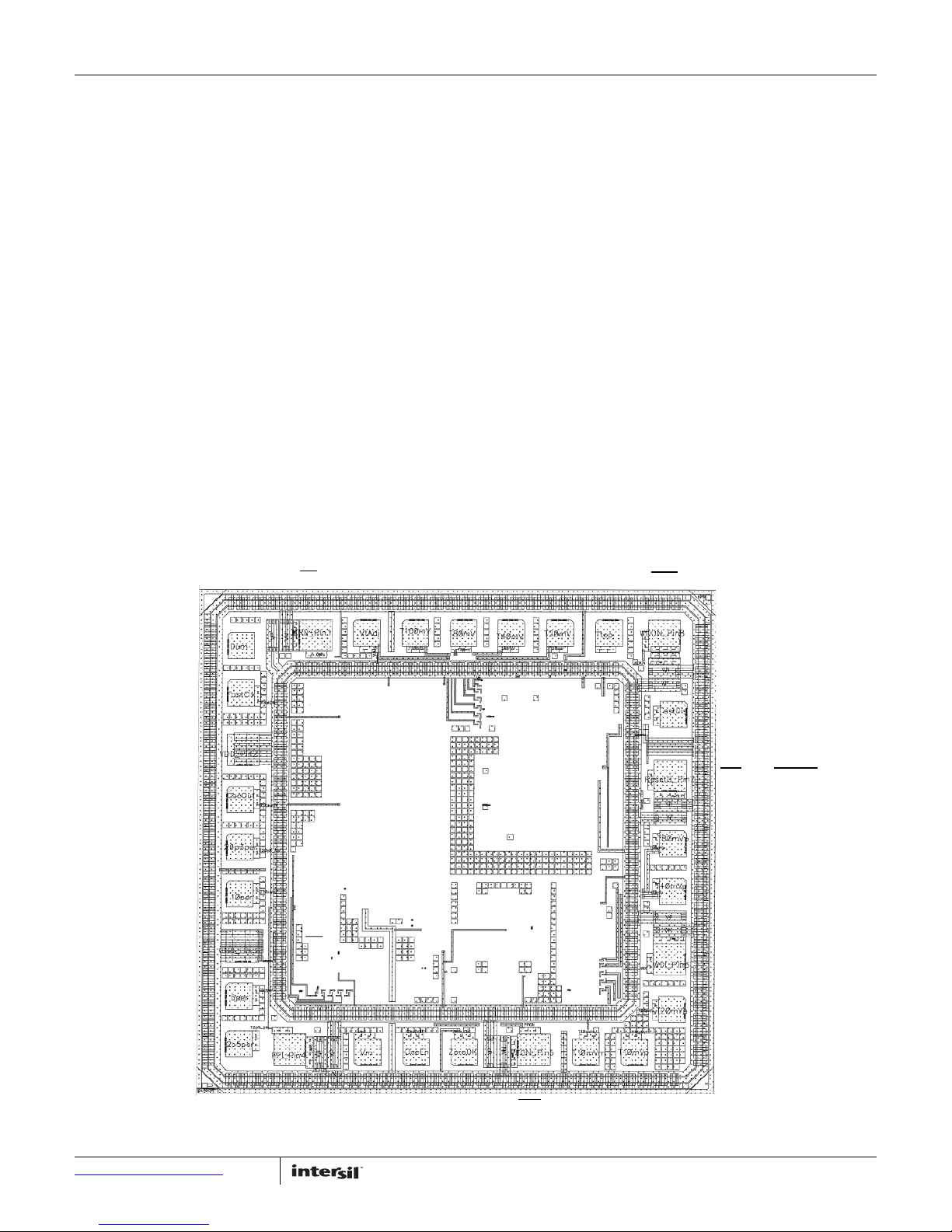
WDO
MR
VDD
GND
PFI
PFO
WDI
RST
, RST, RST_OD
Weight Characteristics
Weight of Packaged Device
0.31 Grams typical
Die Characteristics
Die Dimensions
2030µm x 2030µm (79.9 mils x 79.9 mils)
Thickness: 483µm ±25.4µm (19.0 mils ±1 mil)
Interface Materials
GLASSIVATION
Type: Silicon Oxide and Silicon Nitride
Thickness: 0.3µm ±0.03µm to 1.2µm ±0.12µm
TOP METALLIZATION
Type: AlCu (99.5%/0.5%)
Thickness: 2.7µm ±0.4µm
TOP METALLIZATION
Type: Silicon
BACKSIDE FINISH
Silicon
PROCESS
0.6µM BiCMOS Junction Isolated
ASSEMBLY RELATED INFORMATION
Substrate Potential
Unbiased
ADDITIONAL INFORMATION
Worst Case Current Density
5
2
< 2 x 10
Transistor Count
1400
A/cm
Layout Characteristics
Step and Repeat
2030µm x 2030µm
Metallization Mask Layout
Submit Document Feedback
13
FN7662.3
February 10, 2015
Page 14
ISL705ARH, ISL705BRH, ISL705CRH, ISL706ARH, ISL706BRH, ISL706CRH
Revision History
The revision history provided is for informational purposes only and is believed to be accurate, but not warranted. Please go to web to make sure you
have the latest Rev.
DATE REVISION CHANGE
February 10, 2015 FN7662.3 Added part number ISL706CRH to the header of pages 2 through 12, (It had been mistakenly covered up).
December 9, 2014 FN7662.2 Added SEE, ELDRS and SPICE Model reports to Related Literature on page 1.
page 2 added to Ordering Information table:
“Specifications for Rad Hard QML devices are controlled by the Defense Logistics Agency Land and Maritime (DLA).
The SMD numbers listed in the "Ordering Information" table on page 2 must be used when ordering.”
Updated POD on page 15 to most recent revision with following changes:
a) Package tkn, Changed
From: 0.115/0.070 (2.92/1.18)
To: 0.110/0.087 (2.79/2.21)
b) Bottom of lead to bottom of package, Changed
From: 0.045/0.026” (1.14/0.66)
To: 0.036/0.026 (0.92/0.66)
c) Lead length, Changed:
From: 0.370/0.250 (9.40/6.35)
To: 0.370/0.325 (9.40/8.26)
d) Lead tkn: On the side view there was a typo on lead tkn, corrected:
From: 0.09/0.04 (0.23/0.10)
To: 0.009/0.004 (0.23/0.10)
Modified Note 2 by adding the words ..."in addition to or instead of"...
November 1, 2011 FN7662.1 Page 13: Updated the transistor count to 1400 from 25000.
September 15, 2011 FN7662.0 Initial release
Pages 7, 9: Removed erroneous overline bars in Figures 8-11.
About Intersil
Intersil Corporation is a leading provider of innovative power management and precision analog solutions. The company's products
address some of the largest markets within the industrial and infrastructure, mobile computing and high-end consumer markets.
For the most updated datasheet, application notes, related documentation and related parts, please see the respective product
information page found at www.intersil.com.
You may report errors or suggestions for improving this datasheet by visiting www.intersil.com/ask
Reliability reports are also available from our website at www.intersil.com/support
.
For additional products, see www.intersil.com/en/products.html
Intersil products are manufactured, assembled and tested utilizing ISO9001 quality systems as noted
in the quality certifications found at www.intersil.com/en/support/qualandreliability.html
Intersil products are sold by description only. Intersil Corporation reserves the right to make changes in circuit design, software and/or specifications at any time
without notice. Accordingly, the reader is cautioned to verify that data sheets are current before placing orders. Information furnished by Intersil is believed to be
accurate and reliable. However, no responsibility is assumed by Intersil or its subsidiaries for its use; nor for any infringements of patents or other rights of third
parties which may result from its use. No license is granted by implication or otherwise under any patent or patent rights of Intersil or its subsidiaries.
For information regarding Intersil Corporation and its products, see www.intersil.com
Submit Document Feedback
14
FN7662.3
February 10, 2015
Page 15
ISL705ARH, ISL705BRH, ISL705CRH, ISL706ARH, ISL706BRH, ISL706CRH
LEAD FINISH
SIDE VIEW
TOP VIEW
-D-
-C-
0.265 (6.75)
0.110 (2.79)
0.026 (0.66)
0.265 (6.73)
SEATING AND
0.180 (4.57)
0.03 (0.76) MIN
BASE PLANE
-H-
0.009 (0.23)
0.005 (0.13)
PIN NO. 1
ID AREA
0.050 (1.27 BSC)
0.022 (0.56)
0.015 (0.38)
MIN
0.245 (6.22)
0.087 (2.21)
0.170 (4.32)
0.370 (9.40)
0.325 (8.26)
0.004 (0.10)
0.245 (6.22)
1.
adjacent to pin one and shall be located within the shaded area shown.
The manufacturer’s identification shall not be used as a pin one
identification mark. Alternately, a tab may be used to identify pin one.
2.
3. The maximum limits of lead dimensions (section A-A) shall be
measured at the centroid of the finished lead surfaces, when solder
dip or tin plate lead finish is applied.
4.
5.
shall be molded to the bottom of the package to cover the leads.
6.
meniscus) of the lead from the body. Dimension minimum shall
be reduced by 0.0015 inch (0.038mm) maximum when solder dip
lead finish is applied.
7.
8.
NOTES:
0.015 (0.38)
0.008 (0.20)
PIN NO. 1
ID OPTIONAL
1 2
4
6
3
Dimensioning and tolerancing per ANSI Y14.5M - 1982.
Controlling dimension: INCH.
Index area: A notch or a pin one identification mark shall be located
If a pin one identification mark is used in addition to or instead of a tab,
Measure dimension at all four corners.
For bottom-brazed lead packages, no organic or polymeric materials
Dimension shall be measured at the point of exit (beyond the
SECTION A-A
BASE
METAL
0.007 (0.18)
0.004 (0.10)
0.009 (0.23)
0.004 (0.10)
0.019 (0.48)
0.015 (0.38)
0.0015 (0.04)
MAX
0.022 (0.56)
0.015 (0.38)
0.036 (0.92)
the limits of the tab dimension do not apply.
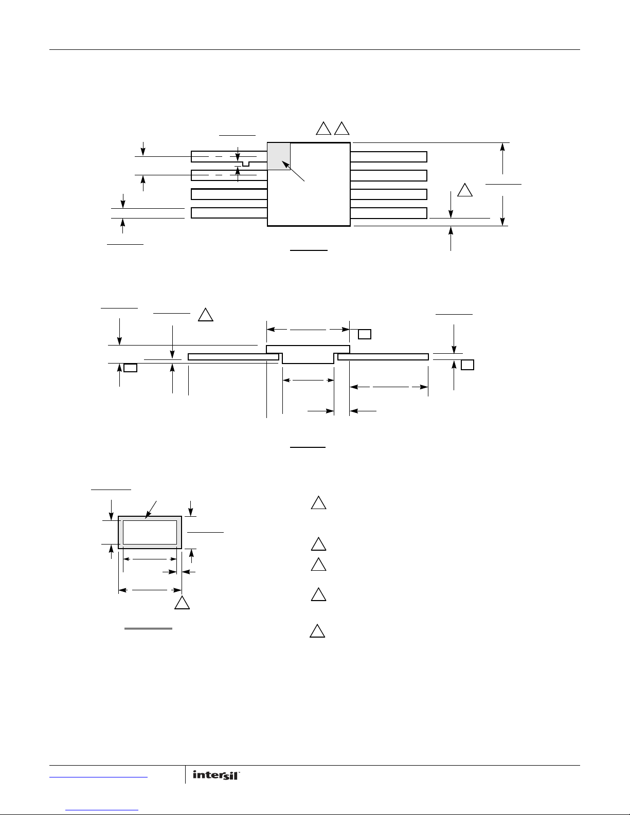
Package Outline Drawing
K8.A
8 LEAD CERAMIC METAL SEAL FLATPACK PACKAGE
Rev 4, 12/14
Submit Document Feedback
15
FN7662.3
February 10, 2015
Page 16

Mouser Electronics
Authorized Distributor
Click to View Pricing, Inventory, Delivery & Lifecycle Information:
Intersil:
ISL706XRHEVAL1Z
 Loading...