

®
www.BDTIC.com/Intersil
ISL6840, ISL6841, ISL6842,
ISL6843, ISL6844, ISL6845
Data Sheet November 12, 2007
Improved Industry Standard Single-Ended
Current Mode PWM Controller
The ISL6840, ISL6841, ISL6842, ISL6843, ISL6844,
ISL6845 family of adjustable frequency, low power, pulse
width modulating (PWM) current mode controllers is
designed for a wide range of power conversion applications
including boost, flyback, and isolated output configurations.
Peak current mode control effectively handles power
transients and provides inherent overcurrent protection.
This advanced BiCMOS design is pin compatible with the
industry standard 384x family of controllers and offers
significantly improved performance. Features include low
operating current, 60µA start-up current, adjustable
operating frequency to 2MHz, and high peak current drive
capability with 20ns rise and fall times.
PART NUMBER RISING UVLO (V) MAX. DUTY CYCLE (%)
ISL6840 7.0 100
ISL6841 7.0 50
ISL6842 14.4 100
ISL6843 8.4 100
ISL6844 14.4 50
ISL6845 8.4 50
FN9124.9
Features
• 1A MOSFET gate driver
• 60µA start-up current, 100µA maximum
• 25ns propagation delay current sense to output
• Fast transient response with peak current mode control
• Adjustable switching frequency to 2MHz
• 20ns rise and fall times with 1nF output load
• Trimmed timing capacitor discharge current for accurate
deadtime/maximum duty cycle control
• High bandwidth error amplifier
• Tight tolerance voltage reference over line, load, and
temperature
• Tight tolerance current limit threshold
• Pb-free available (RoHS Compliant)
Applications
• Telecom and Datacom Power
• Wireless Base Station Power
• File Server Power
• Industrial Power Systems
• PC Power Supplies
• Isolated Buck and Flyback Regulators
• Boost Regulators
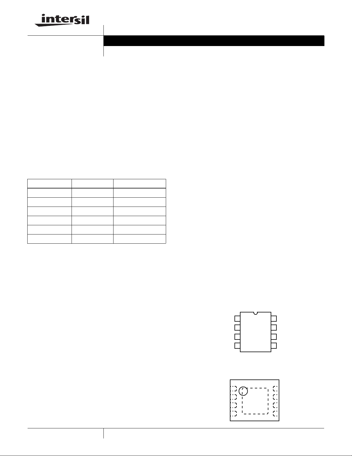
Pinout
ISL6840, ISL6841, ISL6842, ISL6843, ISL6844, ISL6845
ISL6840, ISL6841, ISL6842, ISL6843, ISL6844, ISL6845
COMP
RTCT
8 LD SOIC, MSOP
COMP
1
2
FB
3
CS
4
RTCT
1
FB
2
CS
3
4
TOP VIEW
8 LD DFN
TOP VIEW
8
7
5
6
8
7
6
5
VREF
VDD
OUT
GND
VREF
VDD
OUT
GND
1
CAUTION: These devices are sensitive to electrostatic discharge; follow proper IC Handling Procedures.
1-888-INTERSIL or 1-888-468-3774
| Intersil (and design) is a registered trademark of Intersil Americas Inc.
Copyright Intersil Americas Inc. 2004, 2005, 2007. All Rights Reserved
All other trademarks mentioned are the property of their respective owners.
ISL6840, ISL6841, ISL6842, ISL6843, ISL6844, ISL6845
www.BDTIC.com/Intersil
Ordering Information
PART NUMBER PART MARKING TEMP RANGE (°C) PACKAGE PKG. DWG. #
ISL6840IB* ISL 6840IB -40 to +105 8 Ld SOIC M8.15
ISL6840IBZ* (Note) 6840 IBZ -40 to +105 8 Ld SOIC (Pb-free) M8.15
ISL6840IRZ-T† (Note) 40Z -40 to +105 8 Ld 2x3 DFN (Pb-free) L8.2x3
ISL6840IU* 6840 -40 to +105 8 Ld MSOP M8.118
ISL6840IUZ* (Note) 6840Z -40 to +105 8 Ld MSOP (Pb-free) M8.118
ISL6841IB* ISL 6841IB -40 to +105 8 Ld SOIC M8.15
ISL6841IBZ* (Note) 6841 IBZ -40 to +105 8 Ld SOIC (Pb-free) M8.15
ISL6841IRZ-T† (Note) 41Z -40 to +105 8 Ld 2x3 DFN (Pb-free) L8.2x3
ISL6841IU* 6841 -40 to +105 8 Ld MSOP M8.118
ISL6841IUZ* (Note) 6841Z -40 to +105 8 Ld MSOP (Pb-free) M8.118
ISL6842IB* ISL 6842IB -40 to +105 8 Ld SOIC M8.15
ISL6842IBZ* (Note) 6842 IBZ -40 to +105 8 Ld SOIC (Pb-free) M8.15
ISL6842IRZ-T† (Note) 42Z -40 to +105 8 Ld 2x3 DFN (Pb-free) L8.2x3
ISL6842IU* 6842 -40 to +105 8 Ld MSOP M8.118
ISL6842IUZ* (Note) 6842Z -40 to +105 8 Ld MSOP (Pb-free) M8.118
ISL6843IB* ISL 6843IB -40 to +105 8 Ld SOIC M8.15
ISL6843IBZ* (Note) 6843 IBZ -40 to +105 8 Ld SOIC (Pb-free) M8.15
ISL6843IRZ-T† (Note) 43Z -40 to +105 8 Ld 2x3 DFN (Pb-free) L8.2x3
ISL6843IU* 6843 -40 to +105 8 Ld MSOP M8.118
ISL6843IUZ* (Note) 6843Z -40 to +105 8 Ld MSOP (Pb-free) M8.118
ISL6844IB* ISL 6844IB -40 to +105 8 Ld SOIC M8.15
ISL6844IBZ* (Note) 6844 IBZ -40 to +105 8 Ld SOIC (Pb-free) M8.15
ISL6844IRZ-T† (Note) 44Z -40 to +105 8 Ld 2x3 DFN (Pb-free) L8.2x3
ISL6844IU* 6844 -40 to +105 8 Ld MSOP M8.118
ISL6844IUZ (Note) 6844Z -40 to +105 8 Ld MSOP (Pb-free) M8.118
ISL6845IB* ISL 6845IB -40 to +105 8 Ld SOIC M8.15
ISL6845IBZ* (Note) 6845 IBZ -40 to +105 8 Ld SOIC (Pb-free) M8.15
ISL6845IRZ-T† (Note) 45Z -40 to +105 8 Ld 2x3 DFN (Pb-free) L8.2x3
ISL6845IU* 6845 -40 to +105 8 Ld MSOP M8.118
ISL6845IUZ* (Note) 6845Z -40 to +105 8 Ld MSOP (Pb-free) M8.118
*Add “-T” suffix for tape and reel. Please refer to TB347 for details on reel specifications.
†Contact Factory for Availability
NOTE: These Intersil Pb-free plastic packaged products employ special Pb-free material sets; molding compounds/die attach materials and 100%
matte tin plate PLUS ANNEAL - e3 termination finish, which is RoHS compliant and compatible with both SnPb and Pb-free soldering operations.
Intersil Pb-free products are MSL classified at Pb-free peak reflow temperatures that meet or exceed the Pb-free requirements of IPC/JEDEC J
STD-020.
2
FN9124.9
November 12, 2007
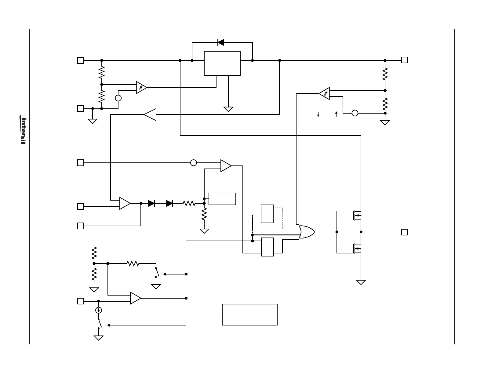
Functional Block Diagram
www.BDTIC.com/Intersil
VDD
UVLO
COMPARATOR
+
-
100mV
2R
R
ENABLE
V
OK
+
-
+
BG
3
GND
CS
FB
COMP
VREF
-
2.5V
ERROR
AMPLIFIER
+
-
DD
A
A = 0.5
V
REF
5.00V
PWM
COMPARATOR
+
-
1.1V
CLAMP
ISL6841/ISL6844/ISL6845
ONLY
Q
T
Q
SRQ
VREF FAULT
VREF
UV COMPARATOR
4.65V 4.80V
-
+
-
+
BG
VREF
ISL6840, ISL6841, ISL6842, ISL6843, ISL6844, ISL6845
OUT
2.6V
0.7V
ON
OSCILLATOR
COMPARATOR
-
RTCT
November 12, 2007
FN9124.9
8.4mA
ON
+
CLOCK
P/N
-40, -41 7.0/6.6V
-42, -44 14.3/8.8V
-43, -45
Q
RESET
DOMINANT
UVLO ON/OFF
8.4/7.2V
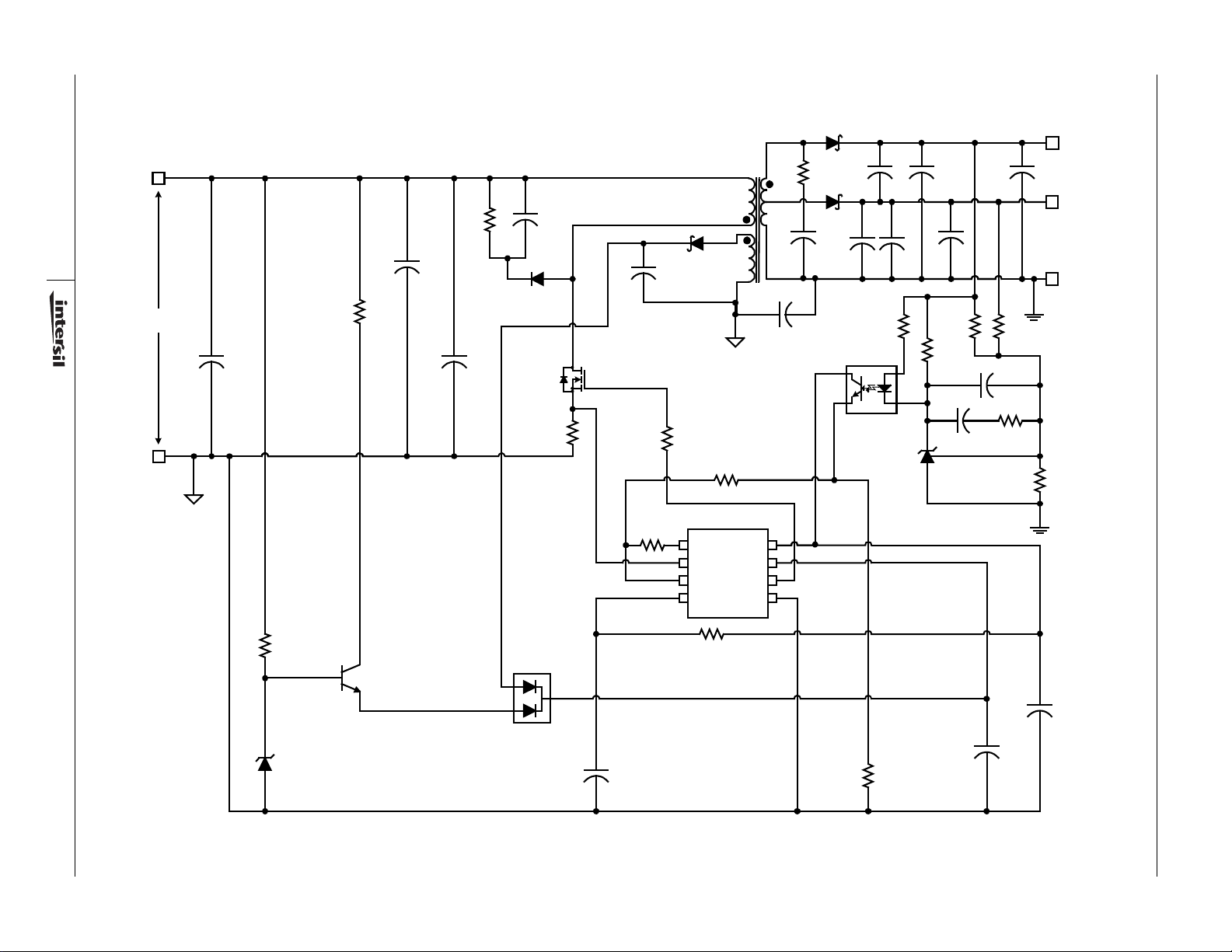
Typical Application - 48V Input Dual Output Flyback
www.BDTIC.com/Intersil
VIN+
R3
4
36V TO 75V
C1
R1
C2
C3
C4
CR6
Q1
C5
CR2
T1
C17
C6
R21
CR5
CR4
C19
C21
+
R16
U2
C15 C16
+
C22
+
C20
R17
R19
C14
R18
+3.3V
+
+1.8V
ISL6840, ISL6841, ISL6842, ISL6843, ISL6844, ISL6845
RETURN
R4
VIN-
R6
CR1
Q3
VR1
November 12, 2007
FN9124.9
C8
R26
R22
COMP
CS
FB
RTCT
ISL684x
R10
R27
U4
VREF
V
DD
OUT
GND
R13
U3
C13
R15
R20
C12
C11

Typical Application - Boost Converter
www.BDTIC.com/Intersil
VIN+
R8
L1
CR1
C10
+VOUT
+
C2
C3
ISL6840, ISL6841, ISL6842, ISL6843, ISL6844, ISL6845
5
C1
Q1
R1
C4
R2
R4
COMP
FB
CS
RTCT
U1
ISL684x
VREF
VDD
OUT
GND
R7
VIN+
C9
C8
RETURN
R5
R6
C7
VIN-
November 12, 2007
FN9124.9
R3
C5
C6

ISL6840, ISL6841, ISL6842, ISL6843, ISL6844, ISL6845
www.BDTIC.com/Intersil
Absolute Maximum Ratings Thermal Information
Supply Voltage, VDD . . . . . . . . . . . . . . . . . . . GND - 0.3V to +20.0V
OUT . . . . . . . . . . . . . . . . . . . . . . . . . . . . .GND - 0.3V to V
Signal Pins . . . . . . . . . . . . . . . . . . . . . . . . . . . . GND - 0.3V to 6.0V
Peak GATE Current. . . . . . . . . . . . . . . . . . . . . . . . . . . . . . . . . . . .1A
ESD Classification
Human Body Model (Per MIL-STD-883 Method 3015.7) . . .2000V
Charged Device Model (Per EOS/ESD DS5.3, 4/14/93) . . .1000V
DD
+ 0.3V
Thermal Resistance (Typical, Note 1) θ
DFN Package (Note 2). . . . . . . . . . . . . 77 6
SOIC Package . . . . . . . . . . . . . . . . . . . 100 N/A
MSOP Package . . . . . . . . . . . . . . . . . . 130 N/A
Maximum Junction Temperature . . . . . . . . . . . . . . .-55°C to +150°C
Maximum Storage Temperature Range. . . . . . . . . .-65°C to +150°C
Pb-free reflow profile . . . . . . . . . . . . . . . . . . . . . . . . . .see link below
http://www.intersil.com/pbfree/Pb-FreeReflow.asp
Operating Conditions
Temperature Range
ISL684xIx . . . . . . . . . . . . . . . . . . . . . . . . . . . . . . .-40°C to +105°C
Supply Voltage Range (Typical, Note 3)
ISL6840, ISL6841. . . . . . . . . . . . . . . . . . . . . . . . . . . . 7.5V to 14V
ISL6843, ISL6845. . . . . . . . . . . . . . . . . . . . . . . . . . . . . . 9V to 16V
ISL6842, ISL6844. . . . . . . . . . . . . . . . . . . . . . . . . . . . . 15V to 18V
CAUTION: Do not operate at or near the maximum ratings listed for extended periods of time. Exposure to such conditions may adversely impact product reliability and
result in failures not covered by warranty.
NOTES:
is measured with the component mounted on a high effective thermal conductivity test board in free air. See Tech Brief TB379 for details.
1. θ
JA
2. For θ
3. All voltages are with respect to GND.
, the “case temp” location is the center of the exposed metal pad on the package underside.
JC
(°C/W) θJC (°C/W)
JA
Electrical Specifications Recommended operating conditions unless otherwise noted. Refer to “Functional Block Diagram” and “Typical
Application” schematic on pages 3 and 4. V
(Note 4), Typical values are at T
PARAMETER TEST CONDITIONS MIN TYP MAX UNITS
UNDERVOLTAGE LOCKOUT
START Threshold (ISL6840, ISL6841) 6.5 7.0 7.5 V
START Threshold (ISL6843, ISL6845) 7.8 8.4 9.0 V
START Threshold (ISL6842, ISL6844) 13.3 14.3 15.3 V
STOP Threshold (ISL6840, ISL6841) 6.1 6.6 6.9 V
STOP Threshold (ISL6843, ISL6845) 6.7 7.2 7.7 V
STOP Threshold (ISL6842, ISL6844) 8.0 8.8 9.6 V
Hysteresis (ISL6840, ISL6841) - 0.4 - V
Hysteresis (ISL6843, ISL6845) - 0.8 - V
Hysteresis (ISL6842, ISL6844) - 5.4 - V
Start-up Current, I
Operating Current, I
Operating Supply Current, I
REFERENCE VOLTAGE
Overall Accuracy Over line (V
Long Term Stability T
Fault Voltage 4.40 4.65 4.85 V
VREF Good Voltage 4.60 4.80 VREF - 0.05 V
Hysteresis 50 165 250 mV
Current Limit, Sourcing -20 - - mA
Current Limit, Sinking 5 - - mA
DD
DD
D
VDD < START Threshold - 60 100 µA
(Note 5) - 3.3 4.0 mA
Includes 1nF GATE loading - 4.1 5.5 mA
temperature
= +125°C, 1000 hours (Note 6) - 5 - mV
A
DD
= +25°C
A
= 12V to 18V), load,
= 15V (Note 7), Rt = 10kΩ, Ct = 3.3nF, TA = -40 to +105°C
DD
4.925 5.000 5.050 V
6
FN9124.9
November 12, 2007

ISL6840, ISL6841, ISL6842, ISL6843, ISL6844, ISL6845
www.BDTIC.com/Intersil
Electrical Specifications Recommended operating conditions unless otherwise noted. Refer to “Functional Block Diagram” and “Typical
Application” schematic on pages 3 and 4. V
(Note 4), Typical values are at T
PARAMETER TEST CONDITIONS MIN TYP MAX UNITS
CURRENT SENSE
Input Bias Current V
CS Offset Voltage V
COMP to PWM Comparator Offset Voltage V
Input Signal, Maximum 0.91 0.97 1.03 V
Gain, A
CS to OUT Delay (Note 6) - 25 40 ns
ERROR AMPLIFIER
Open Loop Voltage Gain (Note 6) 60 90 - dB
Unity Gain Bandwidth (Note 6) 3.5 5 - MHz
Reference Voltage V
FB Input Bias Current V
COMP Sink Current V
COMP Source Current V
COMP VOH V
COMP VOL V
PSRR Frequency = 120Hz, V
OSCILLATOR
Frequency Accuracy Initial, T
Frequency Variation with V
Temperature Stability (Note 6) - - 5 %
Amplitude, Peak to Peak - 1.9 - V
RTCT Discharge Voltage - 0.7 - V
Discharge Current RTCT = 2.0V 7.2 8.4 9.5 mA
OUTPUT
Gate VOH V
Gate VOL OUT to GND, I
Peak Output Current C
Rise Time C
Fall Time C
PWM
Maximum Duty Cycle ISL6840, ISL6842, ISL6843 94 96 - %
Minimum Duty Cycle ISL6840, ISL6842, ISL6843 - - 0 %
NOTES:
4. Specifications at -40°C and +105°C are guaranteed by +25°C test with margin limits.
5. This is the V
6. Limits established by characterization and are not production tested.
7. Adjust V
CS
= ΔV
DD
/ΔVCS 0 < VCS < 910mV, VFB = 0V
COMP
DD
current consumed when the device is active but not switching. Does not include gate drive current.
DD
above the start threshold and then lower to 15V.
= 1V -1.0 - 1.0 μA
CS
= 0V (Note 6) 95 100 105 mV
CS
= 0V (Note 6) 0.80 1.15 1.30 V
CS
(Note 6)
= V
FB
COMP
= 0V -1.0 -0.2 1.0 μA
FB
= 1.5V, VFB = 2.7V 1.0 - - mA
COMP
= 1.5V, VFB = 2.3V -0.4 - - mA
COMP
= 2.3V 4.80 - VREF V
FB
= 2.7V 0.4 - 1.0 V
FB
18V (Note 6)
= +25°C 49 52 55 kHz
J
T = +25°C (f
DD
OUT
OUT
OUT
ISL6841, ISL6844, ISL6845 47 48 - %
ISL6841, ISL6844, ISL6845 - - 0 %
18V
to OUT, I
= 1nF (Note 6) - 1.0 - A
= 1nF (Note 6) - 20 40 ns
= 1nF (Note 6) - 20 40 ns
= +25°C (Continued)
A
= 12V to
DD
- f
)/f
12V
12V
= -200mA - 1.0 2.0 V
OUT
= 200mA - 1.0 2.0 V
OUT
= 15V (Note 7), Rt = 10kΩ, Ct = 3.3nF, TA = -40 to +105°C
DD
2.5 3.0 3.5 V/V
2.475 2.514 2.55 V
60 80 - dB
-0.21.0%
7
FN9124.9
November 12, 2007

ISL6840, ISL6841, ISL6842, ISL6843, ISL6844, ISL6845
www.BDTIC.com/Intersil
Typical Performance Curves
1.02
1.001
1.01
1.00
0.99
0.98
NORMALIZED FREQUENCY
0.97
-40 -10 20 50 80 110
TEMPERATURE (°C)
FIGURE 1. FREQUENCY vs TEMPERATURE FIGURE 2. REFERENCE VOLTAGE vs TEMPERATURE
1.002
1.000
0.998
0.996
NORMALIZED EA REFERENCE
0.994
-40 -25 -10 5 20 35 50 65 80 95 110
TEMPERATURE (°C)
FIGURE 3. EA REFERENCE vs TEMPERATURE
FIGURE 4. RESISTANCE FOR CT CAPACITOR VALUES GIVEN
1.000
REF
0.999
0.998
0.997
NORMALIZED V
0.996
0.995
-40 -25 -10 5 20 35 50 65 80 95 110
TEMPERATURE (°C)
3
10
100
10
FREQUENCY (Hz)
1
10 20 30 40 50 60 70 80 90 100
RT (kΩ)
100pF
220pF
330pF
470pF
1.0nF
2.2nF
3.3nF
4.7nF
Pin Descriptions
RTCT - This is the oscillator timing control pin. The
operational frequency and maximum duty cycle are set by
connecting a resistor, RT, between VREF and this pin and a
timing capacitor, CT, from this pin to GND. The oscillator
produces a sawtooth waveform with a programmable
frequency range up to 2.0MHz. The charge time, t
discharge time, t
, the switching frequency, f, and the
D
maximum duty cycle, Dmax, can be calculated from
Equations 1, 2, 3 and 4:
tC0.583 RT CT••≈
0.0083 RT 4.3–•
⎛⎞
tDRT– CT
f 1t
Dt
C
+()⁄=
CtD
f•=
----------------------------------------------
ln••≈
⎝⎠
0.0083 RT 2.4–•
Figure 4 may be used as a guideline in selecting the
capacitor and resistor values required for a given frequency.
, the
C
(EQ. 1)
(EQ. 2)
(EQ. 3)
(EQ. 4)
COMP - COMP is the output of the error amplifier and the
input of the PWM comparator. The control loop frequency
compensation network is connected between the COMP and
FB pins.
FB - The output voltage feedback is connected to the
inverting input of the error amplifier through this pin. The
non-inverting input of the error amplifier is internally tied to a
reference voltage.
CS - This is the current sense inpu t to the PW M compara tor.
The range of the input signal is nominally 0V to 1.0V and has
an internal offset of 100mV.
GND - GND is the power and small signal reference ground
for all functions.
OUT - This is the drive output to the power switching device.
It is a high current output capable of driving the gate of a
power MOSFET with peak currents of 1.0A.
VDD - V
is the power connection for the device. The total
DD
supply current will depend on the load applied to OUT. Total
I
current is the sum of the operating current and the
DD
average output current. Knowing the operating frequency, f,
8
FN9124.9
November 12, 2007

ISL6840, ISL6841, ISL6842, ISL6843, ISL6844, ISL6845
www.BDTIC.com/Intersil
and the MOSFET gate charge, Qg, the average output
current can be calculated in Equation 5:
OUT
Qg f×=
to GND with a
DD
(EQ. 5)
I
To optimize noise immunity, bypass V
ceramic capacitor as close to the VDD and GND pins as
possible.
VREF - The 5.00V reference voltage output. +1.0/-1.5%
tolerance over line, load and operating temperature. Bypass
to GND with a 0.1µF to 3.3µF capacitor to filter this output as
needed.
Functional Description
Features
The ISL684x current mode PWMs make an ideal choice for
low-cost flyback and forward topology applications. With its
greatly improved performance over industry standard parts,
it is the obvious choice for new designs or existing designs
which require updating.
Oscillator
The ISL684x family of controllers have a sawtooth oscillator
with a programmable frequency range to 2MHz, which can
be programmed with a resistor from VREF and a capacitor to
GND on the RTCT pin. (Please refer to Figure 4 for the
resistor and capacitance required for a given frequency.)
Slope Compensation
For applications where the maximum duty cycle is less than
50%, slope compensation may be used to improve noise
immunity, pa rticularly at lighter loads. The amount of slope
compensation required for noise immunity is determined
empirically, but is generally about 10% of the full scale
current feedback signal. For applications where the duty
cycle is greater than 50%, slope compensation is required to
prevent instability. The minimum amount of slope
compensation required corresponds to 1/2 the inductor
downslope. Adding excessive slope compensation,
however, results in a control loop that behaves more as a
voltage mode controller than as a current mode controller.
DOWNSLOPE
CURRENT SENSE SIGNAL
CS SIGNAL (V)
TIME
FIGURE 6. CURRENT SENSE DOWNSLOPE
Slope compensation may be added to the CS signal shown
in Figure 7.
Soft-Start Operation
Soft-start must be implemented externally. One method,
illustrated in Figure 5, clamps the voltage on COMP.
VREF
COMP
GND
FIGURE 5. SOFT-START
ISL684x
Gate Drive
The ISL684x family are capable of sourcing and sinking 1A
peak current. To limit the peak current through the IC, an
optional external resistor may be placed between the
totem-pole output of the IC (OUT pin) and the gate of the
MOSFET. This small series resistor also damps any
oscillations caused by the resonant tank of the parasitic
inductances in the traces of the board and the FET’s input
capacitance.
RTCT
VREF
CS
FIGURE 7. SLOPE COMPENSATION
ISL684x
Fault Conditions
A Fault condition occurs if VREF falls below 4.65V. When a
Fault is detected, OUT is disabled. When VREF exceeds
4.80V, the Fault condition clears, and OUT is enabled.
Ground Plane Requirements
Careful layout is essential for satisfactory operation of the
device. A good ground plane must be employed. A unique
section of the ground plane must be designated for high di/dt
currents associated with the output stage. V
bypassed directly to GND with good high frequency
capacitors.
should be
DD
9
FN9124.9
November 12, 2007

ISL6840, ISL6841, ISL6842, ISL6843, ISL6844, ISL6845
www.BDTIC.com/Intersil
Small Outline Plastic Packages (SOIC)
N
INDEX
AREA
123
-A-
E
-B-
SEATING PLANE
D
A
-C-
0.25(0.010) BM M
H
L
h x 45°
α
e
B
0.25(0.010) C AM BS
NOTES:
1. Symbols are defined in the “MO Series Symbol List” in Section 2.2 of
Publication Number 95.
2. Dimensioning and tolerancing per ANSI Y14.5M-1982.
3. Dimension “D” does not include mold flash, protrusions or gate burrs.
Mold flash, protrusion and gate burrs shall not exceed 0.15mm (0.006
inch) per side.
4. Dimension “E” does not include interlead flash or protrusions. Interlead flash and protrusions shall not exceed 0.25mm (0.010 inch) per
side.
5. The chamfer on the body is optional. If it is not present, a visual index
feature must be located within the crosshatched area.
6. “L” is the length of terminal for soldering to a substrate.
7. “N” is the number of terminal positions.
8. Terminal numbers are shown for reference only.
9. The lead width “B”, as measured 0.36mm (0.014 inch) or greater
above the seating plane, shall not exceed a maximum value of
0.61mm (0.024 inch).
10. Controlling dimension: MILLIMETER. Converted inch dimensions
are not necessarily exact.
M
A1
C
0.10(0.004)
M8.15 (JEDEC MS-012-AA ISSUE C)
8 LEAD NARROW BODY SMALL OUTLINE PLASTIC PACKAGE
INCHES MILLIMETERS
SYMBOL
A 0.0532 0.0688 1.35 1.75 -
A1 0.0040 0.0098 0.10 0.25 -
B 0.013 0.020 0.33 0.51 9
C 0.0075 0.0098 0.19 0.25 -
D 0.1890 0.1968 4.80 5.00 3
E 0.1497 0.1574 3.80 4.00 4
e 0.050 BSC 1.27 BSC -
H 0.2284 0.2440 5.80 6.20 -
h 0.0099 0.0196 0.25 0.50 5
L 0.016 0.050 0.40 1.27 6
N8 87
α
0° 8° 0° 8° -
NOTESMIN MAX MIN MAX
Rev. 1 6/05
10
FN9124.9
November 12, 2007

ISL6840, ISL6841, ISL6842, ISL6843, ISL6844, ISL6845
www.BDTIC.com/Intersil
Mini Small Outline Plastic Packages (MSOP)
N
EE1
INDEX
AREA
AA1A2
-H-
SIDE VIEW
12
TOP VIEW
b
e
D
NOTES:
1. These package dimensions are within allowable dimensions of
JEDEC MO-187BA.
2. Dimensioning and tolerancing per ANSI Y14.5M-1994.
3. Dimension “D” does not include mold flash, protrusions or gate
burrs and are measured at Datum Plane. Mold flash, protrusion
and gate burrs shall not exceed 0.15mm (0.006 inch) per side.
4. Dimension “E1” does not include interlead flash or protrusions
and are measured at Datum Plane. Interlead flash and
protrusions shall not exceed 0.15mm (0.006 inch) per side.
5. Formed leads shall be planar with respect to one another within
0.10mm (0.004) at seating Plane.
6. “L” is the length of terminal for soldering to a substrate.
7. “N” is the number of terminal positions.
8. Terminal numbers are shown for reference only.
9. Dimension “b” does not include dambar protrusion. Allowable
dambar protrusion shall be 0.08mm (0.003 inch) total in excess
of “b” dimension at maximum material condition. Minimum space
between protrusion and adjacent lead is 0.07mm (0.0027 inch).
- H -
-A -
.
10. Datums and to be determined at Datum plane
11. Controlling dimension: MILLIMETER. Converted inch dimensions are for reference only.
-B-
0.20 (0.008) A
GAUGE
PLANE
SEATING
PLANE
0.10 (0.004) C
-A-
0.20 (0.008) C
- B -
0.25
(0.010)
-C-
SEATING
PLANE
a
0.20 (0.008) C
- H -
B
4X θ
C
D
4X θ
L1
C
C
L
E
1
END VIEW
R1
R
L
-B-
M8.118 (JEDEC MO-187AA)
8 LEAD MINI SMALL OUTLINE PLASTIC PACKAGE
INCHES MILLIMETERS
SYMBOL
A 0.037 0.043 0.94 1.10 A1 0.002 0.006 0.05 0.15 A2 0.030 0.037 0.75 0.95 -
b 0.010 0.014 0.25 0.36 9
c 0.004 0.008 0.09 0.20 -
D 0.116 0.120 2.95 3.05 3
E1 0.116 0.120 2.95 3.05 4
e 0.026 BSC 0.65 BSC -
E 0.187 0.199 4.75 5.05 -
L 0.016 0.028 0.40 0.70 6
L1 0.037 REF 0.95 REF -
N8 87
R 0.003 - 0.07 - R1 0.003 - 0.07 - -
0 5
α
o
o
0
15
o
o
6
o
5
o
0
15
o
o
6
Rev. 2 01/03
NOTESMIN MAX MIN MAX
-
-
11
FN9124.9
November 12, 2007

ISL6840, ISL6841, ISL6842, ISL6843, ISL6844, ISL6845
www.BDTIC.com/Intersil
Dual Flat No-Lead Plastic Package (DFN)
(DATUM A)
NX (b)
5
INDEX
AREA
SEATING
(DATUM B)
6
INDEX
AREA
NX L
8
A
6
C
PLANE
(A1)
D
TOP VIEW
SIDE VIEW
D2
D2/2
12
N
N-1
e
(Nd-1)Xe
REF.
BOTTOM VIEW
2X
A3
NX b
L8.2x3
ABC0.15
2X
0.15
CB
E
//
A
87
NX k
E2
E2/2
5
0.10
C
L
0.10
0.08
L
C
C
BAMC
8 LEAD DUAL FLAT NO-LEAD PLASTIC PACKAGE
MILLIMETERS
SYMBOL
NOTESMIN NOMINAL MAX
A 0.80 0.90 1.00 A1 - - 0.05 A3 0.20 REF -
b 0.20 0.25 0.32 5,8
D 2.00 BSC -
D2 1.50 1.65 1.75 7,8
E 3.00 BSC E2 1.65 1.80 1.90 7,8
e 0.50 BSC -
k0.20 - - -
L 0.30 0.40 0.50 8
N82
Nd 4 3
Rev. 0 6/04
NOTES:
1. Dimensioning and tolerancing conform to ASME Y14.5-1994.
2. N is the number of terminals.
3. Nd refers to the number of terminals on D.
4. All dimensions are in millimeters. Angles are in degrees.
5. Dimension b applies to the metallized terminal and is measured
between 0.25mm and 0.30mm from the terminal tip.
6. The configuration of the pin #1 identifier is optional, but must be
located within the zone indicated. The pin #1 identifier may be
either a mold or mark feature.
7. Dimensions D2 and E2 are for the exposed pads which provide
improved electrical and thermal performance.
8. Nominal dimensions are provided to assist with PCB Land
Pattern Design efforts, see Intersil Technical Brief TB389.
SECTION "C-C"
FOR EVEN TERMINAL/SIDE
CC
e
TERMINAL TIP
All Intersil U.S. products are manufactured, assembled and tested utilizing ISO9000 quality systems.
Intersil Corporation’s quality certifications can be viewed at www.intersil.com/design/quality
Intersil products are sold by description only. Intersil Corporation reserves the right to make changes in circuit design, software and/or specifications at any time without
notice. Accordingly, the reader is cautioned to verify that data sheets are current before placing orders. Information furnished by Intersil is believed to be accurate and
reliable. However, no responsibility is assumed by Intersil or its subsidiaries for its use; nor for any infringements of patents or other rights of third parties which may result
from its use. No license is granted by implic atio n or other wise u nde r any p a tent or patent rights of Intersil or its subsidiaries.
For information regarding Intersil Corporation and its products, see www.intersil.com
12
FN9124.9
November 12, 2007
 Loading...