

®
www.BDTIC.com/Intersil
ISL6801
Data Sheet July 25, 2005
High Voltage Bootstrap High Side Driver
The ISL6801 is a single monolithic, inverting bootstrap
driver. Its floating Level Shifter Section is optimized for the
control of N-Channel Power MOSFETs in high side
configurations with Bus Voltages up to 120VDC from a 5V
Controller Output. It features two output stages pinned out
separately to allow independent control of rise and fall times.
To ensure static DC operation an integrated recharge path
charges the bootstrap cap while the driver is switched off. A
pull-up resistor forces the input low when no control signal is
applied. The supply voltage is monitored to guarantee
faultless operation at start-up.
Ordering Information
TEMP.
o
PART NUMBER
ISL6801AB -40 to 125 8 Ld SOIC M8.15
ISL6801AB-T -40 to 125 8 Ld SOIC Tape
RANGE (
C) PACKAGE
and Reel
PKG.
DWG. #
M8.15
FN9087.2
Features
• Single Bootstrap High Side Driver
• Bootstrap Supply Max Voltage. . . . . . . . . . . . . . . 120VDC
• Peak Output Drive Current. . . . . . . . . . . . . . . . . . . 200mA
• Switching Frequency . . . . . . . . . . . . . . . . . . . . . . .100kHz
• Active Low Input
• Separate Reset Input
• Recharge Path for Static Operation
• Separate High and Low Gate Drive Outputs Allow
Independent Turn ON/OFF Time Control
• Supply Undervoltage Protection
• Space Saving SO-8 Package
• Wide Operating Temperature Range
Applications
• Driver for N-Channel MOSFETs in High Side
Configurations that Control Ground Referenced Loads
• Drives Solenoids, Motors, Relays and Lamps in
Automotive Applications
Pinout
SL6801AB (SOIC)
V
1
CC
IN
2
3
GND
RES
4
TOP VIEW
8
VB
HOH
7
HOL
6
VS
5
1
CAUTION: These devices are sensitive to electrostatic discharge; follow proper IC Handling Procedures.
1-888-INTERSIL or 321-724-7143
| Intersil (and design) is a registered trademark of Intersil Americas Inc.
All other trademarks mentioned are the property of their respective owners.
Copyright © Intersil Americas Inc. 2002, 2005. All Rights Reserved
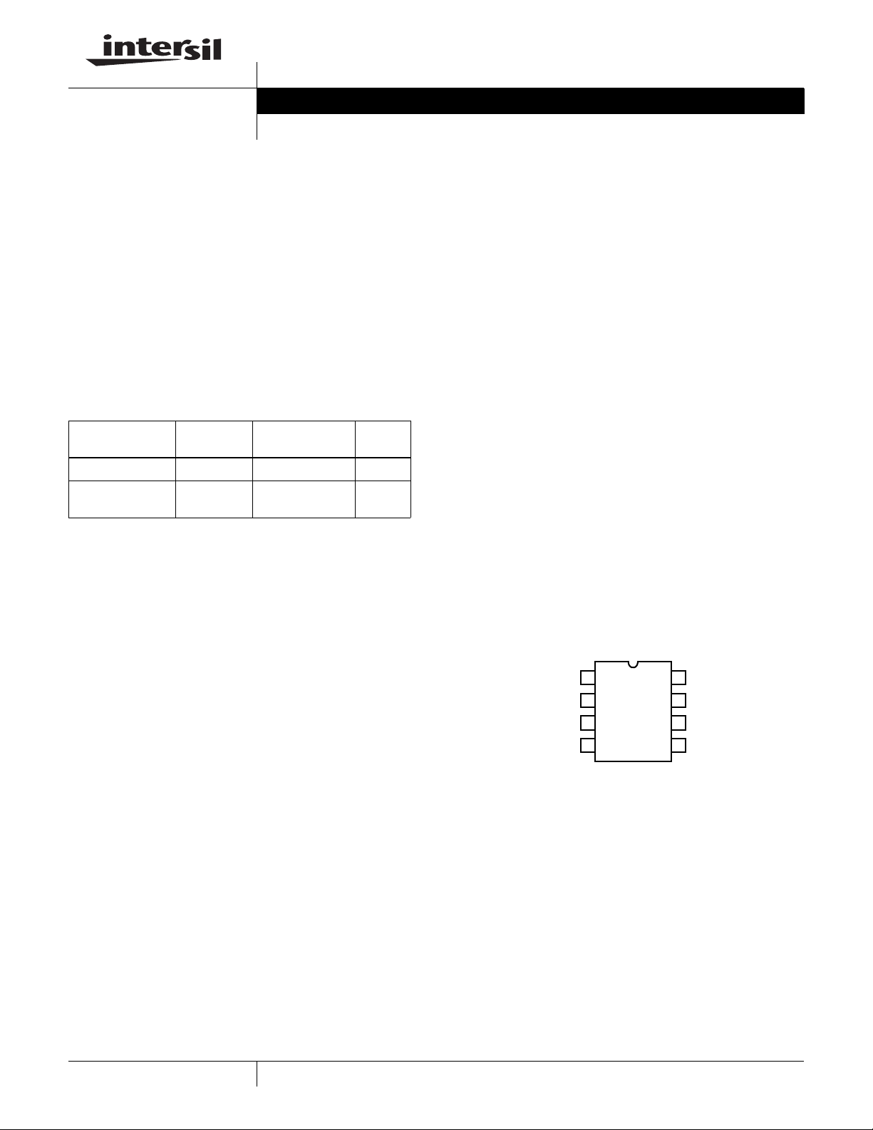
Typical Application Block Diagram
www.BDTIC.com/Intersil
BOOTSTRAP SUPPLY
V
CC
ISL6801
+150VDC MAX
VB
HOH
CONTROLLER
Functional Block Diagram
V
CC
IN
RES
IN
RES
UV
DETECT
&
INPUT LOGIC
ISL6801
&
ON
OFF
LEVEL
SHIFTER
RECHARGE
LEVEL
SHIFTER
DELAY
PATH
HOL
VS
OUTPUT
LOAD
VB
HOH
HOL
GND
VS
Pin Descriptions
PIN NUMBER SYMBOL DESCRIPTION
1V
2 IN Driver Control Signal Input
3 GND Ground
4 RES Driver Enable Signal Input (‘RESET’)
5 VS MOSFET Source Connection
6 HOL MOSFET Gate Low Connection
7 HOH MOSFET Gate High Connection
8 VB Driver Output Stage Supply
NOTE:
The HOL and HOH are the low respective high gate drive output pins. The turn on and turn off time of the external MOSFET could be controlled by
using different resistance values for high and low signal.
CC
2
Driver Supply, Typical 5.0V

ISL6801
www.BDTIC.com/Intersil
Absolute Maximum Ratings Thermal Information
Supply Voltage, VCC . . . . . . . . . . . . . . . . . . . . . . . . . . . . . . . . . .16V
Driver Output Stage Voltage, V
Source Reference Voltage, V
(-5V for 0.5ms, MOSFET Off). . . . . . . . . . . . . . . . . . . . (Min) -1.5V
. . . . . . . . . . . . . . . . . . . . . . . . . . . . . . . . . . . . . . . . . . (Max) 120V
ESD Rating, V
Human Body Model . . . . . . . . . . . . . . . . . . . . . . . . . . . (Min) 820V
(Per MIL-STD-883 Method 3015.7)
ESD
(Referred to GND). . . . . . . . .130V
B
S
Thermal Resistance (Typical, Note 1)
SOIC Package . . . . . . . . . . . . . . . . . . . . . . . . . . . . . 90
Maximum Junction Temperature (Plastic Package) . . . . . . . .150
Maximum Storage Temperature Range . . . . . . . . . -55
Maximum Lead Temperature (Soldering 10s). . . . . . . . . . . . .245
(SOIC Lead Tips Only)
Operating Conditions
Temperature Range. . . . . . . . . . . . . . . . . . . . . . . . . -40oC to 125oC
Supply Voltage Range (Max). . . . . . . . . . . . . . . . . . . . 4.5V to 6.5V
CAUTION: Stresses above those listed in “Absolute Maximum Ratings” may cause permanent damage to the device. This is a stress only rating and operation of the
device at these or any other conditions above those indicated in the operational sections of this specification is not implied.
NOTE:
is measured with the component mounted on a high effective thermal conductivity test board in free air. See Tech Brief TB379 for details.
1. θ
JA
Electrical Specifications All values are over full temperature range.
PARAMETER SYMBOL TEST CONDITIONS MIN TYP MAX UNITS
Operating Temperature Range T
Source Reference Voltage VS -1.8V Continuous, VB/V
Supply Voltage (Note 2) V
Driver Output Supply V
Switching Frequency f Guaranteed by Design 100 - - kHz
Voltage Transconductance (Note 3) dVs/dt - - 500 V/µs
Peak Gate Drive Current I
Continuous Gate Drive Current (Note 3) I
Gate Drive Level LOW V
Gate Drive Level LOW V
Gate Drive Level HIGH V
Gate Drive Level HIGH V
Total IN to Output Delay (Figure 1) td
Total RES to Output Delay (Figure 2) td
Output Rise/Fall Times t
VB Drop Voltage (Figure 4, Note 4) VB
A
CC
VB - VS
V
VB - GND
HOpeak
HOcont
HOL, VS
HOL, VS
VB, HOH
VB, HOH
IN-HOH, L
RES - HOH, L
HOH, L
Fall/Rise
DROP
must stay
OH
low, IN = 0V, RES = 5V, V
6.5V, VB = 5V and 12V,
(Load R = 50Ω, C = 6.8nF)
= -40 to 125oC
T
A
Ident. to VGS of MOSFET Device
Functional
Sink/Source Current VB = 5V and 16V,
100ns
Sink/Source Current Continuous 6.5 8 - mA
IN at H, IHO = 1mA, VB-VS = 5V and 16V - - 0.3 V
IN at H, IHO = 100mA - - 2.2 V
IN at L, IHO = 1mA, VB-VS = 5V and 16V - - 0.5 V
IN at L, IHO = 100mA - - 2.2 V
at VCC = 5.0V, RES = 5V,
Output Trigger Level: 3.5V ON at
VB = 5V, 1.0V OFF at VB = 16V,
Input 2.5V (Load R = 50Ω, C = 6.8nF)
VB-VS = 5V and 16V,
(Load R = 50Ω, C = 6.8nF)
VB-VS = 5V
(Load R = 50Ω, C = 6.8nF)
VB-VS = 16V - 200 500 ns
VB-VS = 9.0V, C
(Load R = 50Ω, C = 6.8nF)
100
= 1µF,
= 4.5V and
CC
-40 - 125
-1.5 - 120 V
4.5 - 6.5 V
4.0 8.5 16.0 V
2.0 - - V
- 200 - mA
-1.03.0µs
-1.03.0µs
- 100 500 ns
- 100 210
(Note 5)
θ
(oC/W)
JA
o
C to 150oC
o
C
mV
o
o
C
C
3

ISL6801
www.BDTIC.com/Intersil
Electrical Specifications All values are over full temperature range. (Continued)
PARAMETER SYMBOL TEST CONDITIONS MIN TYP MAX UNITS
VB Input Current (Note 6) I
VB Input Current I
Driver Supply Current I
Input Threshold LOW (Note 7) IN
Input Threshold HIGH (Note 7) IN
Enable Threshold LOW (Note 7) RES
Enable Threshold HIGH (Note 7) RES
Input Impedance at IN R
Input Impedance at RES R
Logic Input Current at RES (Note 8) I
Undervoltage Shutdown Threshold V
Recharge Resistance (Note 9) R
Recharge Turn On Delay (Note 9) t
Recharge Turn Off Delay t
Recharge Path Voltage Drop Vdrop
NOTES:
2. Shutdown between 3.5V and 4.5V.
3. Parametric limits are guaranteed by design, but not tested in production.
4. The drop voltage is caused by VB to VS current flow during switching. See Figure 3.
5. Assuming 3µs switching overlap, time delay use at testing 100µs.
6. External MOSFET ON or OFF.
7. Input and Enable thresholds tested at V
8. The defined values are to be considered as a maximum allowed value. The input stage does not need to have sink or source capability.
9. The recharge path has to withstand transients in the 120V range for approximately 1µs while injector turn off, causing high power dissipation in
the resistor.
VB
VB
VCC
LOW
HIGH
LOW
HIGH
IN
RES
RES
UV
recharge
RechargeON
RechargeOFF
Recharge
= 4.5V and 6.5V, VB = 12V, VS = 0V, IN at 0V, Response RES at 5.0V.
CC
Static Current, VB-VS = 8.5V,
= 5V, IN = 0V,
V
CC
RES = 5V, (Load R = 50Ω, C = 6.8nF)
Static Current, VB-VS = 8.5V,
= 5V, IN = 0V,
V
CC
RES = 0V, (Load R = 50Ω, C = 6.8nF)
at VCC = 4.5V and 6.5V
(Load R = 50Ω, C = 6.8nF)
VCC = 4.5V and 6.5V 1.4 - - V
VCC = 4.5V and 6.5V - - 3.0 V
VCC = 4.5V and 6.5V 1.4 - - V
VCC = 4.5V and 6.5V - - 3.0 V
at VCC = 5.0V, RES = 5V, IN = 0V,
VB = 12V
at VCC = 5.0V, RES = 5V, IN = 0V,
VB = 12V
at Logic LOW Response HIGH -0.1 - 1.0 mA
VCC to GND, Incl. Hyst. - 3.5 - V
VB = VS = HOH = HOL = 7V, RES = 5V,
IN = 5V, V
at a Constant Current of 1.0mA - - 0.8 V
at a Constant Current of 10mA - - 3.5 V
= 4.5V and 6V
CC
300 750 875 µA
100 550 700 µA
-1.22.5mA
60 100 170 kΩ
60 100 170 kΩ
70 170 350 Ω
71015µs
--1.5µs
4

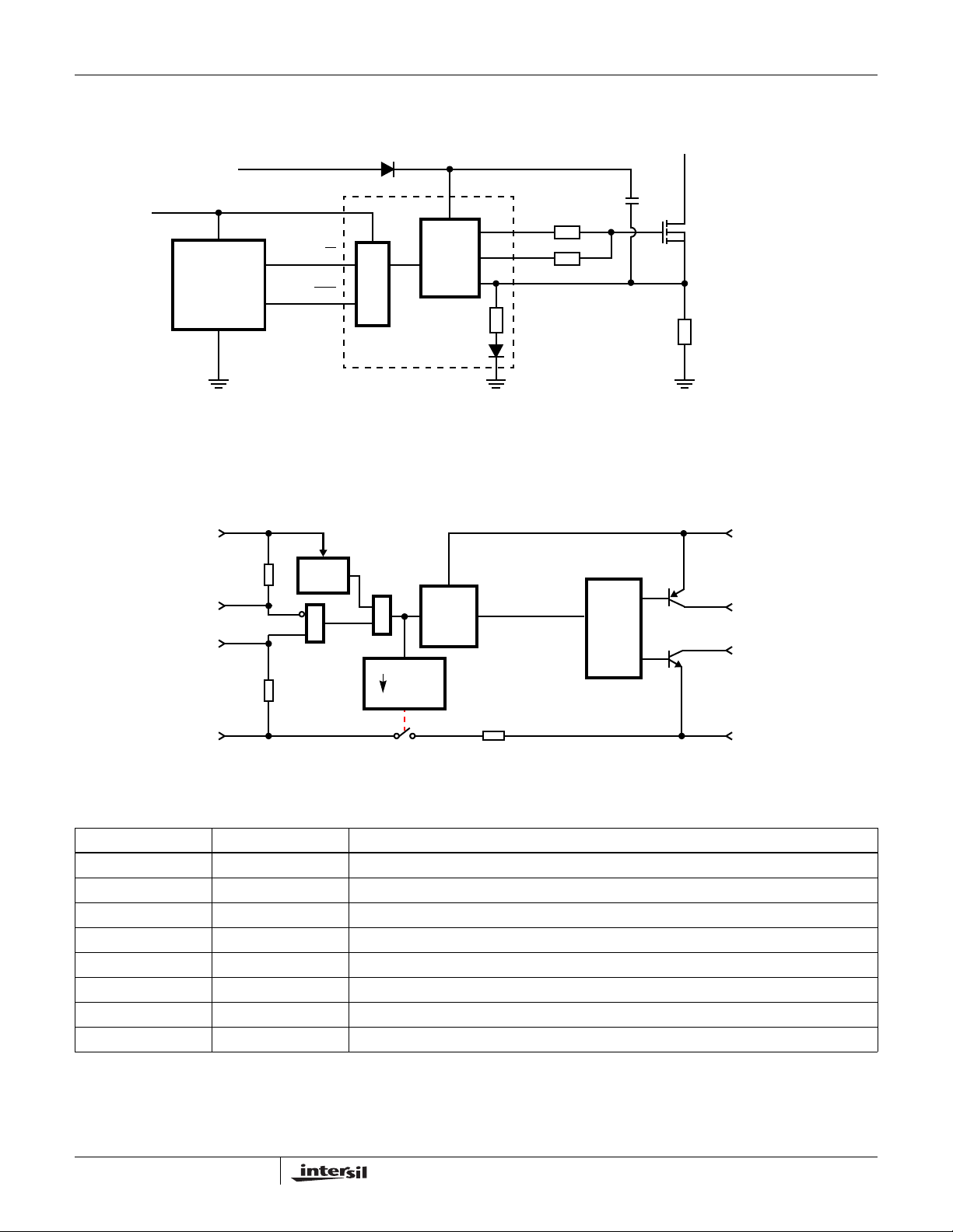
Timing Diagrams
www.BDTIC.com/Intersil
IN
RES
VS
ISL6801
90%
90%
HOH, L
t
RECHARGE
t
RechargeOFF
VB Drop Voltage Test
dIN-HOH, L
t
dIN-HOH, L
ONOFF
t
RechargeON
FIGURE 1. INPUT/OUTPUT TIMING DIAGRAM
IN
RES
HOH, L
td
RES-HOH, L
td
RES-HOH, L
FIGURE 2. RESET TIMING DIAGRAM
10%
t
HOH, Lrise
t
HOH, Lfall
10%
I
g
I
g
1
V
CC
2
IN
IN
3
GND
RES
4
ISL6801
VB
HOH
HOL
VS
8
50R
7
50R
6
5
6n8
1µ
IN
RES
7V
OFF
VB
DROP
BREAK BEFORE MAKEVB-VS
FIGURE 3. VB DROP VOLTAGE TEST CIRCUIT FIGURE 4. VB DROP VOLTAGE DIAGRAM
5
0A

Small Outline Plastic Packages (SOIC)
www.BDTIC.com/Intersil
ISL6801
N
INDEX
AREA
123
-AD
e
B
0.25(0.010) C AM BS
NOTES:
1. Symbols are defined in the “MO Series Symbol List” in Section 2.2 of
Publication Number 95.
2. Dimensioning and tolerancing per ANSI Y14.5M-1982.
3. Dimension “D” does not include mold flash, protrusions or gate burrs.
Mold flash, protrusion and gate burrs shall not exceed 0.15mm (0.006
inch) per side.
4. Dimension “E” does not include interlead flash or protrusions. Interlead flash and protrusions shall not exceed 0.25mm (0.010 inch) per
side.
5. The chamfer on the body is optional. If it is not present, a visual index
feature must be located within the crosshatched area.
6. “L” is the length of terminal for soldering to a substrate.
7. “N” is the number of terminal positions.
8. Terminal numbers are shown for reference only.
9. The lead width “B”, as measured 0.36mm (0.014 inch) or greater
above the seating plane, shall not exceed a maximum value of
0.61mm (0.024 inch).
10. Controlling dimension: MILLIMETER. Converted inch dimensions
are not necessarily exact.
E
-B-
SEATING PLANE
A
-C-
M
0.25(0.010) BM M
H
α
µ
A1
0.10(0.004)
L
h x 45
o
C
M8.15 (JEDEC MS-012-AA ISSUE C)
8 LEAD NARROW BODY SMALL OUTLINE PLASTIC
PACKAGE
INCHES MILLIMETERS
SYMBOL
A 0.0532 0.0688 1.35 1.75 -
A1 0.0040 0.0098 0.10 0.25 -
B 0.013 0.020 0.33 0.51 9
C 0.0075 0.0098 0.19 0.25 D 0.1890 0.1968 4.80 5.00 3
E 0.1497 0.1574 3.80 4.00 4
e 0.050 BSC 1.27 BSC H 0.2284 0.2440 5.80 6.20 h 0.0099 0.0196 0.25 0.50 5
L 0.016 0.050 0.40 1.27 6
N8 87
o
α
0
o
8
o
0
o
8
Rev. 0 12/93
NOTESMIN MAX MIN MAX
-
All Intersil U.S. products are manufactured, assembled and tested utilizing ISO9000 quality systems.
Intersil Corporation’s quality certifications can be viewed at www.intersil.com/design/quality
Intersil products are sold by description only. Intersil Corporation reserves the right to make changes in circuit design, software and/or specifications at any time without
notice. Accordingly, the reader is ca utioned to verify that data she ets are current before pl acing orders. Information fur nished by Intersil is believed to be accurate and
reliable. However, no responsibility is assumed by Intersil or its subsidiaries for its use; nor for any infringements of patents or other rights of third parties which may result
from its use. No license is granted by implication or othe rwise under any patent or patent righ ts of Intersil or its subsidiaries.
For information regarding Intersil Corporation and its products, see www.intersil.com
6
 Loading...