

®
N
www.BDTIC.com/Intersil
数据资料
兼有可调性的同步整流控制及 ZVS 全桥式电流模式
主要特点
April 2005 FN9181.1
ISL6752
PWM 控制器
ISL6752 是高性能, 少引脚的零电压 (ZVS)全桥式脉冲宽度
(PWM)控制器。与 Intersil 的 ISL6551 相似, 通过上层开关启
动于固定的 50%占空比, 下层开关调整脉冲宽度于后沿, 它能
实现ZVS 运行。与熟悉的相位位移控制方法(Phase-Shifted)
比较, 这个方法用较少数目引脚的包装, 相应简单地提供同等
的效率性能以及改善的过流保护和轻载性能。
ISL6752 为同步整流控制具备互补 PWM 输出端。利用外部
控制电压, 这些互补的输出端可以动态地被前置或者延迟。
这个先进的 BiCMOS 设计不但兼容了精确的死区时间控制以
及共振延迟控制, 而且具有一个可调振荡器其频率高达
2MHz。另外, 当跳脉冲可能发生的情况下, 多相脉冲抑制能在
低工作周期时保证相应的输出脉冲。
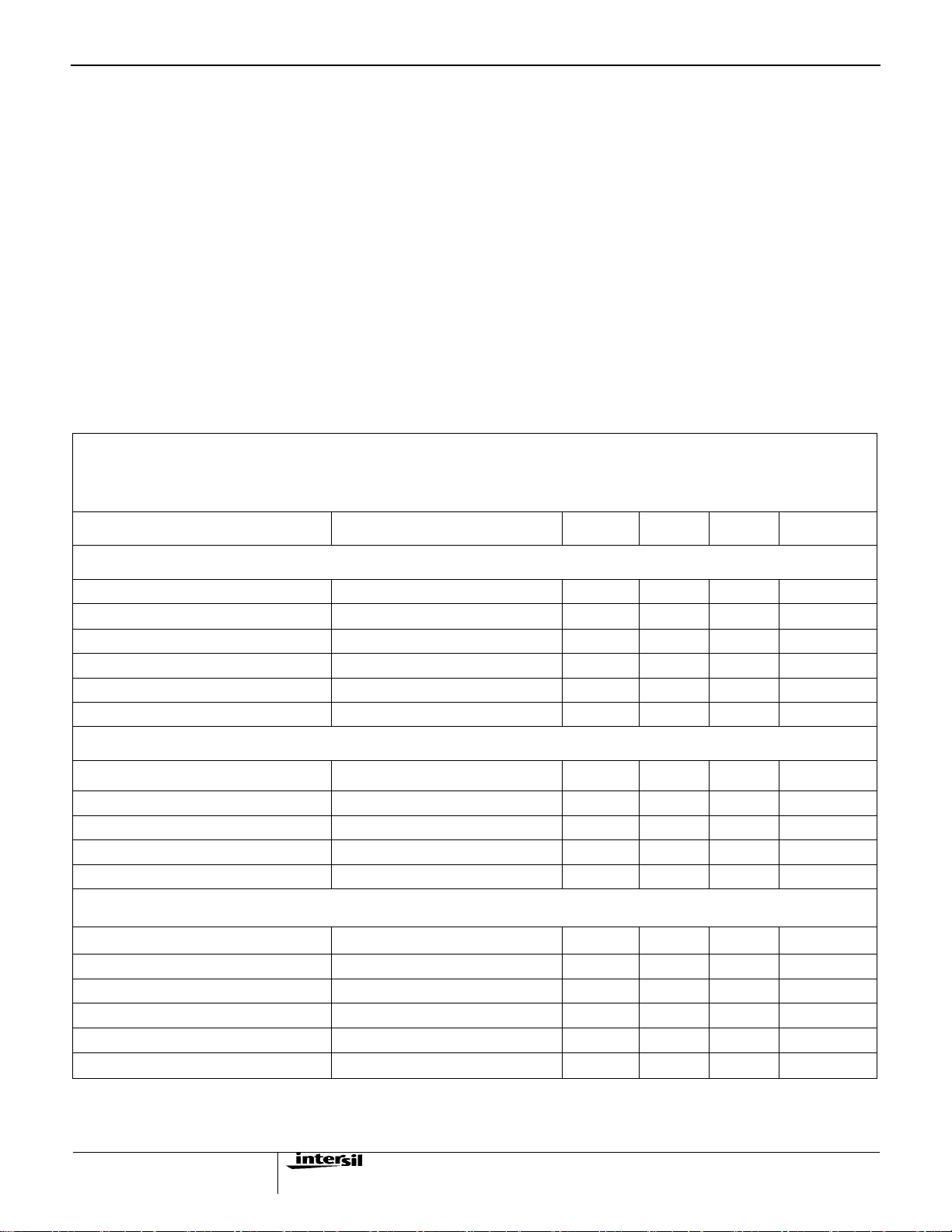
定购资料
零件号码 温度范围
(°C)
ISL6752AAZA
(Note)
Add -T suffix to part number for tape and reel packaging.
NOTE: Intersil Pb-free products employ special Pb-free material
sets; molding compounds/die attach materials and 100% matte tin
plate termination finish, which are RoHS compliant and compatible
with both SnPb and Pb-free soldering operations. Intersil Pb-free
products are MSL classified at Pb-free peak reflow temperatures
that meet or exceed the Pb-free requirements of IPC/JEDEC J
STD-020.
-40 to 105
包装 包装图号 #
16 Ld QSOP
(Pb-free)
M16.15A
• ZVS 运行可调共振延迟
• 延迟/前置可调的同步整流控制输出
• 电流摸式控制
• 3%限流临界
• 可调死区时间控制
• 175µA 启动电流
• 输入电源欠压切断保护
• 可调振荡频率高达 2MHz
• 内部过温保护
• 缓冲振荡锯齿输出
• 快电流传感延迟
• 可调周期性峰值限流电流
• 70ns 上升沿消隐
多脉冲抑制
•
• 不含铅 (RoHS Compliant)
• ELV, WEEE, and RoHS Compliant
应用
• ZVS 全桥转换器
• 电信和信息电源
• 无线基站电源
• 档案服务器电源
• 工业动力系统
插脚引线
ISL6752 (QSOP)
顶视图
1
VADJ
VREF
2
VERR
3
CTBUF
4
RTD
5
RESDEL
6
CT
7
CS
8
16
15
14
13
12
11
10
9
VDD
OUTLL
OUTLR
OUTUL
OUTUR
OUTL LN
OUTLR
GND
1
CAUTION: These devices are sensitive to electrostatic discharge; follow proper IC Handling Procedures.
1-888-INTERSIL or 321-724-7143|Intersil (and design) is a registered trademark of Intersil Americas Inc.
All other trademarks mentioned are the property of their respective owners
Copyright © Intersil Americas Inc. 2005. All Rights Reserved
www.BDTIC.com/Intersil
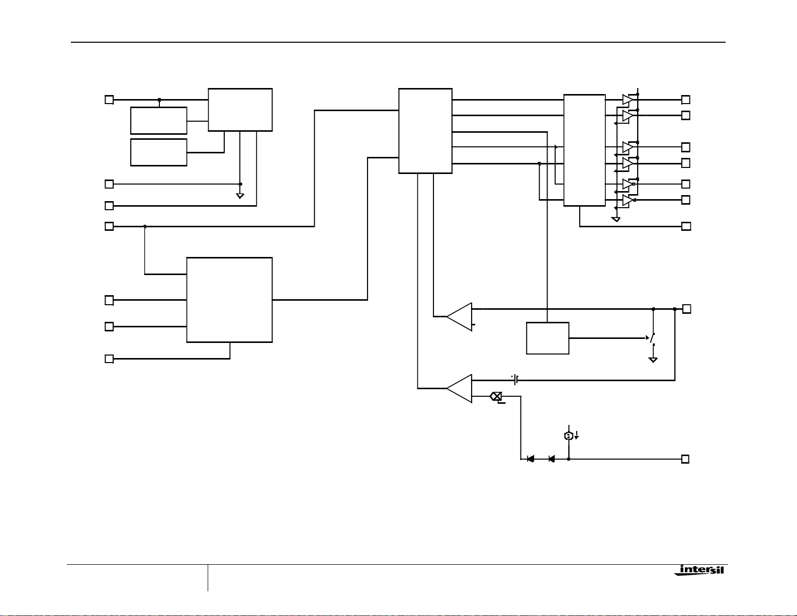
内部电路结构
VDD
TEM PERATUR E
UVLO
OVER-
PROTECTION
VREF
ISL6752
STEERING
LO GIC
PW M
50%
PW M
DELAY/
ADVANCE
TIMING
CONTRO L
VDD
OUTUL
OUTUR
OUTLL
OUTLR
GND
VRE F
RESDEL
CT
RTD
CTBUF
OSCILLATOR
+
-
OVERCURRENT
COMPARATO R
+
-
PWM
COMPARATO R
1.00V
0.33
80m V
70ns
L EADING
EDGE
BLANKING
VREF
1mA
OUTLL N
OUTLRN
VADJ
CS
VERR
2
www.BDTIC.com/Intersil
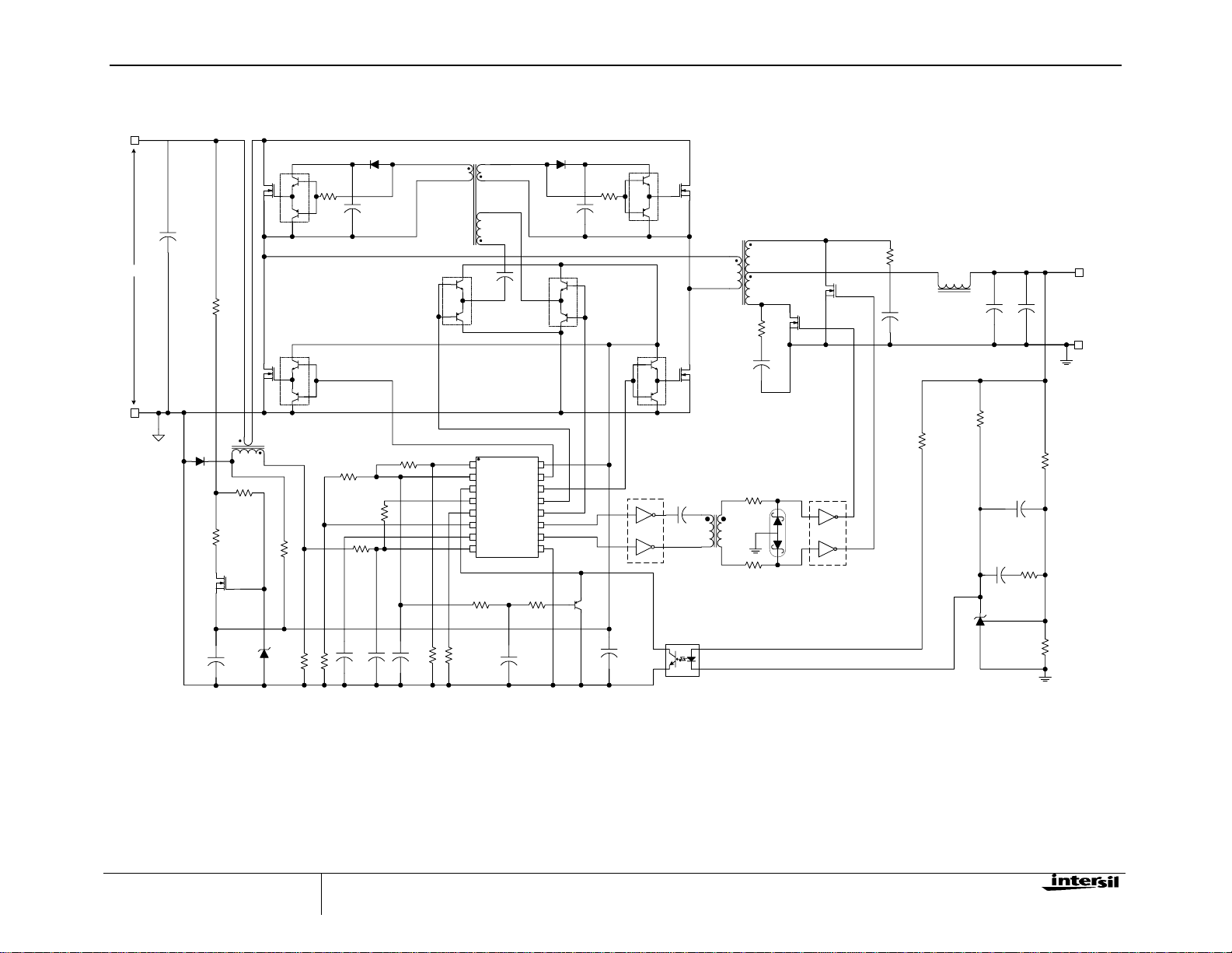
典型应用电路 – 高压输入原边控制 ZVS 全桥转换器
VIN+
VIN-
400 VDC
Q8A
Q8B
Q1
+
C1
R1
Q6A
Q6B
Q4
CR1
T2
R2
R3
R4
Q11
VDD
C2
VR1
R5
R6
CR2
C8
R19
R8
R20
R7
C3
C4
C17
R21
Q10A
Q10B
T3
VADJ VDD
VREF
VERR
CTBUF
RTD
RESDEL
CT
CS GND
R23
R22
C10
ISL6752
OUTLLN
OUTLRN
U1
C16
OUTLL
OUTLR
OUTUL
OUTUR
ISL6752
CR3
Q2
Q5A
R11R10
Q5B
C9
T1
R12
Q9A
Q9B
R13
Q3
Q7A
Q7B
EL7212 EL7212
C5
U5
R24
Q14
U2
C6
C13
R23
T4
CR4
R24
Q12
Q13
U4
C12
L1
C7
C15
R17
U3
+
R18
C14
C11
R15
+ Vout
RETURN
R16
R14
3
www.BDTIC.com/Intersil
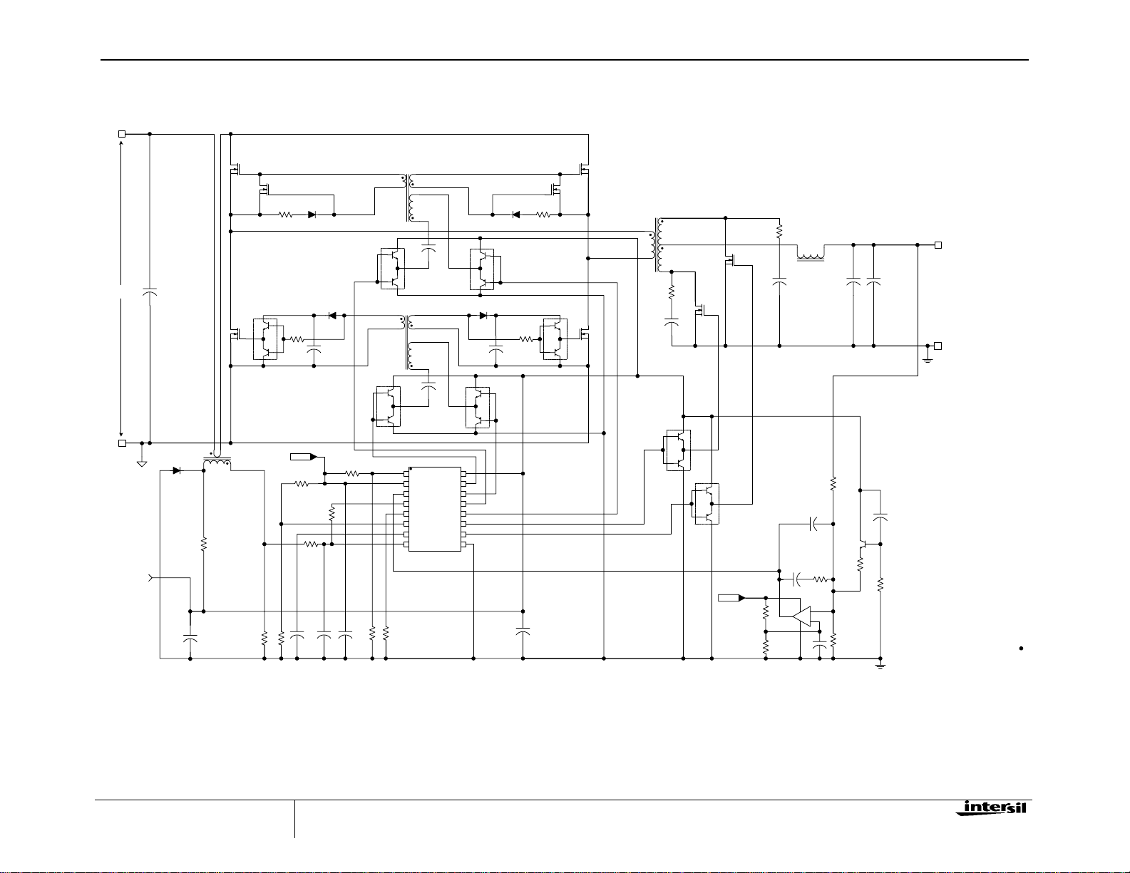
典型应用电路 – 高压输入次边控制 ZVS 全桥转换器
VIN+
ISL6752
VIN-
400 VDC
SECONDARY
BIAS SUPPLY
Q11A
Q11B
Q10A
Q10B
T3
1:1:1
T4
1:1:1
VADJ VDD
VREF
VERR
CTBUF
RTD
RESDEL
CT
CS GND
R5
Q2
Q6
CR3
R12
C10
C7
ISL6752
U1
OUTLL
OUTLR
OUTUL
OUTUR
OUTLLN
OUTLRN
Q12A
Q12B
Q9A
Q9B
CR5
R11
C9
Q3
Q8A
Q8B
C6
T1
Np:Ns:Ns=9:2:2
Np
R14
C11
Ns
Ns
Q13A
Q13B
Q14A
Q14B
R15
Q16
Q15
VREF
R22
R21
L1
C12
C16
C15
R18
U3
-
+
C18
C14
C13
+
R17
C17
Q17
R16
R20
R19
+ Vout
RETURN
Q1
Q5
CR2
R13
+
C1
Q4
Q7A
Q7B
T2
CR1
R1
C2
R2
R3
CR4
R10
C8
VREF
R8
R7
R9
R6
R4
C4
C5C3
4
ISL6752
www.BDTIC.com/Intersil
额定值
Supply Voltage, VDD ----------------GND - 0.3V to +20.0V
OUTxxx ------------------------------------GND - 0.3V to VDD
Signal Pins-------------------------GND - 0.3V to V
REF
+0.3V
Peak GATE Current -----------------------------------------0.1A
ESD Classification
Human Body Model (Per MIL-STD-883 Method 3015.7)------3000V
Charged Device Model (Per EOS/ESD DS5.3, 4/14/93)-------1000V
运行条件
热性能的资料
Thermal Resistance Junction to Ambient (Typical) θJA (oC/W)
16 Lead QSOP (Note 1)-------------------------------------105
Maximum Junction Temperature -------------------55
Maximum Storage Temperature Range-----------65
Maximum Lead Temperature (Soldering 10s)--------------300
o
C to 150oC
o
C to 150oC
o
C
(QSOP – Lead Tips Only)
Supply Voltage Range (Typical)------------------9V-16VDC
Temperature Range
ISL6752AAxx------------------------------ -40
o
C to 105oC
CAUTION: Stress above those listed in “Absolute Maximum Ratings” may cause permanent damage to the device. This is a stress only rating and operation of the
device at these or any other conditions above those indicated in the operational section of this specification is not implied.
Notes:
1) θJA is measured with the component mounted on a low effective thermal conductivity test board in free air. See Tech Brief TB379 for
details.
2) All voltages are with respect to GND.
Electrical Specifications
电气规范
Recommended Operating Conditions, Unless Otherwise Noted. Refer to Block Diagram and Typical Application Schematic.
9V < V
< 20V, RTD = 10.0kΩ, CT = 470pF, TA = -40oC to 105oC (Note 3), Typical values are at TA= 25oC.
DD
PARAMETER TEST CONDITIONS MIN TYP MAX UNITS
SUPPLY VOLTAGE
Supply Voltage - - 20 V
Start-Up Current, IDD V
Operating Current, IDD R
= 5.0V - 175 400
DD
, C
LOAD
=0 - 11.0 15.5 mA
OUT
µA
UVLO START Threshold 8.00 8.75 9.00 V
UVLO STOP Threshold 6.50 7.00 7.50 V
Hysteresis
- 1.75 - V
REFERENCE VOLTAGE
Overall Accuracy
I
VREF
= 0-10mA
4.850 5.000 5.150
V
Long Term Stability TA = 125oC, 1000 hours (Note 4) - 3 - mV
Operational Current (source) -10 - - mA
Operational Current (sink) 5 - - mA
Current Limit VREF = 4.85V -15 - -100 mA
CURRENT SENSE
Current Limit Threshold
VERR = VREF
0.97 1.00 1.03
V
CS to OUT Delay Excl. LEB (Note 4) - 35 50 ns
Leading Edge Blanking (LEB) Duration (Note 4) 50 70 100 ns
CS to OUT Delay + LEB TA = 25oC - - 130 ns
CS Sink Current Device Impedance VCS = 1.1V
Input Bias Current VCS = 0.3V
- - 20
-6.00 - -2.00
Ω
µA
5

ISL6752
www.BDTIC.com/Intersil
Electrical Specifications
电气规范
PARAMETER TEST CONDITIONS MIN TYP MAX UNITS
CS to PWM Comparator Input Offset TA = 25oC 65 80 95 mV
PULSE WIDTH MODULATOR
VERR Pull-Up Current Source VERR = 2.50V 0.80 1.00 1.30 mA
VERR VOH I
Minimum Duty Cycle VERR < 0.6V - - 0 %
Maximum Duty Cycle (per half-cycle)
Zero Duty Cycle VERR Voltage 0.85 - 1.20 V
VERR to PWM Comparator Input Offset TA = 25oC 0.7 0.8 0.9 V
VERR to PWM Comparator Input Gain 0.31 0.33 0.35 V/V
Common Mode (CM) Input Range (Note 4) 0 - 4.45 V
Recommended Operating Conditions, Unless Otherwise Noted. Refer to Block Diagram and Typical Application Schematic.
9V < V
< 20V, RTD = 10.0kΩ, CT = 470pF, TA = -40oC to 105oC (Note 3), Typical values are at TA= 25oC. (continued)
DD
= 0mA 4.20 - - V
LOAD
VERR = 4.20V, VCS = 0V (Note 5) - 94 - %
RTD = 2.00kΩ, CT = 220pF
RTD = 2.00kΩ, CT = 470pF
- 97 - %
- 99 - %
OSCILLATOR
165 183 201 KHz Frequency Accuracy, Overall (Note 4)
-10 - 10 %
Frequency Variation with VDD TA = 25oC, (F
VDD = 10V, |F
– F
|F
0oC
Charge Current TA = 25oC
Discharge Current Gain
105oC
- F
)/F
20V
– F
-40oC
|/F
(Note 4) - 1.5 - %
25oC
- 0.3 1.7 %
10V
10V
|/F
- 4.5 - % Temperature Stability
0oC
0oC
-193 -200 -207
19 20 23
µA
µA/ µA
CT Valley Voltage Static Threshold 0.75 0.80 0.88 V
CT Peak Voltage Static Threshold 2.75 2.80 2.88 V
CT Pk-Pk Voltage Static Value 1.92 2.00 2.05 V
RTD Voltage 1.97 2.00 2.03 V
RESDEL Voltage Range 0 - 2.00 V
CTBUF Gain (V
CTBUFp-p/VCTp-p
) VCT = 0.8V, 2.6V 1.95 2.0 2.05 V/V
CTBUF Offset from GND VCT = 0.8V 0.34 0.40 0.44 V
CTBUF VOH
CTBUF VOL
∆V(I
2.6V
∆V(I
0.8V
LOAD
LOAD
= 0mA, I
= 2mA, I
= -2mA), V
LOAD
= 0mA), V
LOAD
CT
CT
=
=
- - 0.10
- - 0.10
V
V
OUTPUT
High Level Output Voltage (VOH) I
Low Level Output Voltage (VOL) I
Rise Time C
Fall Time C
UVLO Output Voltage Clamp VDD = 7V, I
Output Delay/Advance Range
6
= -10mA, VDD - VOH - 0.5 1.0 V
OUT
= 10mA, VOL - GND - 0.5 1.0 V
OUT
= 220pF, VDD = 15V (Note 4) - 110 200 ns
OUT
= 220pF, VDD = 15V (Note 4) - 90 150 ns
OUT
= 1mA (Note 6) - - 1.25 V
LOAD
= 2.50V (Note 4) - - 3 ns
V
ADJ

电气规范
www.BDTIC.com/Intersil
Recommended Operating Conditions, Unless Otherwise Noted. Refer to Block Diagram and Typical Application Schematic.
OUTLL/OUTLR
Delay/Advance Control Voltage Range
OUTLLN/OUTLRN relative to
OUTLL/OUTLR
V
Delay Time
ADJ
ISL6752
Electrical Specifications
9V < V
< 20V, RTD = 10.0kΩ, CT = 470pF, TA = -40oC to 105oC (Note 3), Typical values are at TA= 25oC.
DD
V
< 2.425V -40 - -300 ns OUTLLN/OUTLRN relative to
ADJ
V
> 2.575V 40 - 300 ns
ADJ
OUTLxN Delayed
OUTLxN Advanced 0 - 2.425 V
TA = 25oC (OUTLx Delayed)
V
= 0V
ADJ
V
= 0.5V 92 105 118 ns
ADJ
V
= 1.0V 61 70 80 ns
ADJ
V
= 1.5V 48 55 65 ns
ADJ
V
= 2.0V 41 50 58 ns
ADJ
TA = 25oC (OUTLx NDelayed)
V
= VREF
ADJ
V
= VREF - 0.5V 86 100 114 ns
ADJ
V
= VREF - 1.0V 59 68 77 ns
ADJ
V
= VREF - 1.5V 47 55 62 ns
ADJ
= VREF - 2.0V 41 48 55 ns
V
ADJ
2.575 - 5.000 V
280 300 320 ns
280 300 320 ns
THERMAL PROTECTION
Thermal Shutdown (Note 4) 130 140 150
Thermal Shutdown, Clear (Note 4) 115 125 135
Hysteresis, Internal Protection (Note 4) - 15 -
NOTES:
3. Specifications at -40
o
C are guaranteed by 25
o
C test with margin limits.
4. Guaranteed by design, not 100% tested in production.
5. This is the maximum duty cycle achieveable using the specified values of RTD and CT. Larger or smaller maximum duty cycles may be
obtained using other values for these components. See Equation 1-3.
6. Adjust VDD below the UVLO stop threshold prior to setting at 7V.
o
C
o
C
o
C
7

0
0
0
www.BDTIC.com/Intersil
典型性能曲线图
1.02
1.01
1
0.99
NORMALIZED VREF
0.98
-40 -25 -10 5 20 35 50 65 80 95 11
ISL6752
25
24
23
22
21
20
19
CT DISCHARGE CURRENT GAIN
18
0 200 400 600 800 100
°
FIGURE
1 REFERENCE VOLTAGE vs. TEMPERATURE FIGURE 2 CT DISCHARGE CURRENT GAIN vs RTD CURRENT
4
1-10
3
1-10
100
DEADTIME TD (ns)
10
0 102030405060708090100
RTD (kΩ)
CT =
10 0 0 pF
68 0 pF
47 0 pF
33 0 pF
22 0 pF
10 0 pF
FIGURE 3 DEADTIME (DT) vs CAPACITANCE FIGURE 4 DEADTIME (DT) vs FREQUENCY
3
1-10
100
F REQ U EN CY ( kH z )
10
0.1 1 1
RTD =
10k
50k
100k
Ω
Ω
Ω
8

www.BDTIC.com/Intersil
各管脚简介
VDD
VDD是控制器的电源输入端。要优化抗扰度, 用一个陶瓷电容
器尽可能靠近并挎接在VDD和GND引脚。
监测VDD是用来做输入电源欠压保护。起动和切断的临限会
密切跟随以保证固定的磁滞。
GND
器件上所有功能和电源地都以这个引脚为基准。由于高峰值
电流以及高频运行, 低阻抗布局是很有必要的。高度推荐使用
接地面以及短线迹。
VREF
这是 5.00V 的基准电压输出端,且有 3%的容差遍及输入、
负载和温度范围。可连接 0.1μF 至 2.2μF 的低 ESR 电容至
GND 以作滤波这输出所需。
CT
振荡器的定时电容可以挎接在这个引脚和GND之间。这个电
容是用200μA 的内部电流源来充电, 其放电是通过用户可以调
整的RTD设置的电流源。
ISL6752
2V会使得共振延迟时间从0%提高到100%的死区时间。把控
制端电压除以2会代表死区时间等于共振延迟。实际上最大共
振延迟必须设置成小于2.0V以保证即使在最大占空比时在上
端FETs开关之前下端FETs处于关断状态。
OUTLL and OUTLR
这两个输出端是用来控制下端FETs, 其脉决宽度被调制并以
交替式运行。OUTLL控制左下FET, OUTLR 控制右下FET。
左边和右边的指示符可以交换只要上端FET输出端, OUTUL
和OUTUR也同时交换。
OUTLLN and OUTLRN
这些输出端与PWM(下端)FETs成互补。OUTLLN与OUTLL成
互补, OUTRN与OUTLR成互补。这些输出端可以用来控制同
步整流器。每个输出端与其互补端的相位关系是由VADJ的电
压值来控制的。
VADJ
这个引脚从0V到5V的控制电压设置OUTLL/OUTLR和
OUTLLN/OUTLRN相对延迟或者前置。不管OUTLL/OUTLR
和OUTLLN/OUTLRN之间的相位调整, OUTUL/OUTUR和
OUTLL/OUTLR的相位关系是不变的。
RTD
这是振荡器的定时电容的放电电流制引脚。跨接在这引脚和
GND的电阻的电流决定CT放电电流的大小。CT放电电流通
常是电阻电流的20倍。这个PWM的死区时间是由定时电容的
放电期间来决定的。在RTD引脚的标称电压是2.00V。
CS
这是过流比较器的输入端。过流比较器的标称临限值设置在
1.00V。PWM输出的任一端被终止会导致CS引脚与GND引脚
短路。
取决于电流取样的内部阻抗,由于内部时钟与外部电源开关
之间的延迟, 可以在输入端串联一个电阻。这个延迟有时会导
致CS引脚在电源开关器件关断之前被放电。
OUTUL and OUTUR
这两个输出端是用来控制上端FETs在固定的50%工作周期以
交替式运行。OUTUL控制左上FET, OUTUR 控制右上FET。
左边和右边的指示符可以交换只要下端FET输出端, OUTLL和
OUTLR也同时交换。
RESDEL
这个引脚是用来设置上端FETs触发与任何一个下端FETs启动
的共振延迟周期。RESDEL引脚上的电压将决定上端FETs何
时开关相对于下端FETs的开关。把控制端电压从0V改变到
9
相对于OUTLL/OUTLR, 电压低于2.425V 会 导 致
OUTLLN/OUTLRN相对前置。相对于OUTLL/OUTLR, 电压高
于2.575V会导致OUTLLN/OUTLRN相对延迟。电压值为2.50
V ±75mV会导致零相位差。如果这个输入端悬浮, 从VREF分
压50%的内部电压会导致无延迟相位。
相位延迟/前置的范围是0或者是40ns与300ns之间, 随着与
2.5V电压差的增加, 相位差也会增大。控制电压与相位差的关
系是非线性的。当控制电压接近2.5V时, 电压增益(∆t/∆V)是很
小的, 并且会随着电压接近控制极限而很快地增大。当选择一
个相当短的延迟/前置时, 这个特点为用户提供不断的准确
性。
VERR
这个输入端为PWM 比较器的倒置输入端提供控制电压。对于
闭环电压调节, 外部误差信号放大器的输出电压可以直接加在
这个输入端, 或者是通过光耦合器。VERR具有额定值为1mA
上拉电流源。
CTBUF
CTBUF是CT引脚上的锯齿振荡波型的缓冲输出以及能够产生
2mA电流。这个引脚的对地偏移电压是0.4V并且谷峰标称增
益为2。这可以用来做斜率补尝。

ISL6752
S
S
S
β
S
www.BDTIC.com/Intersil
功能概述
主要特点
ISL6752最适用于需可调同步整流驱动器且成本低的ZVS全桥
型变换器。ISL6752有许多保护和控制的性能, 需要极少外部
元件。其性能包括: 非常准确的过流保护, 过热保护, 适用于斜
率补偿的隔离锯齿振动器输出, 可调延迟或增加时间的同步整
流器输出, 和可调整的频率。
如果不需要同步整流器, 可应用ISL6753控制器。
振荡器
ISL6752通过改变电阻RTD 和电容CT可调振荡器频率高达
2MH。
开关周期是定时电容充电和放电时间之和。充电时间由CT和
内部200μA电流源决定,而放电时间取决于RTD 和CT
TC11 .5 1 0
T
0.0 6 R TD C T
≈
D
T
SW
3
CT
⋅
⋅≈
⋅⋅()
TCTD+
EQ. 1
+
50 10
⋅
1
---- -- -- --==
F
SW
EQ. 3
9–
EQ. 2
式中: Tc 和 TD分别是充电和放电时间; CT 是定时电容, 其单
位为法拉第 (F); RTD 是放电电阻, 其单位为 欧姆 (Ω); T
振荡器周期; F
是振荡器频率. 一个输出的开关周期等于二
OSC
个振荡器周期。由于每个传输延迟约为10ns,因此实际时间
比所计算的时间稍微长。这个延迟直接增加到开关时间,且
引起定时电容峰值和谷电压门限过冲,因而增大了定时电容
峰-峰的电压。另外,如果使用非常低的充电和放电电流,时
间误差将会因CT引脚处的输入阻抗而增加。流经RTD电流的
最大值应为1mA, 这可产生 20mA 的CT放电电流。
。
是
OSC
1
VREF
2
3
VERR
R
C
4
ISL6752
5
6
7
89
16
15
14
13
12
11
10
FIGURE 5 IMPLEMENTING SOFT-START
图中的 RC 网络决定晶体管基极的上升速度, 而晶体管基极钳
位于 VERR 的电压。 所选的 R 和 C 值应控制 VERR 上升速
度来实现想要的软启动运作时间。软启动运作时间可用等式
6 计算:
---- -- -- -- -- -- -- -- -- -- -- -- -- -- --- -- -- -- -
tRC–1
=
–
ln
⋅
VREF
式中:
V
V
是软启动的钳位电压,
SS
是晶体管基极-发射极的电压跌落,
be
β 是晶体管的平均增益 (DC gain)
如果β足够大, 那项可忽略。肖特基二极管可迅速地放电软启
动电容, 于是电路会迅速复位。
门极驱动器
ISL6752的输出可灌出和吸入10mA电流(在额定的VOH, VOL),
应连接于高电流的MOSFET门极驱动器或分立式的双极推拉
驱动器。 典型的输出电阻是50Ω。
过流运作
V
SSVbe
+
–
0. 00 1R
---- -- -- -- -- -- -- -
EQ. 6
最大占空比(D
MAX
计算:
T
D
DT 1 D–=
C
-----------=
T
SW
EQ. 4
EQ. 5
实现软启动运作
)和死区时间百分比(DT)可用以下公式
当反馈电流信号超过 1.0V, 周期式峰值电流控制可令脉冲式
占空比减少. 当峰值电流超过门限值, 现行的输出脉冲則立即
终止,使负载电流超过门限值时能适当地控制并减低输出电
压。在过流情况下,ISL6752仍可继续运作。
从CS超出电流门限值到输出脉冲终止的传播延迟会因上升沿
封锁(LEB)的间隔而增加。有效延迟是两个延迟之和,其典型
值为105ns。
ISL6752 没有软一启.动运作, 但可用外部元件实现, 如下图所
示。
斜率补偿
峰值电流模式控制需要用斜率补偿来改善噪音干扰,在低负
载时可阻止电流环的不稳定,特别是占空比高于50%时。可
通过加接一外部斜坡到反馈电流信号或在反馈电压误差信号
减接一外部斜坡来实现斜率补偿。加接一外部斜坡到反馈电
流信号是较为常用的方法。
10

ISL6752
V
V
Ω
m
A
V
m
www.BDTIC.com/Intersil
小信号电流模式的模式[1]显示了自然抽样调制器的增益。
Fm,无斜率补偿,是
Fm
1
------------------=
SnTsw
EQ. 7
式中:Sn是锯齿信号的斜率。Tsw是半周时间。若加接一外
部斜坡,调制器的增益则为
Fm
--------------------- -------------Sn Se+
()
1
Tsw
1
--------------------- ----==
m
SnTsw
c
EQ. 8
式中:Se是外部斜坡的斜率以及
mc1
Se
------+=
Sn
EQ. 9
50%的振荡器频率的双极阻尼系数决定外部斜坡的基准额。
若Q系数设置为1,双极会临界阻尼;Q > 1时,过阻尼; Q <
1则会欠阻尼。欠阻尼会引起电流环不稳定。
-----------------------------------------------
Q
=
π
1
m
1D–
()
()
c
0.5–
EQ. 10
式中:D是半周期时间的百分比。设定Q = 1,求得Se为
=
SeS
1
---0.5+
n
π
1
-------------1–
1D–
EQ. 11
Sn和Se分别是电流斜坡和外部斜坡导通时的斜率,与导通时
间(TON) 之积是导通时间(TON) 内所产生的电压变化。
=
VeV
1
---0.5+
n
π
1
-------------1–
1D–
EQ. 12
式中:Vn是导通时间内反馈电流信号的变化,Ve是加外部斜
坡所增加的电压。用输入电压,电流传感器元件和输出电感
可求出V
V
式中:RCS是电流感应电阻,NCT是电流变压器线圈比例,L
n
TSWV
---- -- -- -- ---- -- -- ---- -- -- -- -- ---- -- --
=
e
N
⋅
⋅
O
⋅
CTLO
R
N
CS
1
S
---- ---
--- D 0 . 5–+
⋅
N
π
P
EQ. 13
O
是输出电感,VO是输出电压,而NS和NP分别是副边和原边线
圈。
电感电流通过隔离变压器和电流感应变压器的反射而在感应
电阻上产生的反馈电流信号为
NSR
⋅
V
=
CS
CS
---- -- -- -- -- -- -- ---- -- I
N
⋅
PNCT
DT
⋅
O
SW
--------------------V
+
2L
O
N
IN
S
-------⋅VO–
N
P
EQ. 14
代入等式13和14到等式15,所得的RCS为
NPN
⋅
CT
=
R
CS
---------------------N
---------------------------------------------------
⋅
S
I
O
+
V
O
------- T
L
O
1
1
D
---
SW
----+
2
π
EQ. 16
上述的讨论只用了理想的元件,但在决定外部斜坡所加的数
额时必须考虑磁化电感的影响。磁化电感在反馈电流信号设
了一斜坡补偿幅度并减低外部斜坡的所需值。磁化电感加上
原边电流超出了副边的电感电流。
V
⋅
INDTSW
I
---- -- ---- -- -- ---- -- -- ---- ----=
∆
P
L
EQ. 17
式中:VIN是占空比D的输入电压,Lm是原边磁化电感。电流
感应电阻 (RCS) 的磁化电流效果是
I
∆
⋅
-- -- -- -- ---- -- ---- -- ---=
PRCS
N
CT
EQ. 18
V
∆
CS
若∆VCS大于或等于Ve, 则不需要额外斜坡补偿,而RCS为
N
CS
------------------------------------------------------------------------------------------------------------------------------=
N
S
---- ---I
N
P
DT
+
-- -- -- -- -- -- -- - V
O
2L
SW
O
⋅
R
CT
N
IN
S
-------⋅VO–
N
P
⋅
V
⋅
INDTSW
---- -- -- -- -- -- ---- -- -- ---- -- --+
L
EQ. 19
若∆VCS小于Ve,则仍可用等式16计算RCS值,但含外部斜坡
的斜坡补偿额必须减去∆V
CS。
ISL6752可用CTBUF信号来实现加斜坡补偿。CTBUF是放大
的CT引脚的锯齿信号,偏移接地0.4V,是CT峰-峰振幅的两
倍(0.4 - 4.4V) 。此信号与电流感应反馈的和外加于CS引脚,
如图6所示。
1
2
ISL6752
3
4
CTBUF
5
R9
R6
R
CS
6
7
89
CS
C4
16
15
14
13
12
11
10
式中:VCS是横跨电流感应电阻的电压,IO是输出电流的门限
值。
FIGURE 6 ADDING SLOPE COMPENSATION
由于峰值电流门限值是1.00V,总反馈电流信号和外部斜坡电
压必须加到这个伏数。
假设设计时选择将RC 过滤器放在CS引脚, 加在外部斜坡的
R9 值可叠加得
VeVCS+1=
EQ. 15
11

ISL6752
V
Ω
V
Ω
www.BDTIC.com/Intersil
DV
()
()
V
V
–
∆
e
CS
CTBU F
---- -- ---- -- -- -- -- -- -- -- -- ---- ---- ---- -- -- ---- ---- ---- -- -- ---- ---- ---- ----=
R6 R9+
0.4–
0.4+
R6
⋅
EQ. 20
重新整理,求得R9为
DV
()
()
CTBU F
- --- -- -- -- ---- -- -- ---- ---- -- -- ---- -- -- ---- ---- -- -- ---- -- -- ---- -- -- ---- ---- -- -- ---- -- -- ---- -- -- ---- ---- -- -- --=
R9
0. 4–
V
∆
e
V
–
V
∆
e
CS
0.4++–
V
CS
⋅
R6
EQ. 21
用等式16计得的RCS值必须重新调节, 这样CS引脚的电流感应
信号可由等式14推算出。这主要是由于R6和R9形成分阻器。
R6 R9+
=
′
CS
---------------------R
R9
⋅
CS
EQ. 22
R
例如:
V
= 280V
IN
= 12V
V
O
= 2.0µH
L
O
Np/Ns = 20
Lm = 2mH
= 55A
I
O
振荡器频率, Fsw = 400 kHz
占空比, D = 85.7%
NCT = 50
R6 = 499Ω
用等式16求出电流感应电阻,RCS
R
= 15.1Ω
CS
用等式13确定加在反馈电流信号的电压值,Ve
Ve = 153mV
1
2
VREF
ISL6752
3
4
5
R9
R6
R
CS
FIGURE 7 ADDING SLOPE COMPENSATION USING CT
C4
6
CT
7
CS
89
CT
16
15
14
13
12
11
10
用CT代替CTBUF提供斜坡补偿,除需更改等式20和等式21
外,其余计算一样。等式20改为:
2D R6
V
V
–
∆
e
CS
---------------------=
R6 R9+
⋅
EQ. 23
和等式21改为:
V
2D V
()
R9
---- -- ---- -- -- ---- -- -- ---- ---- -- -- ---- ---- -- -- ---- -- -- ----=
+–
∆
e
–
V
∆
e
R6
⋅
CS
V
CS
EQ. 24
用在CT增设外部斜坡的缓冲晶体管要有足够高的增益(>200)
才可减低所需的基流。但振荡器频率会因所需基流降低流入
CT的充电电流而降低。
接着,用等式18确定磁化电流的效果
= 91mV
∆V
CS
运用等式21求出CTBUF至CS的总和电阻, R9。
R9 = 30.1kΩ
用等式22确定新的R
R’
= 15.4Ω
CS
CS值,R’
CS
上述讨论确定了所需的最小外部斜坡,额外的斜坡补偿可以
用作设计余量。
若应用中需要的死区时间少于约500ns,CTBUF信号不可完
全地作斜坡补偿。CTBUF延迟CT锯齿波300-400ns。这使在
死区时间短而下半周期开始时的CTBUF为非零值。
在这种情况下,斜坡补偿可加额外缓冲的CT信号,如下图所
示。
12
全桥型零电压开关操作
ISL6752 是全桥型零电压开关(ZVS)PWM 控制器。它类似传
统的硬关断拓扑结构控制器, 但非同时启动的对角桥梁开关,
上层开关(OUTUL,OUTUR)启动于固定的 50%占空比,下层
开关(OUTLL, OUTLR) 调整脉冲宽度于后沿。
CT
DEADTIME
OUTLL
OUTLR
OUTUR
OUTUL
FIGURE 8 BRIDGE DRIVE SIGNAL TIMING
PWM
PWM
RESDEL
WINDOW
PWM
RESONANT
DELAY
PWM

ISL6752
L
S
www.BDTIC.com/Intersil
明白 ZVS 方法如何操作,必须包括电路的寄生元素和检测整
个开关周期。
FIGURE 9 IDEALIZED FULL-BRIDGE
图9,半导体开关是以平行二极管和电容的理想的开关元件来
代替,并有理想的输出过滤器和变压器漏感作为隔离元件。
开关电容集总所有寄生电容,其中包括表示电路线组电容。
每个开关有自己特定的位置:左上(UL)、右上(UR)、左下
(LL)、右下(LR)。周期的开始如图10所示,任意地设置在开
关UL和LR开通,在UR和LL关断。原边电流和副边电流分别
P和IS
表示。
以I
通前需多长时间提前拨动。ZVS转换发生在上层开关拨动之
后和对角下层开关开通之前。所需谐振延迟是漏感和寄生电
容所形成的LC电路的谐振频率时间的1/4。 谐振转换可由等
式25推算出
π
---
=
τ
2
式中:τ是谐振转换时间,LL是漏感,CP是寄生电容,R是串
联LL和CP的等效电阻。
通常谐振延迟少于或等于死区时间,并可用下面的等式计
算。
τ
resdel
式中:τ
的0-2V电压,DT是死区时间(见等式1-5) 。
上层开关拨动时,流经UR的原边电流必须找另外的通道。它
充电/放电开关UL和LL的寄生电容直到LL自身二极管偏向前
流。如果RESDEL设置适当,则开关LL会在此时开通。
1
---- -- -- -- -- -- ---- -- -- -- -- ---- -- -1
------------L
LCP
V
---- -- -- -- ---- --- D T
=
resdel
2
R
----------–
2
4L
resdel
⋅
2
是所需的谐振延迟,V
EQ. 25
EQ. 26
是供应到RESDEL引脚
resdel
FIGURE 10 UL - LR POWER TRANSFER CYCLE
由PWM控制的LR开关关断时,UL-LR 能量转换时间就会终
止。但流经原边的电流不能同时中断,故它必须找另外的通
道。原边的电流会流入LR和UR寄生开关电容, 充电到VIN,
然后偏流向上层开关UR的自身二极管。
FIGURE 11 UL - UR FREE-WHEELING PERIOD
原边漏感,LL, 保持电流环流开关UL,原边变压器和开关
UR。当开关LR关掉时,输出电感电流自由运行通过两个输出
二极管,D1和D2。这种情况持续半个周期的余下部份。
CT放电期间,也即死区时间,上层开关拨动。开关UL关断和
开关UR开通,上层开关拨动开关实际时间取决于RESDEL所
设置的谐振延迟。供应到RESDEL的电压决定了下层开关开
FIGURE 12 UPPER SWITCH TOGGLE AND RESONANT
当开关LL关闭时第二次能量转换开始。开关UR和LL开通时的
原边和副边电流流程图如下所示
TRANSITION
FIGURE 13 UR - LL POWER TRANSFER CYCLE
由PWM控制的LR开关关断时,UR-LL 能量转换时间就会终
止。但流经原边的电流不能同时中断,故它必须找另外的通
道。原边的电流流入寄生开关电容, 充电结到VIN,然后偏流
向上层开关UL的自身二极管。原边漏感,L
关UR,原边变压器和开关UL。当开关LL关掉时,输出电感
, 保持电流环流开
L
13

电流自由运行通过两个输出二极管,D1和D2。这种情况持续
www.BDTIC.com/Intersil
半个周期的余下部份。
FIGURE 14 UR - UL FREE-WHEELING PERIOD
ISL6752
上层开关拨动时,流经UR的原边电流必须找另外的通道。它
充电/放电开关UR和LR的寄生电容直到LR自身二极管偏向前
流。如果RESDEL设置适当,则开关LR会在此时开通。
FIGURE 15 UPPER SWITCH TOGGLE AND RESONANT
当开关LR关闭,开始新的周期,第一次能量转换开始。ZVS
转换要求漏感有足够的存储能量令寄生电容充电完全。由于
存储能量与电流平方数成正比(1/2 L
赖于负载。如果漏感没足够存储的能量供给ZVS,可串连一
隔离电感于原边变压器。
TRANSITION
2
) ,ZVS谐振转换是依
LIP
同步整流器输出和控制
ISL6752提供了双端PWM输出,OUTLL和OUTLR,同步整流
器(SR)输出,OUTLLN和OUTLRN。SR输出是PWM输出的
补码。补码输出应连接于PWM输出的反方向,例如,OUTLL
和OUTLRN 是一对,OUTLR 和 OUTLLN是一对。
FIGURE 16 BASIC WAVEFORM TIMING
参见图16,SRs交替同时开通于周期的自由运行期间(OUTLL
/LR关断),和仅有一个开通在OUTLL或OUTLR开通的时
候 。如果OUTLL开通,相应的SR必须是导通的,这表示
OUTLRN是正确的SR控制信号。同样地,如果OUTLR开
通,相应的SR必须是导通的,这表示OUTLLN是正确的SR控
制信号。
ISL6752有一非常有用的性能就是可调PWM输出(OUTLL,
OUTLR) 和它们的补码(OUTLLN, OUTLRN) 相位关系间隔
±300ns。这一性能允许补偿PWM FETs和SR FETs间的传播
时间的差异。而供应到VADJ的电压控制相位关系。
FIGURE 17 WAVEFORM TIMING WITH PWM OUTPUTS
14
DELAYED, 0V < VADJ < 2.425V

ISL6752
www.BDTIC.com/Intersil
+Vdd
ISL6752
VADJ VDD
VREF
VERR
CTBUF
RTD
RESDEL
CT
CS GND
OUTLL
OUTLR
OUTUL
OUTUR
OUTLLN
OUTLRN
ON/OFF
(OPEN = OFF
GND = ON)
FIGURE 18 WAVEFORM TIMING WITH SR OUTPUTS
DELAYED, 2.575V < VADJ < 5.00V
安置VADJ等于VREF/2导致没有任何输出延迟。没有延迟电
压会有±75mV容差窗口。控制电压低于VREF/2零延迟极限会
引起PWM输出OUTLL/LR延迟。控制电压高于VREF/2零延迟
极限则会引起SR输出OUTLLN/LRN延迟。值得注意的是当
PWM输出OUTLL/LR延迟,CS到输出传输延迟会因这延迟的
增加而增加。
通常在一组信号横跨原边-副边隔离范围时PWM和SR输出间
的传输延迟会不相符,而这延迟功能就是用以补偿这不相符
的传输延迟。根据需要可用外电阻,电容和二极管来扩张或
压缩个别的输出脉冲。
50%上层输出会因PWM输出的延迟而同样被延迟,因此是不
会影响谐振延迟设置。
导通/关断控制
ISL6753没有专门的有效/失效的控制引脚。可拉VERR到接地
来令PWM输出和OUTLL/OUTLR失效。这样可降低占空比至
零,但上层50%占空比输出OUTUL/OUTUR会继续运作。同
样地,SR输出OUTLLN/OUTLRN会处于高运作状态。
如果应用中需要所有输出关断,那么供应电压,VDD,必须
分隔于IC。可实现如下图所示。
FIGURE 19 ON/OFF CONTROL USING VDD
故障状况
如果VREF或VDD跌落低于其欠压锁定(UVLO) 门限值或触发
过热保护就会发生故障状况。检测出故障时输出就会截止。
当故障清除后输出重新运作。
过热保护
ISL6752持有内部的过热保护。内热传感器保护器件芯片结温
不超出140˚ C,而热迟滞约15˚ C。
接地要求
为使这个器件能理想地工作,应该要仔细布局。特别是应用
一个好的接地面,VDD和VREF必须以一个好的高频电容直接
旁接到地GND。
参考资料
Ridley, R., “A New Continuous-Time Model for Current
Mode Control”, IEEE Transactions on Power
Electronics, Vol. 6, No. 2, April 1991.
15

ISL6752
www.BDTIC.com/Intersil
Shrink Small Outline Plastic Packages (SSOP)
Quarter Size Outline Plastic Packages (QSOP)
N
IN D EX
AREA
123
-AD
e
B
0.17(0.007) C AMB
E
-B -
SEATING PLANE
A
-C-
S
M
Notes:
1. Symbols are defined in the “MO Series Symbol List” in
Section 2.2 of Publication Number 95.
2. Dimensioning and tolerancing per ANSI Y14.5M-1982.
3. Dimension “D” does not include mold flash, protrusions or
gate burrs and are measured at Datum Plane. Mold flash,
protrusion and gate burrs shall not exceed 0.15mm
(0.006 inch) per side.
4. Dimension “E” does not include interlead flash or
protrusions. Interlead flash and protrusions shall not
exceed 0.25mm (0.010 inch) per side.
5. The chamfer on the body is optional. If it is not present, a
visual index feature must be located within the
crosshatched area.
6. “L” is the length of terminal for soldering to a substrate.
7. “N” is the number of terminal positions.
8. Terminal numbers are shown for reference only.
9. Dimension “B” does not include dambar protrusion.
Allowable dambar protrusion shall be 0.10mm (0.004
inch) total in excess of “B” dimension at maximum
material condition.
10. Controlling dimension: INCHES. Converted millimeter
dimensions are not necessary exact.
0.25(0.010) BM M
H
α
A1
0.10(0.004)
GAUGE
PL A NE
A2
0.25
0.010
L
h x 45°
C
M16.15A
16 LEAD SHRINK SMALL OUTLINE PLASTIC PACKAGE
0.150” WIDE BODY
SYMBOL INCHES MILLIMETERS NOTES
A 0.061 0.068 1.55 1.73 -
A1 0.004 0.0098 0.102 0.249 -
A2 0.055 0.061 1.40 1.55 -
B 0.008 0.012 0.20 0.31 9
C 0.0075 0.0098 0.191 0.249 -
D 0.189 0.196 4.80 4.98 3
E 0.150 0.157 3.81 3.99 4
e 0.025 BSC 0.635 BSC -
H 0.230 0.244 5.84 6.20 -
h 0.010 0.016 0.25 0.41 5
L 0.016 0.035 0.41 0.89 6
N 16 16 7
α
MIN MAX MIN MAX
O
0
8
O
0
O
8
O
-
Rev.2 6/04
All Intersil U.S. products are manufactured, assembled and tested utilizing ISO9000 quality systems.
Intersil Corporation’s quality certifications can be viewed at www.intersil.com/design/quality.
Intersil products are sold by description only. Intersil Corporation reserves the right to make changes in circuit design, software and/or specifications at any time without notice. Accordingly, the
reader is cautioned to verify that data sheets are current before placing orders. Information furnished by Intersil is believed to be accurate and reliable. However, no responsibility is assumed by
Intersil or its subsidiaries for its use; nor for any infringements of patents or other rights of third parties which may result from its use. No license is granted by implication or otherwise under any
patent or patent rights of Intersil or its subsidiaries.
For information regarding Intersil Corporation and its products, see www.intersil.com
16
 Loading...