

Page 1
®
www.BDTIC.com/Intersil
PRELIMINARY
数据资料
精确的死区時間控制的桥型控制器
ISL6745是成本低、双端控制器。主要应用于全桥和半桥型拓
扑结构的电源和线调节的总线变换器。器件的主要特点是精
确的开关频率控制、可调软启动、和过流关断保护。另外,
ISL6745 可精确地调整MOSFET 不交迭的死区時間低至
35ns ,允許电源设计师优化开环总线变换器的效率。
ISL6745 还包括电压控制输入适合于闭环PWM控制和线压前
馈控制。
ISL6745的低启动和运作电流特点,使其在AC-DC和DC-DC
应用容易地偏压。
Data Sheet November 22, 2004 FN9161.3
主要特点
• 精确的占空比和死区時間控制
• 100µA 启动电流
• 可调延迟过流关断和重新启动
• 可调振荡器频率高至 2MHz
• 1A MOSFET 门极驱动器
• 可调软启动
• 内部过热保护
• 控制到输出的延迟是 35ns
• 体积小和极少的外部元件
• 输入欠压保护
• 不含 Pb 的包装
ISL6745
这先进的BiCMOS设计特点是可调开关频率高至1MHz,1A
FET驱动器,和非常低的传输延迟适合于过流快反应。
定购资料
零件号码 温度范围
ISL6745AU -40 to 105 10 Ld MSOP M10.118
ISL6745AUZ
(See Note)
Add -T suffix to part number for tape and reel packaging
NOTE: Intersil Pb-free products employ special Pb-free material sets;
molding compounds/die attach materials and 100% matte tin plate
termination finish, which are RoHS compliant and compatible with both SnPb
and Pb-free soldering operations. Intersil Pb-free products are MSL classified
at Pb-free peak reflow temperatures that meet or exceed the Pb-free
requirements of IPC/JEDEC J STD-020C.
(°C) 包装 包装图号 #
-40 to 105
10 Ld MSOP
(Pb-free)
M10.118
应用
• 半桥和全桥型拓扑结构的变换器
• 线调节的总线变换器
• AC-DC 电源
• 通信、信息和档案服务器的电源
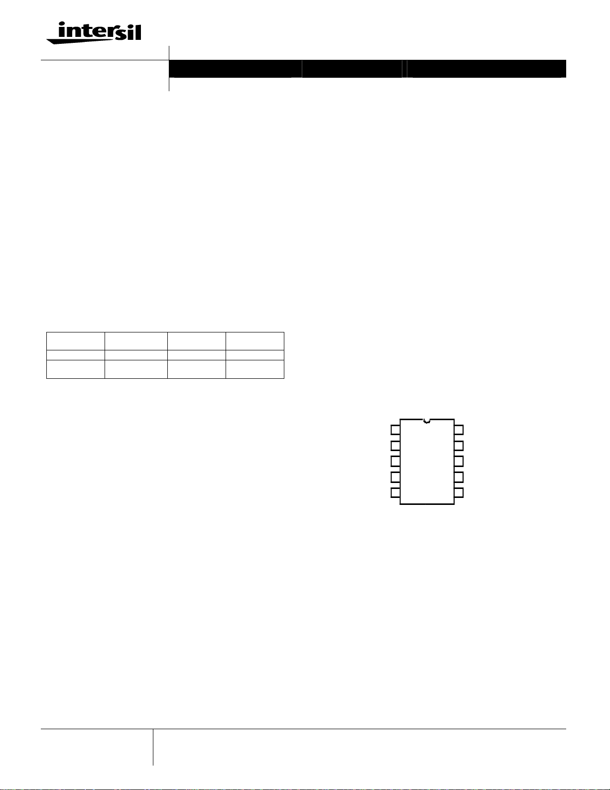
插脚引线 (顶视图)
ISL6745 (MSOP)
SS 1
RTD
2
3
VE RR
4
CS
5
CT
10
9
8
7
6
VDD
VDDP
OU TB
OU TA
GN D
1
CAUTION: These devices are sensitive to electrostatic discharge; follow proper IC Handling Procedures.
1-888-INTERSIL or 321-724-7143|Intersil (and design) is a registered trademark of Intersil Americas Inc.
All other trademarks mentioned are the property of their respective owners
Copyright © Intersil Americas Inc. 2004. All Rights Reserved
Page 2

V
www.BDTIC.com/Intersil
GND
ISL6745
V
FL
V
V
DD
UVLO
+
-
INTERNAL
BG
OT SHUTDOWN
130 - 150 C
BIAS
5.00 V
BIAS
Q
T
Q
PWM TOGGLE
DDP
OUTA
OUTB
V
BIAS
70 uA
ON
V
BIAS
SS CLAMP
R
TD
I
RTD
V
BIAS
160 uA
ON
C
T
RTD
= 55 x I
DCH
I
CS
2.0 V
-
15 uA
PEAK
+
-
VALLEY
+
0.6 V
PWM COMPARATOR
C
T
+
-
-
SRQ
Q
RESET
DOMINANT
+
-
CLK
OC DETECT
2.8 V
0.8 V
I
DCH
ON
V
BIAS
-
+
4.0 V
50 µS
RETRIGGERABLE
ONE SHOT
SRQ
Q
PWM LATCH
SET
DOMINANT
+
SS CHARGED
-
SRQ
Q
OC LATCH
Q
Q
V
UV
BIAS
4.65V ↓ 4.80V ↑
+
-
3.9 V
SS LOW
FAULT LATCH
SET DOMINANT
SRQ
FL
Q
-
+
BG
+
SS
15 uA
0.27 V
-
SS
V
BIAS
V
ERR
0.8
SS
0.8
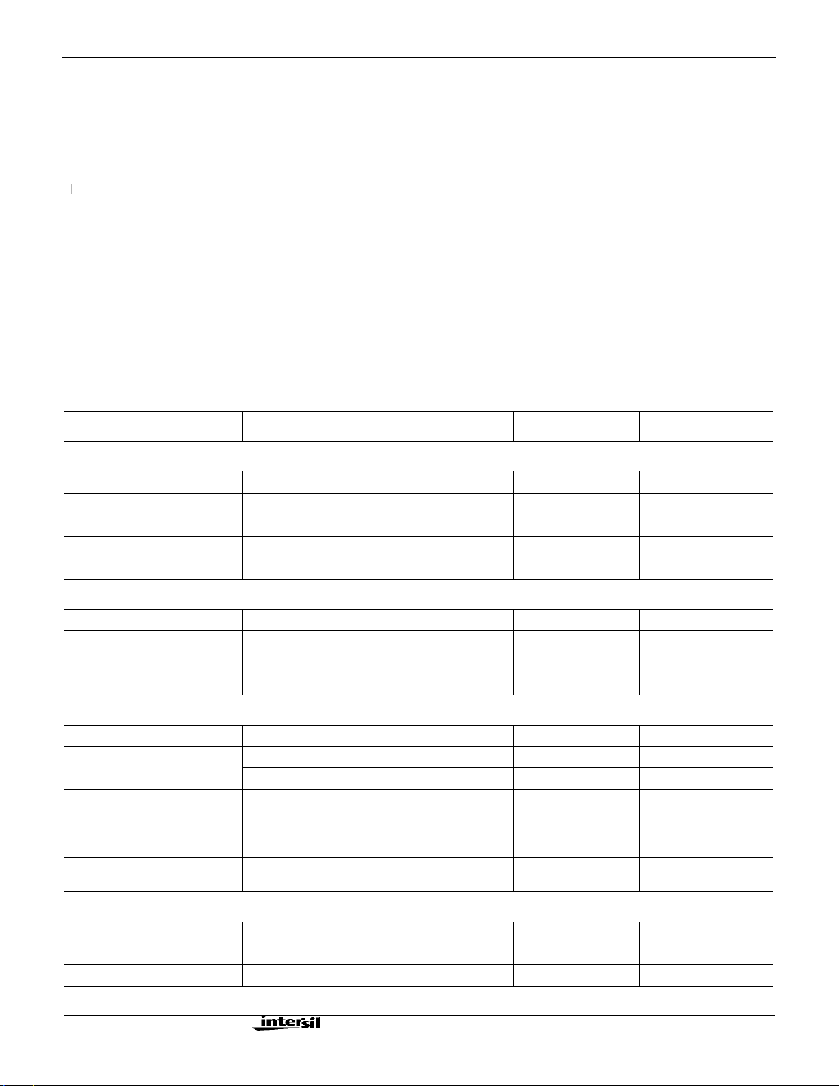
ISL6745 内部电路结构
2
Page 3
ISL6745
电气规
范
www.BDTIC.com/Intersil
额定值 热性能的资料
bsolute Voltage Ratings
Supply Voltage, VDD----------------------GND-0.3V to +20V
OUTA, OUTB ------------------------------- GND -0.3V to V
Signal Pins------------------------------------- GND-0.3V to 5V
Peak GATE Current ------------------------------------------- 1A
ESD Classification
Human Body Model (Per JEDEC22 std. Method A114-B)---Class 2
Machine Model (Per JEDEC22 std. Method A115-A)---------Class A
Recommended Operating Conditions
运行条件
Supply Voltage Range (Typical) -------------------9-16VDC
Temperature Range
ISL6745AU--------------------------------- -40
CAUTION: Stress above those listed in “Absolute Maximum Ratings” may cause permanent damage to the device. This is a stress only rating and operation of the
device at these or any other conditions above those indicated in the operational section of this specification is not implied.
NOTES:
1) θJA is measured with the component mounted on a low effective thermal conductivity test board in free air. See Tech Brief TB379 for
details.
2) All voltages are to be measured with respect to GND, unless otherwise specified.
o
C to 105oC
DD
Thermal Information
Thermal Resistance (Typical, Note 1) ---------- θJA (oC/W)
10 Lead MSOP ------------------------------------------------ 128
Maximum Junction Temperature ---------- -55
Maximum Storage Temperature Range - -65
Maximum Lead Temperature (Soldering 10s)------ 300
o
C to 150oC
o
C to 150oC
o
C
Electrical Specifications
Recommended Operating Conditions, Unless Otherwise Noted. Refer to Block Diagram and Typical Application Schematic.
PARAMETER TEST CONDITIONS MIN TYP MAX UNITS
SUPPLY VOLTAGE
9V<V
<16V, RTD= 51.1KΩ, CT = 470pF, TA = -40oC to 105oC (Note 4), Typical values are at TA= 25oC.
DD
Start-Up Current, IDD V
Operating Current, IDD C
UVLO START Threshold 5.9 6.3 6.6 V
UVLO STOP Threshold
Hysteresis
CURRENT SENSE
Current Limit Threshold
CS to OUT Delay
CS Sink Current
Input Bias Current
PULSE WIDTH MODULATOR
Minimum Duty Cycle
Maximum Duty Cycle
V
to PWM Comparator Input
ERR
Gain
CT to PWM Comparator Input
Gain
SS to PWM Comparator Input
Gain
< START Threshold - - 175
DD
= 1nF - 5 8.5 mA
OUTA, B
(Note 4)
V
R < CT Offset
ERRO
CT = 470pF, RTD = 51.1KΩ
C
= 470pF, RTD = 1.1KΩ (Note 4)
T
(Note 4)
(Note 4)
5.3 5.7 6.3
- 0.6 -
0.55 0.6 0.65
- 35 -
8 10 -
-1 - 1
- - 0
- 94 -
- 99 -
- 0.8 -
- 1 -
- 0.8 -
µA
ns
mA
µA
V/V
V/V
V/V
V
V
V
%
%
%
OSCILLATOR
T
= 25oC
Charge Current
RTD Voltage
Discharge Current Gain
A
143 156 170
1.925 2 2.075
45 - 65
3
µA
V
µA/µA
Page 4

ISL6745
电气规
范
www.BDTIC.com/Intersil
Recommended Operating Conditions, Unless Otherwise Noted. Refer to Block Diagram and Typical Application Schematic.
PARAMETER TEST CONDITIONS MIN TYP MAX UNITS
<16V, RTD= 51.1KΩ, CT = 470pF, TA = -40oC to 105oC (Note 4), Typical values are at TA= 25oC. (Continued)
9V<V
DD
Electrical Specifications
CT Valley Voltage
CT Peak Voltage
SOFT-START
Net Charging Current
SS Clamp Voltage
Overcurrent Shutdown Threshold
Voltage
Overcurrent Discharge Current
Reset Threshold Voltage (Note 4)
OUTPUT
High Level Output Voltage (VOH) VDD – V
Low Level Output Voltage (VOL) I
Rise Time C
Fall Time C
THERMAL PROTECTION
Thermal Shutdown (Note 4)
Thermal Shutdown Clear (Note 4)
Hysteresis, Internal Protection (Note 4)
NOTES:
o
3. Specifications at -40
4. Guaranteed by design, not 100% tested in production.
C are guaranteed by design, not production tested.
(Note 4)
OUTA
I
= -100mA
OUT
= 100mA
OUT
= 1nF, VDD = 12V
GATE
= 1nF, VDD = 12V
GATE
or V
OUTB
0.75 0.8 0.85 V
2.70 2.80 2.90 V
45 - 68
3.8 4.0 4.2 V
- 3.9 - V
12 15 23
0.25 0.27 0.30 V
,
- 0.5 2.0 V
- 0.5 1.0 V
- 17 60 ns
- 20 60 ns
- 145 -
- 130 -
- 15 -
µA
µA
o
C
o
C
o
C
4
Page 5

www.BDTIC.com/Intersil
典型性能曲线图
ISL6745
5
Page 6

ISL6745
www.BDTIC.com/Intersil
ISL6745各管脚简介
V
DD
VDD为电源输入端。要优化抗扰度,用一个陶瓷电容器尽可
能靠近并挎接在VDD和GND引脚。
IC总供应电流,IDD,取决于OUTA和OUTB输出端的负载。
电流是 静态电流和平均输出电流的总和。平均输出电流
I
DD
(I
)与操工作频率(FSW)和每输出端的负载电容的电荷量(Q)
OUT
成正比,其值可用下式 计 算:
SWOUT FQ2I ××= (EQ. 1)
R
TD
这是振荡器定时电容放电电流控制引脚。一个电阻器应连接
在这引脚和GND之间。而流经这个电阻的电流决定放电电流
的大小。放电电流的通常值则是这电流的55倍。PWM死区时
间由定时电容放电时间决定。
C
T
振荡器定时电容应连接在这引脚和GND之 间。
CS
这是过流保护比较器的输入端。过流比较器门限值设置为典
型值0.600V。在每个开关周期的末端,CS引脚短接于GND。
根据电流传感源阻抗,由于内部时钟和外部电力开关间的延
迟,可能要求串联一个电阻。
超出过流门限值会启动延迟关断程序。一旦检测出过流情
况,软启动充电电流源就会被截止。而软启动电容通过15µA
电流源放电,如果软启动电压降至于3.9V(可承受的过流门限
OUTA and OUTB
OUTA 和 OUTB 为交替半周期输出端。每个输出具有 1A 峰
值电流的输出能力可驱动 MOSFETs 或 MOSFET 驱动器,且
以非常低的阻抗降低过冲和下冲。
SS
在这个引脚与 GND 之间连接软启动定时电容器来控制软启动
的时间。电容值决定启动时占空比的增长率,且控制过流关
断延迟和过流与短路间歇再启动周期。
功能概述
主要特点
ISL6745 为那些以低成本的桥型拓扑结构且要求准确频率和
死区时间控制的应用提供了一个极佳的选择。它有很多特
点,其中有 1AFET 驱动器、可调软启动、过流保护和内部过
热保护,因而 ISL6745 能以最少量的外部元件做出一个高度
灵活的设计。
振荡器
ISL6745通过改变电阻R
Hz。开关周期是定时电容充电和放电时间之和。充电时间由
CT和内部电流源(在式中采用160µA)决定,而放电时间取决于
R
和C
TD
T。
C C1025.1T •×≈
4
T ••≈
和电容CT来调振荡器频率高达2M
TD
s (EQ.2)
T
1
ineCurrentGaargCTDisch
TTDD CR
s (EQ. 3)
值) 关断条件出现,OUTA和OUTB输出会强制降低。当软启
动电压降至0.27V(重新设置门限值) ,一个新软启动周期开
始。
如果过流情况中断,且在50µs时间内未达到关断门限值
(3.9V),过流关断是不会发生。软启动充电电流重新运行
且软启动电压复位。
GND
T
分别是大概的充电和放电时间,T
C和TD
行周期,而F
(DischargeCurrentGain=45 to 65)可在第3页的表(或Figure1)
找到。一个输出的开关周期等于二个振荡器周期。由于传输
延迟约5ns,实际 时间比所计算的时间稍微长。这个延迟直
接增加到开关时间,且引起定时电容峰值和谷电压门限过
器件上所有功能和电源地都以这个引脚为基准。由于高峰值
冲,因而增大了定时电容峰-峰的电压。另外,如果使用非常
电流和高频工作,布局必须是低阻抗的。故建议使用地线板
低充电和 放电电流, 时间误差将会因C
块和短接线。
增加。
6
TTT =+=
1
DCOSC
OSC
s (EQ. 4)
OSC
F
是振荡器自由运
OSC
是振荡器频率。放电电流增益
引脚处的输入阻抗而
T
Page 7

ISL6745
www.BDTIC.com/Intersil
EQ.2至4可帮助估计振荡器频率。在实际上,寄生电部的C
电容,RTD电压的变化和充电电流遍及温度的变化及其他变化
是不可被忽视的。这些对频率的影响最好在真的电路板里评
价。EQ. 2依据于基本的电容电流公式,I=C*dV/dt。根据R
电压的变化(如图4)和充电电流变化(如图5),公式2的结果将
会不同计算出的结果。典型性能曲线和上述的公式一起更精
确地估计工作频率。
最大占空比(D
C
MAX
T
OSCT
D =
)和死区时间(DT)可用以下公式计算:
MAX
OSC
T
MAX
)D1(TD
−×= (EQ. 6)
TD
(EQ. 5)
软启动运作
ISL6745使用外部电容和内部电流电源来作软启动。软启动降
低启动期间的电压和浪涌电流。
在用以驱动 PWM 门控的软启动比较器里,振荡器电容 C
号与软启动 SS 电压作比较。当软启动电压(SS)少于 2.8V
信
T
T
过热保护
内热传感器保护器件芯片结温不超出145˚C,而热迟滞约15˚
C。
时,占空比会受到限制。输出脉宽随着软启动电容电压的增
加而增加。这使软启动期间的占空比可从零增加到最大脉
宽。当软启动电压超过 2.8V,软启动完成。软启动开始于起
动或因过流关断而复位时。 软启动电压被钳位在 4V.
门极驱动器
ISL6745可灌出和吸收1A峰值电流,且可连接一个MOSFET
驱动器如ISL6700作电平转移之用。如要限制峰值电流通过
IC,一个外部电阻应连接在IC的推拉输出(OUTA或OUTB引
脚)和 MOSFET的门极之间。而这个小串联电阻能阻尼由线组
寄生 电感和FET的输入电容的共振所产生的振荡。
过流运作
软启动周期完成后,过流延迟关断保护才启动。如果检测出
过流情况,软启动充电电流电源就会中止,且软启动电容通
过15µA电源放电。过流情况停止后,在50µs时间内,如果软
启动电容器放电至3.9V,输出停止。这种状态持续到软启动
电压降至270mV,开始新软启动周期。如果在软启动电压降
至的3.9V前,且过流情况停止至少50µs,软启动充电电流会
恢复正常运作,而软启动电压会复位。
7
Page 8

ISL6745
www.BDTIC.com/Intersil
Mini Small Outline Plastic Packages (MSOP)
M10.118 (JEDEC MO-187BA)
10 LEAD SHRINK NARROW BODY SMALL OUTLINE
EE1
PLASTIC PACKAGE
INDEX
AREA
AA1A2
-H-
SID E V IEW
12
TOP VIEW
b
e
D
-B-
0.20 (0.008) A BC
0.25
GAUG E
PL AN E
SE AT IN G
PLANE
0.10 (0.004) C
-A-
0.20 (0.008) C
(0.01 0)
-C-
0.20 (0.008) C D
SEATING
PLANE
a
4X
θ
θ
4X
L1
C
L
E
1
END VIEW
R1
L
C
-B-
NOTES:
1. These package dimensions are within allowable
dimensions of JEDEC MO-187BA.
2. Dimensioning and tolerancing per ANSI Y14.5M-1994.
3. Dimension “D” does not include mold flash, protrusions or
gate burrs and are measured at Datum Plane. Mold flash,
protrusion and gate burrs shall not exceed 0.15mm
(0.006 inch) per side.
4. Dimension “E1” does not include interlead flash or
protrusions and are measured at Datum Plane. Interlead
flash and protrusions shall not exceed 0.15mm (0.006
inch) per side.
5. Formed leads shall be planar with respect to one another
within 0.10mm (.004) at seating Plane.
6. “L” is the length of terminal for soldering to a substrate.
7. “N” is the number of terminal positions.
8. Terminal numbers are shown for reference only.
9. Dimension “b” does not include dambar protrusion.
Allowable dambar protrusion shall be 0.08mm (0.003 inch)
total in excess of “b” dimension at maximum material
condition. Minimum space between protrusion and
adjacent lead is 0.07mm (0.0027 inch).
10. Datums -A- and -B-to be determined at Datum plane -H- .
11. Controlling dimension: MILLIMETER. Converted inch
dimensions are for reference only
SYMBOL INCHES MILLIMETERS NOTES
MIN MAX MIN MAX
A 0.037 0.043 0.94 1.10 -
A1 0.002 0.006 0.05 0.15 -
A2 0.030 0.037 0.75 0.95 -
b 0.007 0.011 0.18 0.27 9
c 0.004 0.008 0.09 0.20 -
D 0.116 0.120 2.95 3.05 3
E1 0.116 0.120 2.95 3.05 4
e 0.020 BSC 0.50 BSC -
E 0.187 0.199 4.75 5.05 -
L 0.016 0.028 0.40 0.70 6
L1 0.037 REF 0.95 REF -
N 10 10 7
R 0.003 - 0.07 - -
R1 0.003 - 0.07 - -
θ
α
o
15o 5
5
o
6
0
o
0
o
15o
o
6
o
-
Rev.0 12/02
All Intersil U.S. products are manufactured, assembled and tested utilizing ISO9000 quality systems.
Intersil Corporation’s quality certifications can be viewed at www.intersil.com/design/quality.
Intersil products are sold by description only. Intersil Corporation reserves the right to make changes in circuit design, software and/or specifications at any time without notice. Accordingly, the
reader is cautioned to verify that data sheets are current before placing orders. Information furnished by Intersil is believed to be accurate and reliable. However, no responsibility is assumed by
Intersil or its subsidiaries for its use; nor for any infringements of patents or other rights of third parties which may result from its use. No license is granted by implication or otherwise under any
patent or patent rights of Intersil or its subsidiaries.
For information regarding Intersil Corporation and its products, see www.intersil.com
8
 Loading...