

Page 1
®
數据資料
先進的雙端 PWM 控制器
主要特點
July 2005 FN9183.0
ISL6742
ISL6742是高性能雙端(PWM)控制器并具備先進的同步整流
控制以及限流臨界的特點。它能用于電流以及電壓模式控制
方法。
ISL6742為同步整流控制具備互補PWM輸出端。利用外部控
制電壓, 這些互補的輸出端可以動態地被前置或者延遲。
它的优秀的電流傳感電路使用取樣及保存的方法提供精确的
平均電流信號。适用于平均限流保護, 這种保護方法消除了峰
值限流方法的局限, 也适用于均流電路以及平均電流模式控
制。
這個先進的BiCMOS設計不但兼容了一個可調振蕩器其頻率
高達2MHz, 內部過溫保護, 精确的死區時間控制以及共振延遲
控制。另外, 當跳脈沖可能發生的情況下, 多相脈沖抑制能在
低工作周期時保證相應的輸出脈沖。
定購資料
零件號碼 溫度范圍
(°C)
ISL6742AAZA
(Note)
Add -T suffix to part number for tape and reel packaging.
NOTE: Intersil Pb-free products employ special Pb-free material
sets; molding compounds/die attach materials and 100% matte tin
plate termination finish, which are RoHS compliant and compatible
with both SnPb and Pb-free soldering operations. Intersil Pb-free
products are MSL classified at Pb-free peak reflow temperatures
that meet or exceed the Pb-free requirements of IPC/JEDEC J
STD-020.
-40 to 105
包裝 包装圖號 #
16 Ld QSOP
(Pb-free)
M16.15A
• 延遲/前置可調的同步整流控制輸出
• 可調平均電流信號
• 3%峰值限流臨界
• 快電流傳感延遲
• 可調振蕩頻率高達 2MHz
• 可調死區時間控制
• 電壓或電流模式控制
• RAMP 以及 CS 分開輸入益于電壓前饋控制或者電
流模式控制
• 誤差放大器的參考電壓具備精确的容差遍及輸入、
負載和溫度范圍
• 175µA 啟動電流
• 輸入電源欠壓切斷保護
• 可調軟啟動
70ns 上升沿消隱
•
• 多脈沖抑制
• 內部過溫保護
• 不含鉛, 以及 ELV, WEEE, and RoHS Compliant
應用
• 半橋, 全橋, 正向交錯, 以及推挽轉換器
• 電信和信息電源
• 無線基站電源
• 檔案服務器電源
• 工業動力系統
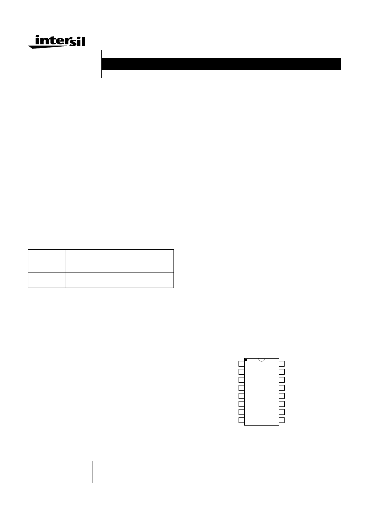
插腳引線
ISL6742 (QSOP)
頂視圖
1
CAUTION: These devices are sensitive to electrostatic discharge; follow proper IC Handling Procedures.
1-888-INTERSIL or 321-724-7143
|Intersil (and design) is a registered trademark of Intersil Americas Inc.
All other trademarks mentioned are the property of their respective owners
Copyright © Intersil Americas Inc. 2005. All Rights Reserved
Page 2

內部電路結构
VDD
TEMPERATURE
PROTECTION
GND
VREF
IOUT
UVLO
OVER-
ISL6742
VDD
OUTA
OUTB
VREF
SAMPLE
AND
HOLD
4X
PWM
STEERING
LOGIC
OVER CURRENT
+
-
COMPARATOR
1.00V
+70 nS
LEADING
EDGE
BLANKING
DELAY/
ADVANCE
TIMING
CONTROL
OUTAN
OUTBN
VADJ
CS
CT
RTD
SS
OSCILLATOR
VREF
PWM
COMPARATOR
+
-
SOFTSTART
CONTROL
VREF
80mV
0.33
2
1 mA
RAMP
VERR
+
0.6V
-
FB
Page 3
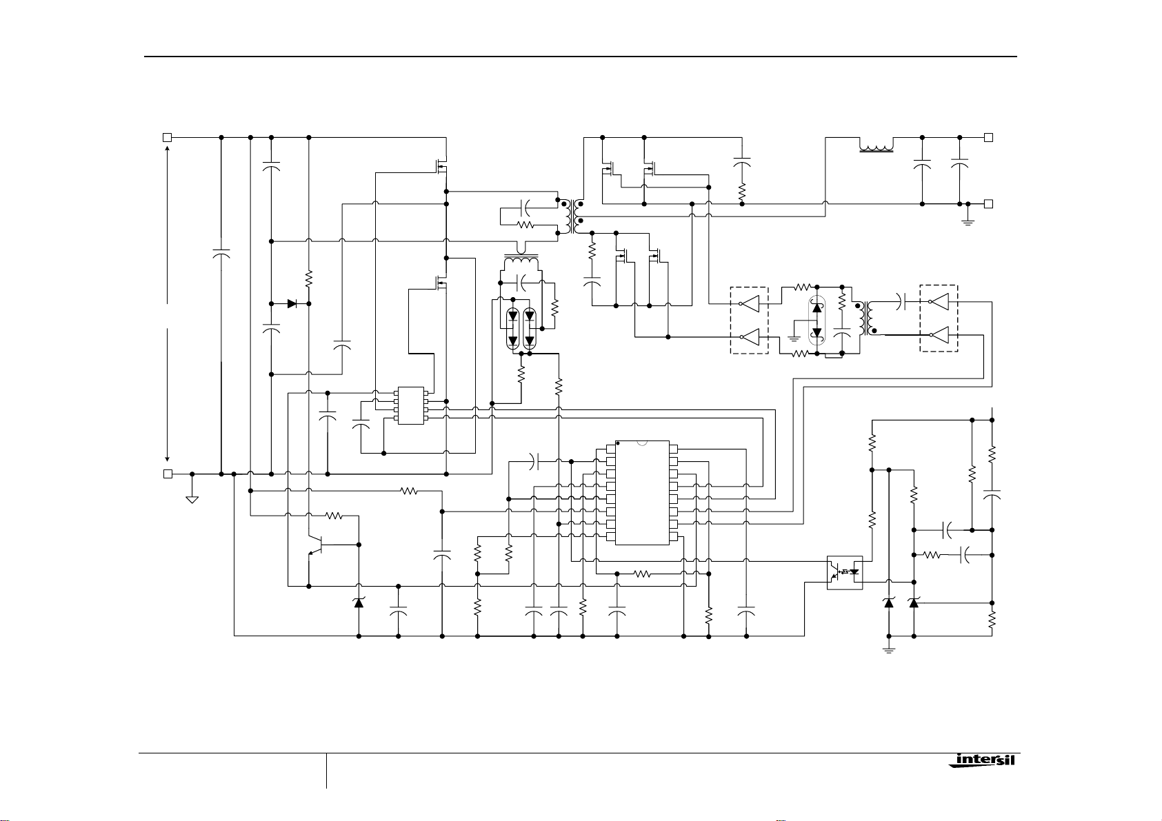
典型應用電路 – 電信原邊半橋式同步整流轉換器
VIN+
Q1
C2
C1
U1
HIP2100
VDD
VSS
HB
HO
HS
R3
Q2
LO
LI
HI
R5
C8
R1
CR3
36-75V
C3
VIN-
C7
C4
C5
R2
Q7
ISL6742
L1
Q3
Q5
C15
R13
T2
C14
CR1
C13
R6
T1
Q4
Q6
R17
C17
R9
CR2
R8
R7
U2
ISL6742
1
VREF
2
VERR
3
RTD
4
CT
5
FB
6
RAMP
7
CS
89
IOUT GND
16
SS
15
VADJ
14
VDD
OUTA
13
OUTB
12
11
OUTAN
10
OUTBN
R11
C16
R16
R25
R15
CR4
U6
R14
T3
C24
R19
R18
+
C22
EL7212EL7212
C18
U5
R20
C20
R21
+VOUT
C23
RTN
+VOUT
R22
R23
C19
C21
VR1
C6
R4
C9
R10
C11
C10
C12
R12
U3
VR2
U4
TL431
R24
3
Page 4
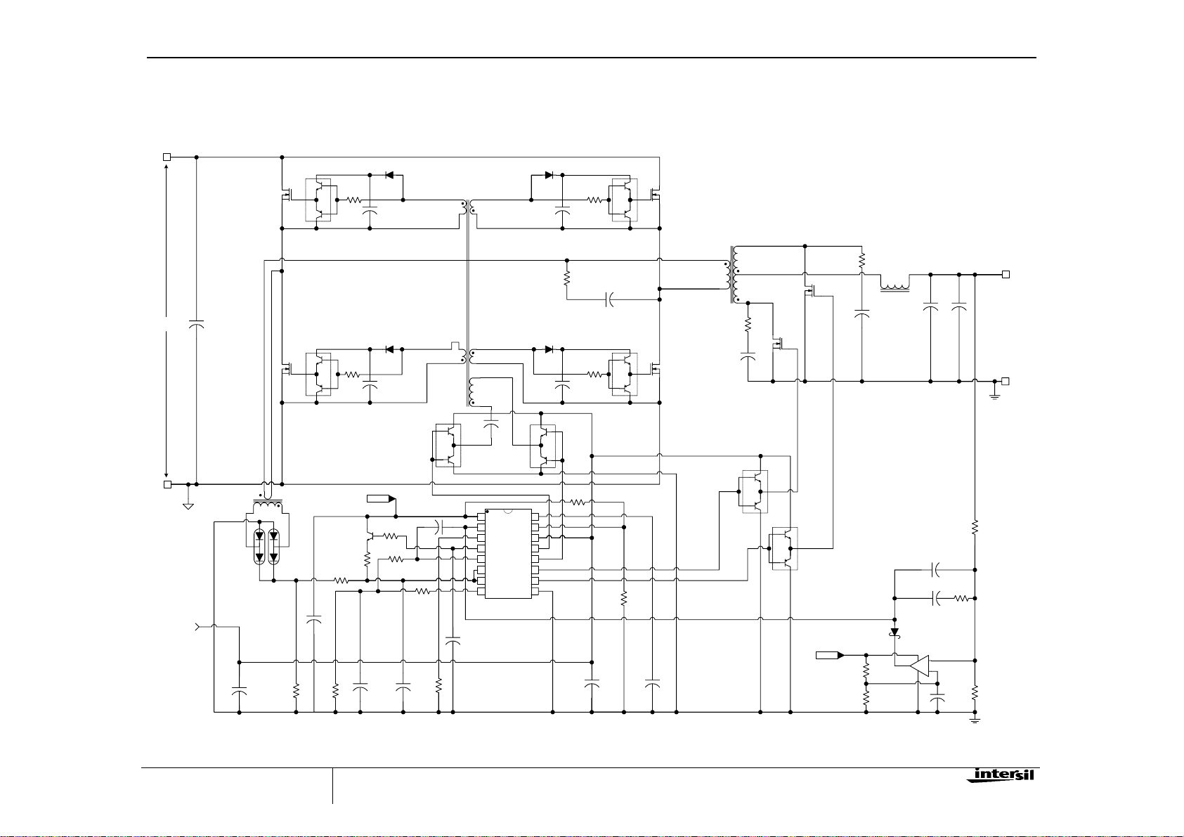
典型應用電路 – 高壓輸入次邊控制 ZVS 全橋轉換器
VIN+
ISL6742
400 VDC
VIN-
SECONDARY
BIAS SUPPLY
+
C1
T2
CR1 CR2
C2
Q1
Q5A
Q5B
Q4
Q7A
Q7B
R6
C3
R2
R3
CR4
R13
C9
CR6
R12
C8
VREF
R21
Q15
R9
C4
C12
R7
R8
R5
C5
T3
Q11A
Q11B
1
VREF
2
VERR
3
RTD
4
CT
5
FB
6
RAMP
7
CS
89
IOUT GND
C13
C6
CR3
R15
CR5
Q12A
Q12B
SS
16
VADJ
15
VDD
14
ISL6742
OUTA
13
OUTB
12
OUTAN
11
OUTBN
10
U1
R14
C10
R11
C7
R10
C14
Q2
Q6A
Q6B
T1
R16
Q16
C11
Q3
Q8A
Q8B
R4
C15
R17
C18
Q15
Q13A
Q13B
Q14A
Q14B
VREF
R22
R23
L1
C21
C19
C20
CR7
U3
+
C17
C16
R18
-
+
C22
+ Vout
RETURN
R20
R19
4
Page 5
ISL6742
額定值
Supply Voltage, VDD ----------------GND - 0.3V to +20.0V
OUTxxx ------------------------------------GND - 0.3V to VDD
Signal Pins-------------------------GND - 0.3V to V
VREF ---------------------------------------GND – 0.3V to 6.0V
REF
+0.3V
Peak GATE Current ----------------------------------------- 0.1A
ESD Classification
Human Body Model (Per MIL-STD-883 Method 3015.7)------2000V
Charged Device Model (Per EOS/ESD DS5.3, 4/14/93)-------1000V
熱性能的資料
Thermal Resistance Junction to Ambient (Typical) θJA (oC/W)
16 Lead QSOP (Note 1)-------------------------------------95
Maximum Junction Temperature -------------------55
Maximum Storage Temperature Range-----------65
Maximum Lead Temperature (Soldering 10s)--------------300
o
C to 150oC
o
C to 150oC
o
C
(QSOP – Lead Tips Only)
運行條件
Supply Voltage Range (Typical)------------------9V-16VDC
Temperature Range
ISL6742AAxx------------------------------ -40
CAUTION: Stress above those listed in “Absolute Maximum Ratings” may cause permanent damage to the device. This is a stress only rating and operation of the
device at these or any other conditions above those indicated in the operational section of this specification is not implied.
Notes:
1) θJA is measured with the component mounted on a low effective thermal conductivity test board in free air. See Tech Brief TB379 for
details.
2) All voltages are with respect to GND.
電气規范
Recommended Operating Conditions, Unless Otherwise Noted. Refer to Block Diagram and Typical Application Schematic.
o
C to 105oC
9V < V
DD
Electrical Specifications
< 20V, RTD = 10.0kΩ, CT = 470pF, TA = -40oC to 105oC (Note 3), Typical values are at TA= 25oC.
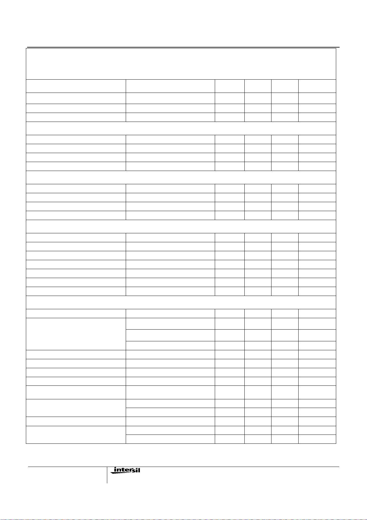
PARAMETER TEST CONDITIONS MIN TYP MAX UNITS
SUPPLY VOLTAGE
Supply Voltage - - 20 V
Start-Up Current, IDD VDD = 5.0V - 175 400
Operating Current, IDD R
LOAD
, C
= 0 - 7.5 12 mA
OUT
µA
UVLO START Threshold 8 8.75 9 V
UVLO STOP Threshold 6.5 7 7.5 V
Hysteresis - 1.75 - V
REFERENCE VOLTAGE
Overall Accuracy I
= 0 - 10mA 4.85 5 5.15 V
VREF
Long Term Stability TA = 125°C, 1000 hours (Note 4) - 3 - mV
Operational Current (source) -10 - - mA
Operational Current (sink) 5 - - mA
Current Limit VREF = 4.85V -15 - -100 mA
CURRENT SENSE
Current Limit Threshold VERR = VREF 0.97 1 1.03 V
CS to OUT Delay Excl. LEB (Note 4) - 35 50 ns
Leading Edge Blanking (LEB) Duration (Note 4) 50 70 100 ns
CS to OUT Delay + LEB TA = 25°C - - 130 ns
CS Sink Current Device Impedance VCS = 1.1V - - 20
Input Bias Current VCS = 0.3V -1.0 - 1.0
Ω
µA
5
Page 6
電气規范
Recommended Operating Conditions, Unless Otherwise Noted. Refer to Block Diagram and Typical Application Schematic.
9V < V
PARAMETER TEST CONDITIONS MIN TYP MAX UNITS
IOUT Sample and Hold Buffer Amplifier
Gain
IOUT Sample and Hold VOH
IOUT Sample and Hold VOL
RAMP
ISL6742
Electrical Specifications
< 20V, RTD = 10.0kΩ, CT = 470pF, TA = -40oC to 105oC (Note 3), Typical values are at TA= 25oC. (continued)
DD
= 25°C 4 4.09 4.15 V/V
T
A
= 1.00V, I
V
CS
= 0.00V, I
V
CS
= -300µA
LOAD
= 10µA
LOAD
3.9 - - V
- - 0.3 V
RAMP Sink Current Device Impedance V
= 1.1V - - 20
RAMP
Ω
RAMP to PWM Comparator Offset TA = 25°C 65 80 95 mV
Bias Current V
= 0.3V -5 - -2
RAMP
µA
Clamp Voltage (Note 4) 6.5 - 8 V
SOFT-START
Charging Current SS = 3V -60 -70 -80
µA
SS Clamp Voltage 4.41 4.5 4.59 V
SS Discharge Current SS = 2V 10 - - mA
Reset Threshold Voltage TA = 25°C 0.23 0.27 0.33 V
ERROR AMPLIFIER
Input Common Mode (CM) Range (Note 4) 0 - VREF V
GBWP (Note 4) 5 - - MHz
VERR VOL I
VERR VOH I
= 2mA - - 0.4 V
LOAD
= 0mA 4.2 - - V
LOAD
VERR Pull-Up Current Source VERR = 2.50V 0.8 1 1.3 mA
EA Reference TA = 25°C 0.594 0.6 0.606 V
EA Reference + EA Input Offset Voltage 0.59 0.6 0.612 V
PULSE WIDTH MODULATOR
Minimum Duty Cycle VERR < 0.6V - - 0 %
Maximum Duty Cycle (per half-cycle)
VERR = 4.20V, V
(Note 5)
RTD = 2.00kΩ, CT = 220pF
RTD = 2.00kΩ, CT = 470pF
= 0V, VCS = 0V
RAMP
94 %
- 97 -
%
- 99 - %
Zero Duty Cycle VERR Voltage 0.85 - 1.2 V
VERR to PWM Comparator Input Offset TA = 25°C 0.7 0.8 0.9 V
VERR to PWM Comparator Input Gain 0.31 0.33 0.35 V/V
Common Mode (CM) Input Range (Note 4) 0 - 4.45 V
OSCILLATOR
Frequency Accuracy, Overall
(Note 4) 165 183 201 kHz
-10 - 10 %
Frequency Variation with VDD TA = 25°C, (F
Temperature Stability
6
VDD = 10V, |F
|F
– F
0°C
105°C
- - F
)/F
20V
- F
-40°C
|/F
(Note 4) - 1.5 - %
25°C
- 0.3 1.7 %
10V
10V
|/F
- 4.5 - %
0°C
0°C
Page 7

ISL6742
Electrical Specifications
電气規范
Charge Current TA = 25°C, VCS = 1.8V -193 -200 -207
Discharge Current Gain 19 21 23
CT Valley Voltage Static Threshold 0.75 0.8 0.88 V
CT Peak Voltage Static Threshold 2.75 2.8 2.88 V
CT Pk-Pk Voltage Static Value 1.92 2 2.05 V
RTD Voltage 1.97 2 2.03 V
OUTPUT
Recommended Operating Conditions, Unless Otherwise Noted. Refer to Block Diagram and Typical Application Schematic.
< 20V, RTD = 10.0kΩ, CT = 470pF, TA = -40oC to 105oC (Note 3), Typical values are at TA= 25oC.
9V < V
DD
µA
µA/µA
High Level Output Voltage (VOH) I
Low Level Output Voltage (VOL) I
Rise Time C
Fall Time C
UVLO Output Voltage Clamp VDD = 7V, I
Output Delay/Advance Range
OUTAN/OUTBN relative to OUTA/OUTB
= -10mA, VDD - VOH - 0.5 1 V
OUT
= 10mA, VOL - GND - 0.5 1 V
OUT
= 220pF, VDD = 15V (Note 4) - 110 200 ns
OUT
= 220pF, VDD = 15V (Note 4) - 90 150 ns
OUT
= 1mA (Note 6) - - 1.25 V
LOAD
V
= 2.50V (Note 4) - - 3 ns
ADJ
V
< 2.425V -40 - -300 ns
ADJ
> 2.575V 40 - 300 ns
V
ADJ
Delay Control Voltage Range
OUTAN/OUTBN relative to OUTA/OUTB OUTxN Delayed 2.575 - 5 V
OUTx Delayed 0 - 2.425 V
VADJ Delay Time
TA = 25°C (OUTx Delayed)
VADJ = 0 280 300 320 ns
VADJ = 0.5V 92 105 118 ns
VADJ = 1.0V 61 70 80 ns
VADJ = 1.5V 48 55 65 ns
VADJ = 2.0V 41 50 58 ns
TA = 25°C (OUTxN Delayed)
VADJ = VREF 280 300 320 ns
VADJ = VREF - 0.5V 86 100 114 ns
VADJ = VREF - 1.0V 59 68 77 ns
VADJ = VREF - 1.5V 47 55 62 ns
VADJ = VREF - 2.0V 41 48 55 ns
THERMAL PROTECTION
Thermal Shutdown (Note 4) 130 140 150 °C
Thermal Shutdown Clear (Note 4) 115 125 135 °C
Hysteresis, Internal Protection (Note 4) - 15 - °C
NOTES:
3. Specifications at -40
o
C and 105 oC are guaranteed by 25
o
C test with margin limits.
4. Guaranteed by design, not 100% tested in production.
5. This is the maximum duty cycle achieveable using the specified values of RTD and CT. Larger or smaller maximum duty cycles may be
obtained using other values for these components. See Equation 1-3.
6. Adjust VDD below the UVLO stop threshold prior to setting at 7V.
7
Page 8

ISL6742
0
0
0
)
0
典型性能曲線圖
1.02
1.01
REF
1
NORMALIZED V
0.99
0.98
-40 -25 -10 5 20 35 50 65 80 95 11
°
1 REFERENCE VOLTAGE vs. TEMPERATURE FIGURE 2 CT DISCHARGE CURRENT GAIN vs RTD CURRENT
FIGURE
4
1•10
25
24
23
22
21
20
19
CT DISCHARGE CURRENT GAIN
18
0 200 400 600 800 100
3
1• 1 0
3
1•10
100
DEADTIME (ns)
10
0 1020304050 6070809010
RTD (k
Ω
CT =
1000pF
680pF
470pF
330pF
220pF
100pF
100
FREQ UENCY (kHz)
10
0.1 1 1
RTD=
10k
50k
100k
Ω
Ω
Ω
FIGURE 3 DEADTIME (DT) vs CAPACITANCE FIGURE 4 DEADTIME (DT) vs FREQUENCY
8
Page 9

各管腳簡介
VDD
VDD是控制器的電源輸入端。要优化抗扰度, 用一個陶瓷電容
器盡可能靠近并挎接在VDD和GND引腳。
監測VDD是用來做輸入電源欠壓保護 (UVLO)。起動和切斷的
臨限會密切跟隨以保證固定的磁滯。
GND
ISL6742
VADJ
這個引腳從0V到5V的控制電壓設置OUTA/OUTB和
OUTAN/OUTBN相對延遲或者前置。
相對于OUTA/OUTB, 電壓低于2.425V會導致
OUTAN/OUTBN相對前置。相對于OUTA/OUTB, 電壓高于
2.575V會導致OUTAN/OUTBN相對延遲。電壓值為2.50 V
±75mV會導致零相位差。如果這個輸入端懸浮, 從VREF分壓
50%的內部電壓會導致無延遲相位。
器件上所有功能和電源地都以這個引腳為基准。由于高峰值
電流以及高頻運行, 低阻抗布局是很有必要的。高度推荐使用
接地面以及短線跡。
VREF
這是5.00V的基准電壓輸出端,且有3%的容差遍及輸入、負
載和溫度范圍。可連接0.1µF至2.2µF的低ESR電容至GND以
作濾波這輸出所需。
CT
振蕩器的定時電容可以挎接在這個引腳和GND之間。這個電
容是用200µF 的內部電流源來充電, 其放電是通過用戶可以調
整的RTD設置的電流源。
RTD
這是振蕩器的定時電容的放電電流制引腳。跨接在這引腳和
GND的電阻的電流決定CT放電電流的大小。CT放電電流通
常是電阻電流的20倍。這個PWM的死區時間是由定時電容的
放電期間來決定的。在RTD引腳的標稱電壓是2.00V。最小的
可用RTD阻值為2kΩ。
相位延遲/前置的范圍是0或者是40ns与300ns之間, 隨著与
2.5V電壓差的增加, 相位差也會增大。控制電壓与相位差的關
系是非線性的。當控制電壓接近2.5V時, 電壓增益(∆t/∆V)是很
小的, 并且會隨著電壓接近控制极限而很快地增大。當選擇一
個相當短的延遲/前置時, 這個特點為用戶提供不斷的准确
性。
IOUT
這是取樣及保存電路的4倍緩沖放大器的輸出端。這個電路是
用來攫取及平均CS信號。
RAMP
這是PWM比較器的鋸齒波的輸入端。在PWM信號中斷時, 這
個引腳會与GND短路。這個輸入信號必須是鋸齒波型。如果
是電流模式控制, 這個引腳必須直接与CS引腳相接, 同時, 電
流環路的反饋信號也應与兩個輸入端相接。如果是電壓模式
控制, 這個鋸齒型振蕩波可以被緩沖后用來產生合适的信號,
或者, RAMP引腳可以通過RC网絡与輸入電壓相連以取得正
向饋電控制效果; 或者, RAMP引腳也可以通過RC网絡与
VREF導通來產生所需的鋸齒波型。
CS
這是過流比較器以及平均電流取樣及保存電路的輸入端。過
流比較器的標稱臨限值設置在1.00V。PWM輸出的任一端被
終止會導致CS引腳与GND引腳短路。
取決于電流取樣的內部阻抗,由于內部時鐘与外部電源開關
之間的延遲, 可以在輸入端串聯一個電阻。這個延遲有時會導
致CS引腳在電源開關器件關斷之前被放電。
OUTA and OUTB
這兩個PWM輸出端是用來控制FETs交替式運行。
OUTAN and OUTBN
這些輸出端与OUTA和OUTB成互補。這些輸出端可以用來控
制同步整流器。每個輸出端与其互補端的相位關系是由VADJ
的電壓值來控制的。
9
FB
這是誤差信號放大器的反相輸入端。這個放大器可以用來作
電壓反饋的誤差信號放大, 也可以用來作平均限流放大器。如
果這個放大器沒有被使用, FB引腳應与GND短路。
VERR
VERR引腳是誤差信號放大器的輸出端并且是PWM比較器的
反相輸入端。反饋補償的元件可以接在VERR引腳与FB引腳
之間。VERR具有額定值為1mA上拉電流源。在VERR信號
上作電壓鉗位可以用來實現軟啟功。
當VERR電壓小于0.6V時, OUTA和OUTB輸出端的工作周期
減少到0%。与此同時, OUTA和OUTB的互補輸出端, OUTAN
和OUTBN的工作周期將增加到100%。
SS
Page 10
ISL6742
S
S
S
⋅
S
在這個引腳与GND之間連接一個軟啟動時序電容能夠控制軟
啟動的時間。這個電容值能夠決定在啟動時工作同期上升的
速度。為了提高無噪聲干扰, 建議使用至少100pF的電容, 盡
管沒有最小電容的要求。
通过一个小晶体管的集电极(漏极)开路方式与GND短路, SS引
脚也可以用来禁止输出电压的上升。
功能概述
主要特點
ISL6742最适用于需用精确占空比和死區控制的低成本橋型和
推挽型拓扑結构的變換器。它有許多保護和控制的性能, 需要
极少外部元 件。其 性能包括: 電流模式或電壓模式控制, 可調
軟啟動, 峰值和平均過流保護, 過熱保護, 可調延遲或增加時間
的同步整流器輸出, 和可調振蕩器頻率。
振蕩器
ISL6742通過改變電阻和電容可調振蕩器頻率高達2MH。開
關周期是定時電容充電和放電時間之和。充電時間由CT和內
部200µA電流源決定,而放電時間取決于RTD 和CT
TC11.5 1 0
T
0.0 6 R T D CT
≈
D
T
SW
式中: TC 和 TD分別是充電和放電時間, TSW是振蕩器周期; F
是振蕩器頻率。ISL6742是一雙端控制器,一個輸出的開關周
期等于二個振蕩器周期。由于每個傳輸延遲約為10ns,因此
實際時間比所計算的時間稍微長。這個延遲直接增加到開關
時間,且引起定時電容峰值和谷電壓門限過沖,因而增大了
定時電容峰-峰的電壓。另外,如果使用非常低的充電和放電
電流,時間誤差將會因CT引腳處的輸入阻抗而增加。
3
CT
⋅
⋅≈
⋅⋅()
TCTD+
EQ. 1
50 10
+
⋅
1
---- -- -- --==
F
SW
EQ. 3
9–
。
EQ. 2
SW
啟動時,軟啟動電路限制誤差電壓(VERR)等于軟啟動電壓。
輸出脈寬隨著軟啟動電容電壓增加而增加,這使軟啟動期間的
占空比可從零增加到調整脈寬。當軟啟動電壓超過誤差電
壓,軟啟動完成。軟啟動開始于起動或因故障而复位時。軟
啟動充電時間可用下式計算:
t64.3C
=m
式中: t 是充電時間,其單位為 mS;C 是軟啟動電容,其單
位為µF。軟啟動時間通常少于或等于此值,取決于什么時候
反饋環得到控制。軟啟動電壓鉗位于 4.50V,±2%總容差。
它适用于電流需保持低于 70µA 充電電流的軟啟動。
用 SS 引腳為輸入失效端來實現輸出截止。把 SS 拉低于
0.25V 使所有輸出降低。用漏极開路方式聯接失效信號于 SS
引腳。
EQ. 6
門极驅動器
ISL6742的輸出可灌出和吸入10mA電流(在額定的VOH, VOL),
應連接于高電流的MOSFET門极驅動器或分立式的雙极推拉
驅動器。 典型的輸出電阻是50Ω。
過流運作
電源供應設計可用兩种過流保護方法。第一种方法是反應快
的周期式峰值電流保護。第二种方法是一种可產生不變或砌
牆式電流限制狀態的較慢和均衡的方法。如果設計是用電壓
模式控制,平均過流保護可通過保持占空比對稱于1/2周期間
而保持變壓器磁性流量均衡。
CS引腳的電流感應信號連接于峰值電流比較器和取樣及保存
均衡電路。在導通期間及上升沿封鎖(LEB)延遲70ns后,電流
感應信號被取樣,确定周期的平均電流,且放大4倍輸出于
IOUT引腳。若RC濾波器設在CS輸入端,其時間常數應不超
出約50ns,否則IOUT會出現重大誤差。
最大占空比(D
計算:
T
C
D
-----------=
T
SW
DT 1 D–=
)和死區時間百分比(DT)可用以下公式
MAX
EQ. 4
EQ. 5
實現軟啟動運作
ISL6742 使用外部電容和內部電流電源來作軟啟動。軟啟動
降低啟動期間的電壓和浪涌電流。
Channel 1 (yellow): OUTA Channel 2 (red): OUTB
10
Page 11

ISL6742
π
⋅
z
Channel 3 (blue): CS Channel 4 (green): IOUT
FIGURE 5 CS INPUT vs IOUT
圖5顯示了在穩定狀態下CS信號和IOUT之間的關系。IOUT為
4倍的CS平均數。圖6顯示了外部正弦波調整CS時均流電路
的動態。在輸出脈沖終止時,IOUT會由取樣及保存電路重新
調整。
FIGURE 6 DYNAMIC BEHAVIOR OF CS vs IOUT
IOUT代表精确的平均電流信號只要輸出電感電流是連續的
(CCM運行)。一旦電感電流成為不連續的運行(DCM運行),
IOUT輸出的是1/2峰值電感電流而不再是平均電流。這是因為
取樣及保存電路只在開關導通期間運行。在關斷期間電感電
流達到零時就無法檢測出了。
若需平均過流限制,將IOUT分割至所需的振幅后和過濾于
ISL6742的誤差放大器。收效信號會輸入到電流誤差放大器
(IEA)。除IEA沒有電流源外,它類似大多數PWM控制器的電
壓誤差放大器(EA) ,但VERR有內部1mA的上拉電流源。
以內部0.6V為參考,配置IEA作為(型號I)集成放大器。FB与
0.6V 之間的誤差放大及過濾后產生的收效信號, VERR, 將与
RAMP的鋸齒電壓比較產生PWM信號。如果FB比0.6V少,
IEA會開環(斷開電源), VERR則會處于由電壓環所決定的電平,
且不影響占空比。IOUT會隨輸出負載增加而增加, 且FB的電
壓也會增加至0.6V。此時IEA會降低VERR以保持0.6V時的輸
出電流。當輸出電流再次下降低于平均電流門限值時, IEA又
回到開環狀態, 而占空比會由電壓環控制。
在典型的電源中,平均電流控制環除了調控的是電流而不是
電壓外,其運作如電壓控制環一樣。
如上所述,ISL6742的有效EA可用電壓EA作電壓反饋控制環
而不用電流EA。電流或電壓EA可用一外部操作安培阻止電流
流入VERR。 外部EA必須只吸入電流, 可通過加接一個二极
管于其輸出端來實現。
4 倍的檢驗品和舉行緩沖增益可產生150 - 1000mV的峰值CS
信號, 取決于IOUT的電阻分割器。平均電流環的總帶寬則由
總電流EA 補償和IOUT的分割器所确定。
150 - 1000 mV
C10
1
ISL6742
2
VERR
3
4
FB
0.6V
CS
IOUT
S&H
4x
-
+
5
6
7
89
R6
R5
R4
16
15
14
13
12
11
10
FIGURE 7 AVERAGE OVERCURRENT IMPLEMENTATION
假設 R6 >>(R4 || R5),電流 EA 交界頻率為
1
---------------------------------
=H
f
CO
2
R6 C10
式中 f
⋅
是交界頻率。可并聯一電容于 R4 以作雙极過濾。
CO
EQ. 7
平均電流環帶寬通常設置為少于開關頻率,典型地少于 5kHz
或几百赫茲。尤其适用于大浪涌電流的應用。平均電流環可
設置穩定過流門限和比所需瞬變較長的時間。峰值電流限制
可設高于所需瞬變,這樣就不會受瞬變的干扰,但仍需防止
短期的較大故障。實質上可有 2 個階段的過流反應。
峰值過流狀況類似于大多數 PWM 控制器。若峰值電流超過
1.0V,輸出脈寬會立刻終止。
如果電壓模式控制用于橋型拓扑結构,應注意峰值電流限制
會導致不穩定操作。電壓模式橋型拓扑結构的 DC 鎖電容會
不均衡,如變壓器磁芯的流量。平均過流電路通過保持每 1/2
周期的占空比對稱來防止這种狀況。如果不用平均電流限制
電路,建議用外部元件來鎖住過流關斷的方法。
CS 到輸出傳播延遲會因上升沿封鎖(LEB)的間隔而增加。有
效延遲是兩個延遲之和,最大值為 130ns。
電壓前饋操作
電壓前饋是用以調整輸出電壓因輸入電壓變化而沒有控制環
干預的一种技巧。電壓前饋常用于電壓模式控制環,但是不
需用于峰值電流模式控制環。
11
Page 12
ISL6742
()
S
電壓前饋操作是通過調整鋸齒斜坡与輸入電壓的直接比例來
實現。舉例如圖8。
VIN
ERROR VOLTAGE
RAMP
CT
OUTA, B
FIGURE 8 VOLTAGE FEED FORWARD BEHAVIOR
輸入電壓前饋可用RAMP輸入來實現。在輸入電壓和接地之
間連接一RC网絡, 如圖9所示, 會產生一個与源電壓的振幅成
比例的電壓斜坡。在輸出脈沖的終止時把RAMP釋放到接地
以產生反复的鋸齒波。RAMP鋸齒波与VERR電壓的比确定占
空比。RC元件的選擇取決于所需輸入電壓范圍和振蕩器的頻
率。選用适合的RC元件使在半周期內最低輸入電壓的斜坡振
幅達到1. 0V。
式中 t 等于振蕩器時間減去死區時間。如果死區時間少于振蕩
器時間,可忽略此項計算。
電壓前饋實現時會有一伏特鉗于變壓器。最大的占空比由較
少的振蕩周期或RAMP充電時間所确定,RAMP充電時間隨輸
入電壓增加而減少,并相應地限制占空比。
如果不需要前饋操作,可連接RC网絡于VREF或一緩沖CT信
號,而不是輸入電壓。恰當的PWM操作需要在RAMP上產生
一鋸齒波。
實現同步化
外部時鐘信號同步可用如沒有分隔的同步輸入的PWM控制器
的同樣方法來實現。加設一短脈沖橫跨于与定時電容相連的
小電阻,可使振蕩器鋸齒波提前終止。
CT
Rs
1
2
3
4
CT
5
ISL6742
6
7
89
16
15
14
13
12
11
10
GND
FIGURE 9 VOLTAGE FEED FORWARD CONTROL
參見圖9,斜坡電容的充電時間為
V
tR3C71
–=
⋅⋅
------------------------------------–
ln
要達到最佳效果,電容的最大值應限制在10nF。通過電阻的
DC電流應限制為3mA。例如,若振蕩器頻率是400kHz,最小
輸入電壓是300V,選擇4.7nF的斜坡電容,整理公式8可求得
電阻值。
---- -- ---- -- -- -- -- -- -- -- -- -- -- -- -- ---- -- -- -- -- -- -- -- -- -- -- -- -- -----
R3
==
C7 1
ln
⋅
159=k
t–
V
RAM P PE AK
------------------------------------–
V
IN MIN
Ω
EQ. 9
()
RAMP PEA K
V
IN MIN
()
)()
EQ. 8
2.5–10
---- -- ---- -- -- -- -- -- -- -- -- -- -- -- -- -- -- -- -- -- -- -- -- -- -- --
4. 7 10
⋅⋅
6–
⋅
9–
1
ln
-- -- -----–
30 0
1
FIGURE 10 SYNCHRONIZATION TO AN EXTERNAL CLOCK
所加的脈寬應少于鋸齒波釋放時間。
同步整流器輸出和控制
ISL6742具有雙端PWM輸出,OUTA和OUTB;和同步整流器
(SR)輸出,OUTAN和OUTBN。SR輸出是PWM輸出的補碼
。補碼輸出應連接于PWM輸出的反方向,例如,OUTA和
OUTBN是一對,OUTB和OUTAN是一對。
參見圖11,SRs交替開通于周期的自由運行期間(OUTA/B關
斷),OUTA或OUTB在一個開通時其另一個是關斷的。如果
OUTA開通,相應地SR必須是導通的,這表示OUTBN的SR
控制信號正确。同樣地,如果OUTB開通,相應地SR必須是
導通的,這表示OUTAN的SR控制信號正确。
12
Page 13
FIGURE 11 BASIC WAVEFORM TIMING
π
π
ISL6742有一非常有用的性能就是可調PWM輸出 (OUTA,B)
和它們的補碼(OUTAN,BN)相位關系間隔±300ns。這一性能
允許補償PWM FETs和SR FETs間的信號傳播延遲的差异。
而供應到VADJ的電壓控制相位關系。圖12和13顯示了這延遲
關系。
ISL6742
設 VADJ 為 VREF/2 是沒有任何輸出延遲。沒有延遲電壓會
有±75mV 容差窗口。控制電壓低于 VREF/2 零延遲門限會引
起 PWM 輸出 OUTA/B 延遲。控制電壓高于 VREF/2 零延遲
門限則會引起 SR 輸出 OUTAN/BN 延遲。值得注意的是當
PWM 輸出 OUTA/B 延遲,CS 到輸出傳播延遲會因這延遲的
增加而增加。
通常在一組信號橫跨原邊-副邊隔离范圍時 PWM 和 SR 輸出
間的傳播延遲會不相符,而這延遲功能就是用以補償這不相
符的傳播延遲。根据需要可用外部電阻,電容和二极管來擴
張或壓縮個別的輸出脈沖。
斜率补偿
峰值電流模式控制需要用斜率補償來改善噪音干扰,在低負
載時可阻止電流環的不穩定,特別是占空比高于50%時。可
通過加接一外部斜坡到反饋電流信號或在反饋電壓誤差信號
減接一外部斜坡來實現斜率補償。加接一外部斜坡到反饋電
流信號是較為常用的方法。
小信號電流型[1]顯示了自然抽樣調制器的增益。Fm,無斜率
補償,是
FIGURE 12 WAVEFORM TIMING WITH PWM OUTPUTS
DELAYED, 0V < VADJ < 2.425V
1
------------------=
Fm
SnTsw
EQ. 10
式中:Sn是鋸齒信號的斜率。Tsw是半周時間。若加接一外
部斜坡,調制器的增益則為
Fm
----------------------------------Sn Se+
()
1
Tsw
1
-------------------------==
SnTsw
m
c
EQ. 11
式中:Se是外部斜坡的斜率以及
mc1
Se
------+=
Sn
EQ. 12
50%的振蕩器頻率的雙极阻尼系數決定外部斜坡的基准額。
若Q系數設置為1,雙极會臨界阻尼;Q > 1時,過阻尼; Q <
1則會欠阻尼。欠阻尼會引起電流環不穩定。
------------------------------- ----------------
Q
=
π
1
1D–
m
()
()
c
0.5–
EQ. 13
式中:D是半周期時間的占空比。設定Q = 1求得Se為
SeS
=
1
---0.5+
n
1
-------------1–
1D–
EQ. 14
Sn和Se分別是電流斜坡和外部斜坡導通時的斜率,与導通時
間(T
) 之積是導通時間(TON) 內所產生的電壓變化。
ON
1
FIGURE 13 WAVEFORM TIMING WITH SR OUTPUTS
DELAYED, 2.575V < VADJ < 5.00V
13
VeV
---0.5+
=
n
1
-------------1–
1D–
EQ. 15
Page 14

ISL6742
V
V
Ω
m
A
V
m
V
Ω
式中:Vn是導通時間內反饋電流信號的變化,Ve是加外部斜
坡所增加的電壓。用輸入電壓,電流傳感器元件和輸出電感
可求出Vn, 代入等式12, 可求出Ve。
=
V
e
TSWV
-- -- -- -- -- -- -- - - -- -- - - ---- -- -- -- -- -- --
⋅
N
CTLO
R
N
⋅
CS
O
⋅
1
S
--- D 0 . 5–+
-- -- ---
⋅
N
π
P
EQ. 16
式中:RCS是電流感應電阻,NCT是電流變壓器線圈比例,L
是輸出電感,VO是輸出電壓,而NS和NP分別是副邊和原邊線
圈。
電感電流通過隔离變壓器和電流感應變壓器的反射而在感應
電阻上產生的反饋電流信號為
V
CS
NSR
=
-- -- -- -- -- ---- -- -- -- -- I
N
PNCT
⋅
CS
⋅
DT
⋅
O
SW
--------------------V
+
2L
O
N
IN
S
-------⋅VO–
N
P
EQ. 17
式中:VCS是橫跨電流感應電阻的電壓,IO是輸出電流的門限
值。
由于峰值電流門限值是1.00V,總反饋電流信號和外部斜坡電
壓必須加到這個伏數。
VeVCS+1=
EQ. 18
代入等式16和17到等式18,所得的RCS為
NPN
⋅
R
=
CS
CT
---------------------N
S
---------------------------------------------------
⋅
I
O
+
V
O
------- T
L
O
1
1
D
---
----+
SW
2
π
EQ. 19
上述的討論只用了理想的元件,但在決定外部斜坡所加的數
額時必須考慮磁化電感的影響。磁化電感在反饋電流信號設
了一斜坡補償幅度并減低外部斜坡的所需值。磁化電感加上
原邊電流超出了副邊的電感電流。
DT
V
⋅
IN
I
-- -- -- -- -- ---- -- -- -- -- - - -- -- --=
∆
P
SW
L
EQ. 20
式中:VIN是占空比D的輸入電壓,Lm是原邊磁化電感。電流
感應電阻 (R
V
∆
CS
) 的磁化電流效果是
CS
I
∆
⋅
PRCS
-- -- -- -- -- ---- -- -- -- -- -=
N
CT
EQ. 21
若VCS大于或等于Ve,則不需要額外斜坡補償,而RCS為
N
------------------------------------------------------------------------------------------------------------------------------=
R
CS
N
S
-- -- - --I
N
P
DT
-- -- ---- -- -- -- - V
+
O
2L
SW
O
⋅
CT
N
IN
S
-------⋅VO–
N
P
⋅
V
⋅
INDTSW
-- -- -- -- -- -- -- -- -- -- -- -- -- -- --+
L
EQ. 22
若VCS小于Ve,則仍可用等式16計算RCS值,但含外部斜坡的
斜坡補償額必須減去V
CS
。
ISL6742可用外部緩沖和CT信號來實現加斜坡補償。此緩沖C
T信號与電流感應反饋的和外加于CS引腳, 如圖14所示。
1
VREF
2
ISL6742
3
4
O
R9
R6
R
CS
FIGURE 14 ADDING SLOPE COMPENSATION
C4
CT
5
6
7
CS
89
CT
16
15
14
13
12
11
10
假設設計時選擇將RC過濾器(R6和C4)放在CS引腳, 加在外部
斜坡 的R9值可疊加得
2D R6
V
V
–
∆
e
CS
---------------------=
R6 R9+
⋅
EQ. 23
重新整理,求得R9為
2D V
()
----------------------------------------------------------
R9
=
+–
∆
e
V
V
–
∆
e
R6
V
⋅
CS
CS
EQ. 24
用等式19計得的RCS值必須重新調節,樣CS引腳的電流感應
信號可由等式17推算出。這主要是由于R6和R9形成分阻器。
R6 R9+
=
′
CS
---------------------R
R9
⋅
CS
EQ. 25
R
例如:
= 280V
V
IN
= 12V
V
O
L
= 2.0µH
O
Np/Ns = 20
Lm = 2mH
I
= 55A
O
振蕩器頻率, Fsw = 400 kHz
占空比, D = 85.7%
N
= 50
CT
R6 = 499Ω
用等式19求出電流感應電阻,RCS
= 15.1Ω
R
CS
用等式16确定加在反饋電流信號的電壓值,V
e
Ve = 153mV
14
Page 15

ISL6742
接著,用等式21确定磁化電流的效果
= 91mV
∆V
CS
運用等式24求出從CT引腳到CS引腳的總和電阻, R9。
R9 = 13.2kΩ
用等式25确定新的R
R’
= 15.7Ω
CS
值,R’CS
CS
額外的斜坡補償可以用作設計余量。上述討論确定了所需的
最小外部斜坡。用在C
增設外部斜坡的緩沖晶体管要有足夠
T
高的增益(>200)才可減低所需的基流。但振蕩器頻率會因所
需基流降低流入C
的充電電流而降低。
T
均衡操作
ISL6742變換器的均衡操作可用平均電流信號IOUT來實現。
IOUT提供了非常准确的輸出電流且可用許多常用均流技術包
括主從電流均流方法和平均電流均流方法來實現均流。
由于IOUT表示平均電感電流(CCM操作),可減少因使用峰值電
感電流方法而產生的均流誤差。特別是消除因不相符的開關
頻率而產生的均流誤差。
主從電流均流方法說明如下圖15,
VOLTAGE ERROR AMPLIFIER
INVERTING (-) INPUT
U1
1
2
3
4
5
6
7
CS
89
IOUT
+
U2A
-
ISL6742
S&H
4x
R4
(>>R3)
VDD
16
15
14
13
12
11
10
R1
R3
FIGURE 15 MASTER-SLAVE CURRENT SHARING
USING AVERAGE CURRENT
在均衡和雙重保護的應用中,每個供應電源的 IShare 信號應
連接一起,每個供應電源在 IOUT 產生一電壓与平均輸出電
流成比例,且限制電阻 R3 在 IShare。最高 IShare 信號(和最
大輸出電流)的單元輸出電流到 IShare 總線,此單元為主單
15
BIAS
R2
(>>R1)
C1
R5
(>>R1)
-
U2B
+
DISCONNECT IF P/S FAILS
OR IS TURNED OFF
VOUT
OUTPUT
VOLTAGE
FEEDBACK
DIVIDER
Q1
R7
R6
ISHARE
元。而較低 IShare 信號的單元不會輸出電流到 IShare,即為
從單元。每個從單元將主單元的 IShare 信號与其信號相比,
足夠的差异會導通 Q1 拉低反饋電壓。因反饋電的降低, 輸出
電壓會通過增加電壓來補償反饋環和增加輸出電流。每個從
單元會增加其輸出電壓直至其輸出電流大約等于主單元的。
主單元与從單元的輸出電流差异由 R1 和 R2 設置。要防止主
單元与從單元產生動擺, 需有差异。此差异也可在電源單獨操
作時阻止均流電路的運作。
從單元輸出的最大輸出電壓是由 R6 和輸出電壓反饋分割器控
制。輸出電壓增加的最大值一般限制在几個百分比,但必須
大于反饋与參考元件的容差和所有單元間的電壓下跌。若用
隔离感應,調整范圍必須包括電源供應輸出和隔离感應間電
壓下跌的差异。電流限制電路必須限制電壓變化少于輸出過
壓門限值, 否則會引發過壓限制。
放大器U2A設置IOUT到IShare的比例系數,和增大IShare的
電流供應能力。U2B則是設置相應頻率和均流電路增益的低
帶寬放大器。均流帶寬必須大大地低于電壓反饋環帶寬以确
保整体穩定。用R1和R5設置增益,R5和C1設置帶寬。
對于不需要故障隔离的動力系統可不用IShare的開關。通常
用MOSFET或JFET驅動可實。
平均電流模式控制
IOUT的平均電流信號也可用于平均電流模式控制而不是峰值
電流模式控制。平均電流模式控制有許多优點,尤其是改善
噪音干扰和電流反饋環補償的設計高度靈活。如圖16 所示。
IOUT VOUT
OFFSET
R2
VOLTAGE ERROR
U1
AMPLIFIER
C1
-
+
REF
R1
Rb
VERR
C2
U2
+
CURRENT ERROR
AMPLIFIER
R3
-
R4
Figure 16 AVERAGE CURRENT MODE CONTROL
相比于峰值電流模式控制配置中的峰值電流感應信號,電壓
放大器總輸出接近平均輸出電流。電壓環補償和電流環補償
可單獨調整。
電壓誤差放大器可調整供應的平均輸出電流,其最大輸出電
平決定最大輸出電流。無論IOUT或電壓EA輸出都必須适當地
按比例增減以達到所需的電流門限設點。圖16所示的偏移電
壓是用以補償電流放大器的輸入偏移電壓以确保可達到零占
空比運作。
根据控制環的操作要求可用除上述之外的其他网絡補償。
Page 16

ISL6742
故障狀況
如果VREF或VDD跌落低于其欠壓鎖定(UVLO)門限值或触發
過熱保護就會發生故障狀況。檢測出故障時,軟啟動電容很快
地被放電且輸出就會截止。當故障清除后以及軟啟動電壓低
于复位臨限時,一個軟啟動周期重新運作。過流狀況是不被認
為故障且不會導致關斷。
過熱保護
ISL6742持有內部的過熱保護。內熱傳感器保護器件芯片結溫
不超出140
o
C,而熱遲滯約15oC。
接地要求
為使這個器件能理想地工作,應該要仔細布局。特別是應用
一個好的接地面,VDD和VREF必須以一個好的高頻電容直接
旁接到地GND。
參考資料
Ridley, R., “A New Continuous-Time Model for Current
Mode Control”, IEEE Transactions on Power
Electronics, Vol. 6, No. 2, April 1991.
16
Page 17

ISL6742
Shrink Small Outline Plastic Packages (SSOP)
Quarter Size Outline Plastic Packages (QSOP)
N
IN D EX
AREA
123
-AD
e
B
0.17(0.007) C AMB
E
-B -
SEATING PLANE
A
-C-
M
S
Notes:
1. Symbols are defined in the “MO Series Symbol List” in
Section 2.2 of Publication Number 95.
2. Dimensioning and tolerancing per ANSI Y14.5M-1982.
3. Dimension “D” does not include mold flash, protrusions or
gate burrs and are measured at Datum Plane. Mold flash,
protrusion and gate burrs shall not exceed 0.15mm
(0.006 inch) per side.
4. Dimension “E” does not include interlead flash or
protrusions. Interlead flash and protrusions shall not
exceed 0.25mm (0.010 inch) per side.
5. The chamfer on the body is optional. If it is not present, a
visual index feature must be located within the
crosshatched area.
6. “L” is the length of terminal for soldering to a substrate.
7. “N” is the number of terminal positions.
8. Terminal numbers are shown for reference only.
9. Dimension “B” does not include dambar protrusion.
Allowable dambar protrusion shall be 0.10mm (0.004
inch) total in excess of “B” dimension at maximum
material condition.
10. Controlling dimension: INCHES. Converted millimeter
dimensions are not necessary exact.
0.25(0.010) BM M
H
α
A1
0.10(0.004)
GAUG E
PL AN E
0.25
0.010
A2
L
h x 45°
C
M16.15A
16 LEAD SHRINK SMALL OUTLINE PLASTIC PACKAGE
0.150” WIDE BODY
SYMBOL INCHES
MIN MAX MIN MAX
A 0.061 0.068 1.55 1.73 -
A1 0.004 0.0098 0.102 0.249 -
A2 0.055 0.061 1.40 1.55 -
B 0.008 0.012 0.20 0.31 9
C 0.0075 0.0098 0.191 0.249 -
D 0.189 0.196 4.80 4.98 3
E 0.150 0.157 3.81 3.99 4
e 0.025 BSC 0.635 BSC -
H 0.230 0.244 5.84 6.20 -
h 0.010 0.016 0.25 0.41 5
L 0.016 0.035 0.41 0.89 6
N 16 16 7
α
0O 8
MILLIMETERS NOTES
O
0
O
8
O
-
Rev.2 6/04
All Intersil U.S. products are manufactured, assembled and tested utilizing ISO9000 quality systems.
Intersil products are sold by description only. Intersil Corporation reserves the right to make changes in circuit design, software and/or specifications at any time without notice. Accordingly, the
reader is cautioned to verify that data sheets are current before placing orders. Information furnished by Intersil is believed to be accurate and reliable. However, no responsibility is assumed by
Intersil or its subsidiaries for its use; nor for any infringements of patents or other rights of third parties which may result from its use. No license is granted by implication or otherwise under any
patent or patent rights of Intersil or its subsidiaries.
Intersil Corporation’s quality certifications can be viewed at www.intersil.com/design/quality.
For information regarding Intersil Corporation and its products, see www.intersil.com
17
 Loading...