

®
www.BDTIC.com/Intersil
ISL6740A
Data Sheet February 7, 2005
Flexible Double-Ended Voltage-Mode
PWM Controller with Voltage Feed
Forward
The ISL6740A is an enhanced ISL6740 PWM controller
featuring built-in voltage feed forward functionality. It is pin
and feature compatible with the ISL6740 double-ended
pulse width modulating (PWM) voltage-mode controller,
allowing easy drop-in replacement on existing designs.
Voltage feed forward compensates for input voltage variation
without intervention of the feedback control loop. It is
particularly useful in unregulated bus converters and DC
transformers where wide input voltage variation would
otherwise result in large output voltage swings.
In addition to voltage feed forward compensation, the
ISL6740A features an extremely flexible oscillator that
allows precise control of frequency, duty cycle, and
deadtime. Deadtimes of under 40ns are easily achievable.
This advanced BiCMOS design features low operating
current, adjustable switching frequency up to 1MHz,
adjustable soft-start, internal and external over temperature
protection, fault annunciation, and a bidirectional SYNC
signal that allows the oscillator to be locked to paralleled
units or to an external clock for noise sensitive applications.
Ordering Information
TEMP. RANGE
PART NUMBER
ISL6740AIVZA
(Note)
Add -T suffix to part number for tape and reel packaging
NOTE: Intersil Pb-free products employ special Pb-free material
sets; molding compounds/die attach materials and 100% matte tin
plate termination finish, which are RoHS compliant and compatible
with both SnPb and Pb-free soldering operations. Intersil Pb-free
products are MSL classified at Pb-free peak reflow temperatures that
meet or exceed the Pb-free requirements of IPC/JEDEC J STD-020.
(°C) PACKAGE
-40 to 105 16 Ld TSSOP
(Pb-free)
PKG.
DWG. #
M16.173
FN9195.0
Features
• Input Voltage Feed Forward Compensation
• Precision Duty Cycle and Deadtime Control
• Adjustable Delayed Overcurrent Shutdown and Re-Start
• Adjustable Short Circuit Shutdown and Re-Start
• Adjustable Oscillator Frequency Up to 2MHz
• Bidirectional Synchronization
• Adjustable Input Undervoltage Lockout/Inhibit
• Tight Tolerance Voltage Reference Over Line, Load, and
Temperature
• Adjustable Soft-Start
• Fault Signal
•95µA Startup Current
• Internal Over Temperature Protection
• System Over Temperature Protection Using a Thermistor
or Sensor
• Pb-free and ELV, WEEE, RoHS Compliant
Applications
• Telecom and Datacom Power
• Wireless Base Station Power
• File Server Power
• Industrial Power Systems
• DC Transformers and Bus Converters
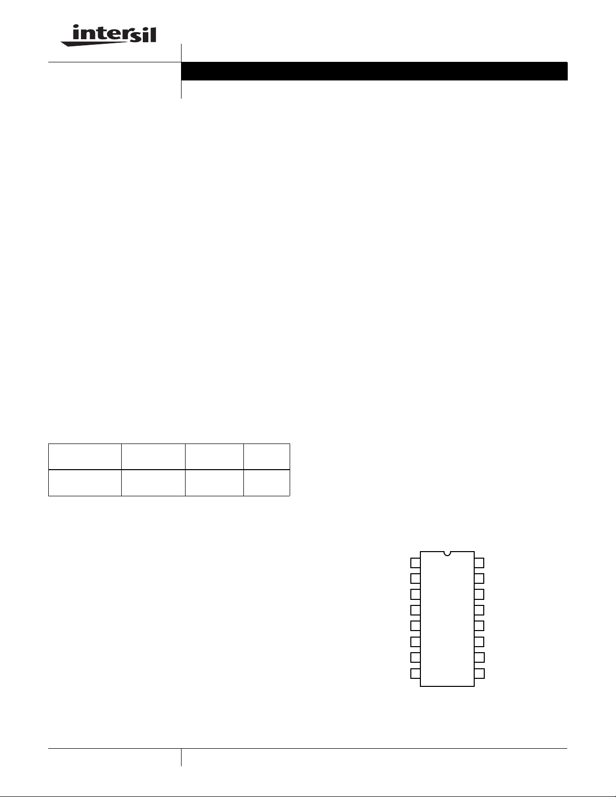
Pinout
ISL6740A (TSSOP)
TOP VIEW
OUTA
SCSET
SYNC
V
ERROR
UV/FF
GND
C
CS
1
2
3
4
T
5
6
7
8
16
15
14
13
12
11
10
9
OUTB
V
REF
V
DD
R
TD
R
TC
OTS
FAULT
SS
1
CAUTION: These devices are sensitive to electrostatic discharge; follow proper IC Handling Procedures.
1-888-INTERSIL or 1-888-352-6832
| Intersil (and design) is a registered trademark of Intersil Americas Inc.
All other trademarks mentioned are the property of their respective owners.
Copyright Intersil Americas Inc. 2005. All Rights Reserved
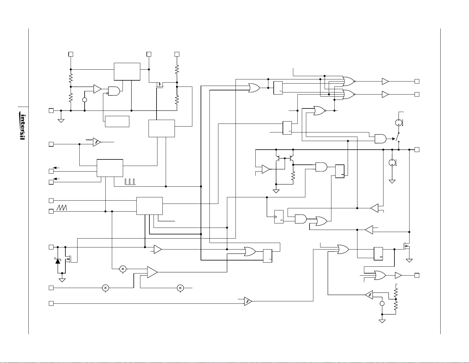
Functional Block Diagram
www.BDTIC.com/Intersil
V
DD
V
REF
5.00 V
1%
ENABLE
+
-
2
GND
UV/FF
I
R
R
SCSET
CS
V
ERROR
February 7, 2005
OTS
RTC
TC
I
RTD
TD
C
T
BG
1.00 V
+
-
INHIBIT/VIN UV
+
-
Internal
OT Shutdown
130 - 150 C
Oscillator
0.4
INHIBIT
CLK
0.4
V
REF
N_SYNC OUT
EXT. SYNC
Short Circuit
Detection
0.6 V
+
-
-
100
4.5 k
Bi-Directional
Synchronization
OC DETECT
+
-
PWM
COMPARAT OR
SYNC
SYNC IN
SS DONE
0.5
FL
V
REF
70µA
OUTA
OUTB
SS
ISL6740A
FAULT
Q
T
Q
PWM TOGGLE
SC S/D
SRQ
SS LOW
-
+
4.5 V
SS CLAMP
RETRIGGERABLE
ONE SHOT
SRQ
Q
PWM LATCH
RESET
DOMINANT
SS
-
V
/2
REF
+
Q
SC LATCH
SS DONE
300 k
Q
Q
50 µS
INHIBIT
OC S/D
OC LATCH
SRQ
Q
V
REF
SC S/D
UV 4.65 V
SS HI
OC S/D
+
-
4.25 V
0.27 VSS LOW
+
-
FAULT LATCH
SET DOMINANT
SRQ
FL
Q
-
+
+
BG
-
ON
15µA
V
REF
FN9195.0
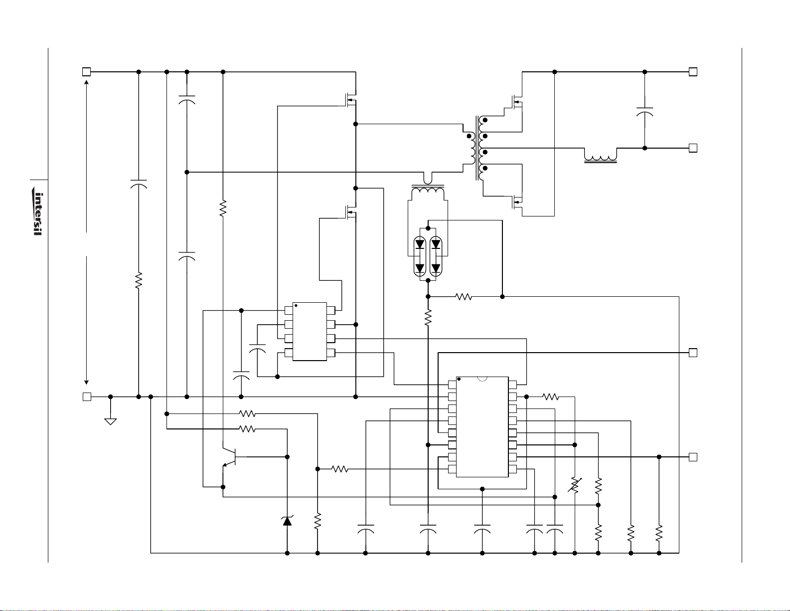
Typical Application - 48V Input Bus Converter, 9V @ 10A Output
www.BDTIC.com/Intersil
VIN+
Q1
C2
3
36-75V
VIN-
February 7, 2005
C1
R2
R1
C3
1
VDD
HB
2
HO
3
HS
4 5
C5
C4
R3
R4
Q3
VR1
Q2
U1
LO
8
HIP2101
7
VSS
LI
6
HI
R5
R6
T2
CR1
R13
T1
CR2
R12
U3
1
OUTA
GND
2
3
SCSET
4
CT
5
SYNC
6
CS
7
VERROR
89
UV/FF SS
OUTB
VREF
VDD
ISL6740A
RTD
RTC
OTS
FAULT
FN9195.0
C6
C8
QR1
C11
L1
QR2
16
15
14
13
12
11
10
R11
R8
RT1
R10
C9C7
C10
R7
R9
+9V
RTN
ISL6740A
SYNC
FAULT
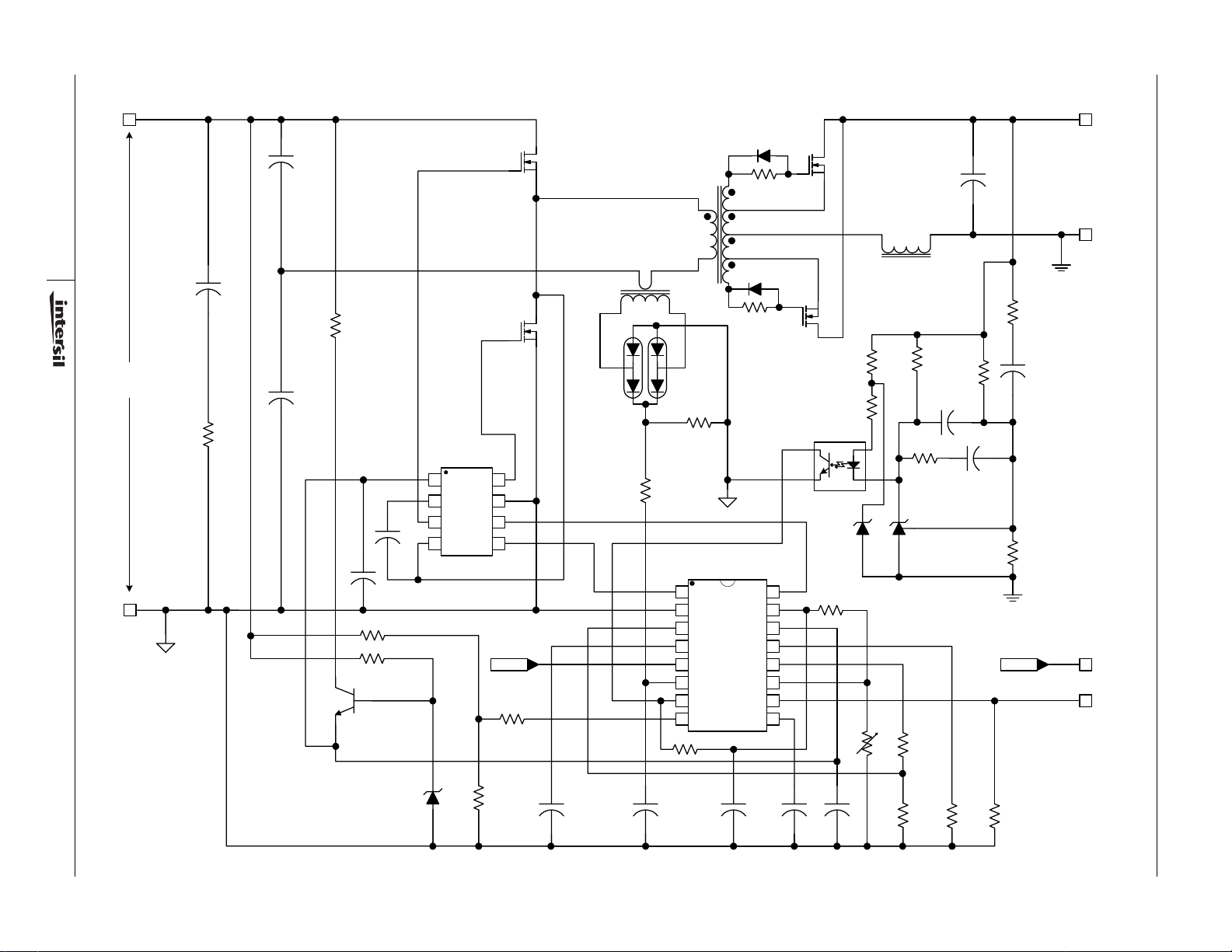
Typical Application - 36 to 75 V Input, Regulated 12V @ 8A Output
www.BDTIC.com/Intersil
VIN+
CR3
Q1
C2
T1
R22
QR1
C11
L1
+12V
RTN
4
C1
U1
HIP2101
VSS
Q2
8
LO
7
6
LI
HI
R5
R6
R2
36-75V
R1
VIN-
February 7, 2005
C3
1
VDD
HB
2
HO
3
4 5
C5
C4
R3
R4
Q3
VR1
HS
FN9195.0
T2
CR1
R13
C6 C9C7
CR2
R14
1
OUTA
2
GND
3
SCSET
4
CT
5
SYNC
6
CS
7
VERROR
89
UV/FF SS
R7
U2
ISL6740A
FAULT
CR4
R23
OUTB
VREF
VDD
RTD
RTC
OTS
C8
QR2
R17
R18
R19
R20
C13
R21
C12
ISL6740A
R16
U3
2801-1
VR2
16
15
14
13
12
11
10
R12
C10
RT1
U4
TL431
R8
R9
C14
R10
R15
R11
SYNCSYNC
SYNC I/O
FAULT
ISL6740A
www.BDTIC.com/Intersil
Absolute Maximum Ratings Thermal Information
Supply Voltage, VDD . . . . . . . . . . . . . . . . . . . GND - 0.3V to +20.0V
OUTA, OUTB, Signal Pins . . . . . . . . . . . . . . . . .GND - 0.3V to V
VREF . . . . . . . . . . . . . . . . . . . . . . . . . . . . . . . . . GND - 0.3V to 6.0V
Peak GATE Current . . . . . . . . . . . . . . . . . . . . . . . . . . . . . . . . . . 0.5A
ESD Classification
Human Body Model (Per MIL-STD-883 Method 3015.7) . . .1500V
Charged Device Model (Per EOS/ESD DS5.3, 4/14/93) . . .1000V
REF
Thermal Resistance Junction to Ambient (Typical) θ
16 Lead TSSOP (Note 1) . . . . . . . . . . . . . . . . . . . 102
Maximum Junction Temperature . . . . . . . . . . . . . . . . -55°C to 150°C
Maximum Storage Temperature Range. . . . . . . . . . . -65°C to 150°C
Maximum Lead Temperature (Soldering 10s) . . . . . . . . . . . . . 300°C
(TSSOP- Lead Tips Only)
Operating Conditions
Temperature Range
ISL6740AIVx. . . . . . . . . . . . . . . . . . . . . . . . . . . .-40°C to 105°C
Supply Voltage Range (Typical). . . . . . . . . . . . . . . . . 9VDC-16 VDC
CAUTION: Stresses above those listed in “Absolute Maximum Ratings” may cause permanent damage to the device. This is a stress only rating and operation of the
device at these or any other conditions above those indicated in the operational sections of this specification is not implied.
NOTES:
is measured with the component mounted on a high effective thermal conductivity test board in free air. See Tech Brief TB379 for details.
1. θ
JA
2. All voltages are with respect to GND.
Electrical Specifications Recommended operating conditions unless otherwise noted. Refer to Block Diagram and Typical Application
Schematic. 9V < V
values are at T
PARAMETER TEST CONDITIONS MIN TYP MAX UNITS
SUPPLY VOLTAGE
Start-Up Current, I
Operating Current, I
UVLO START Threshold 6.50 7.25 8.00 V
UVLO STOP Threshold 6.00 6.75 7.50 V
Hysteresis 0.35 0.50 0.75 V
REFERENCE VOLTAGE
Overall Accuracy I
Long Term Stability T
Fault Voltage 4.10 4.55 4.75 V
VREF Good Voltage 4.25 4.75 V
Hysteresis 75 165 250 mV
Operational Current (source) -20 - - mA
Operational Current (sink) 5--mA
Current Limit -25 - -100 mA
CURRENT SENSE
Current Limit Threshold V
CS to OUT Delay -3550ns
CS Sink Current -10-mA
Input Bias Current -1.00 - 1.00 µA
SCSET Input Impedance 1- -MΩ
SC Setpoint Accuracy -10-%
PULSE WIDTH MODULATOR
V
Input Impedance 400 - - kΩ
ERROR
DD
DD
< 20 V, RTD = 51.1kΩ, R
DD
= 25°C
A
V
< START Threshold - 95 140 µA
DD
R
, C
LOAD
C
OUTA,B
= 0, -20mA 4.900 5.000 5.050 V
VREF
= 125°C, 1000 hours (Note 4) - 3 - mV
A
= V
ERROR
= 0 - 5.0 8.0 mA
OUTA,B
= 1nF - 7.0 12.0 mA
REF
= 10kΩ, CT = 470pF, TA = -40°C to 105°C (Note 3), Typical
TC
REF
-.05
0.55 0.6 0.65 V
(°C/W)
JA
V
5
FN9195.0
February 7, 2005

ISL6740A
www.BDTIC.com/Intersil
Electrical Specifications Recommended operating conditions unless otherwise noted. Refer to Block Diagram and Typical Application
Schematic. 9V < V
values are at T
PARAMETER TEST CONDITIONS MIN TYP MAX UNITS
Minimum Duty Cycle V
Maximum Duty Cycle V
V
C
SS to PWM Comparator Input Gain (Note 4) - 0.5 - V/V
OSCILLATOR
Frequency Accuracy T
Frequency Variation with V
Frequency Variation with V
Temperature Stability V
Charge Current Gain 1.88 2.0 2.12 µA/µA
Discharge Current Gain 45 55 65 µA/µA
C
C
C
SYNCHRONIZATION
Input High Threshold (VIH), Minimum 4.0 - - V
Input Low Threshold (VIL), Maximum --0.8V
Input Impedance -4.5-kΩ
Input Frequency Range (Note 4) 0.6x
Input Pulse Width (Note 4) 100 - - ns
High Level Output Voltage (VOH) I
Low Level Output Voltage (VOL) I
SYNC Output Current VOH > 2.0V (Note 4) -10 - - mA
SYNC Output Pulse Duration (minimum) (Notes 4, 5) 250 - 400 ns
SYNC Advance SYNC rising edge to GATE falling edge,
to PWM Comparator Input Gain (Note 4) - 0.4 - V/V
ERROR
to PWM Comparator Input Gain (Note 4) - 0.4 - V/V
T
DD
UV/FF
Valley Voltage Static operation 0.75 0.80 0.85 V
T
Peak Voltage Static operation
T
Peak Voltage Static operation
T
< 20 V, RTD = 51.1kΩ, R
DD
= 25°C (Continued)
A
< CT Valley Voltage - - 0 %
ERROR
> 4.75V, V
ERROR
R
= 5.11kΩ, RTC = 25.5kΩ, CT = 220pF
TD
= 25°C (Note 7) 333 351 369 kHz
A
TA = 105°C, |(F
(Note 4)
= 25°C, |(F
T
A
= -40°C, |(F
T
A
(Note 4)
TA = 25°C, |(F
V
= 9V - 1.2 3 %
DD
= 20V - 1.2 3 %
V
DD
= 2.0V, VDD = 9V (Note 4) - 0.5 1.5 %
UV/FF
= 2.00V 2.30 2.40 2.50 V
V
UV/FF
= 4.25V 4.10 4.20 4.30 V
V
UV/FF
V
= 2.00V 2.30 2.40 2.50 V
UV/FF
= 4.25V 4.10 4.20 4.30 V
V
UV/FF
= -1mA - 4.5 - V
LOAD
= 10µA - - 100 mV
LOAD
OUTA/B
= C
C
(Note 4)
UV/FF
- F9V)/F9V|, UV/FF = 2.00V
20V
- F9V)/F9V|, UV/FF = 2.00V - 0.1 0.3
20V
- F9V)/F9V|, UV/FF = 2.00V
20V
- F
4.25V
= 100pF
SYNC
= 10kΩ, CT = 470pF, TA = -40°C to 105°C (Note 3), Typical
TC
= 2.5V (Note 6)
)/F
2.00V
2.00V
| %
-83-%
-99-%
-0.10.4%
-0.20.7
Free
Running
-5-ns
- Free
Running
Hz
6
FN9195.0
February 7, 2005

ISL6740A
www.BDTIC.com/Intersil
Electrical Specifications Recommended operating conditions unless otherwise noted. Refer to Block Diagram and Typical Application
Schematic. 9V < V
values are at T
PARAMETER TEST CONDITIONS MIN TYP MAX UNITS
SOFT-START
Charging Current SS = 2V -45 -55 -75 µA
SS Clamp Voltage 4.35 4.5 4.65 V
Sustained Overcurrent Threshold Voltage Charged Threshold minus: 0.20 0.25 0.30 V
Overcurrent/Short Circuit Discharge Current SS = 2V 13 18 23 µA
Fault SS Discharge Current SS = 2V - 10.0 - mA
Reset Threshold Voltage 0.25 0.27 0.33 V
FAULT
Fault High Level Output Voltage (VOH) I
Fault Low Level Output Voltage (VOL) I
Fault Rise Time C
Fault Fall Time C
OUTPUT
High Level Output Voltage (VOH) V
Low Level Output Voltage (VOL) OUTA or OUTB - GND, I
Rise Time C
Fall Time C
THERMAL PROTECTION
Thermal Shutdown (Note 4) 135 145 155 °C
Thermal Shutdown Clear (Note 4) 120 130 140 °C
Hysteresis, Internal Protection (Note 4) - 15 - °C
OTS
Threshold 2.375 2.50 2.625 V
Hysteresis, Switched Current Amplitude 18 25 30 µA
UV/FF Undervoltage Inhibit/Feed Forward
Input Voltage Low/Inhibit Threshold 0.97 1.00 1.03 V
Hysteresis, Switched Current Amplitude 7 10 15 µA
Input High Clamp Voltage 4.8 - - V
Input Impedance 1--MΩ
FF Gain V
Maximum Control Voltage 4.20 - V
NOTES:
3. Specifications at -40°C and 105°C are guaranteed by 25°C test with margin limits.
4. Guaranteed by design, not 100% tested in production.
5. SYNC pulse width is the greater of this value or the C
6. This is the maximum duty cycle achievable using the specified values of R
obtained using other values for these components. See Equations 2-4.
7. The oscillator frequency is affected by the tolerance of the timing components used. In particular, parasitic capacitance at the CT pin introduced
by layout, leads, and probes, etc. will lower the frequency.
< 20 V, RTD = 51.1kΩ, R
DD
= 25°C (Continued)
A
= -10mA 2.85 3.5 - V
LOAD
= 10mA - 0.4 0.9 V
LOAD
= 100pF (Note 4) - 15 - ns
LOAD
= 100pF (Note 4) - 15 - ns
LOAD
- OUTA or OUTB,
REF
= -50mA, 1µS duration, C
I
OUT
1µs duration, C
= 1nF, VDD = 15V (Note 4) - 50 100 ns
GATE
= 1nF, VDD = 15V (Note 4) - 40 80 ns
GATE
, V
RTD/VFF
discharge time.
T
RTC/VFF
VREF
= 1.0µF
= 10kΩ, CT = 470pF, TA = -40°C to 105°C (Note 3), Typical
TC
-0.51.0V
= 1.0µF
VREF
= 50mA,
OUT
, RTD, and CT. Larger or smaller maximum duty cycles may be
TC
-0.51.0V
0.78 0.8 0.82 V/V
REF
V
7
FN9195.0
February 7, 2005
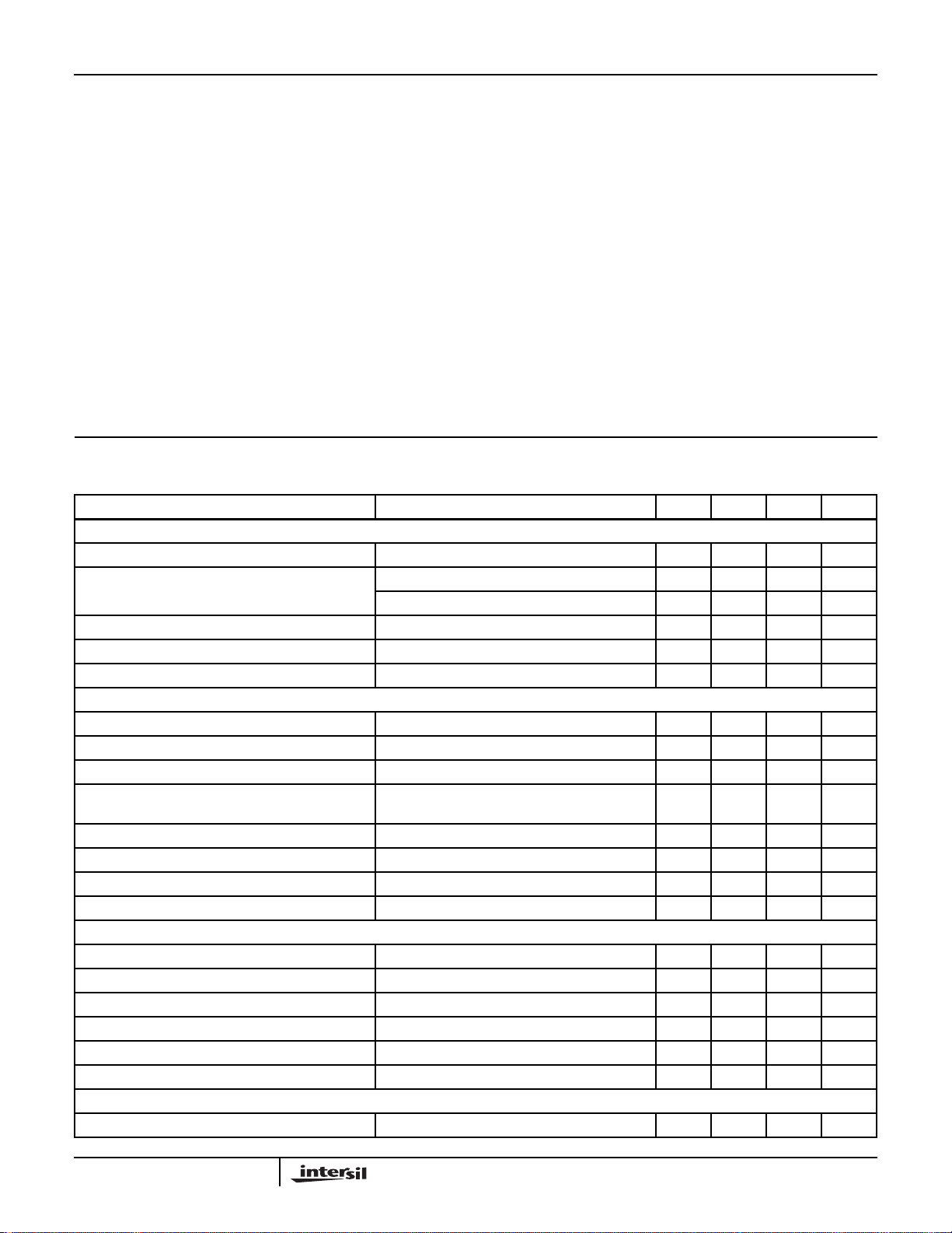
Typical Performance Curves
www.BDTIC.com/Intersil
ISL6740A
1.001
1
REF
0.999
0.998
NORMALIZED V
0.997
-40 -25 -10 5 20 35 50 65 80 95 110
TEMPERATURE (°C)
FIGURE 1. REFERENCE VOLTAGE vs TEMPERATURE FIGURE 2. OSCILLATOR CT DISCHARGE CURRENT GAIN
4
1•10
CT (pF) =
1000
680
470
330
3
1•10
220
100
100
DEADTIME - TD (ns)
10
10 20 30 40 50 60 70 80 90 100
RTD (kΩ)
65
60
55
50
45
CT DISCHARGE CURRENT GAIN
40
0 50 100 150 200 250 300 350 400 450 500
RTD CURRENT (µA)
6
1•10
5
1•10
RTD = 10K
FREQUENCY (Hz)
CT (pF) =
100
220
330
470
4
1•10
10 20 30 40 50
680
1000
60 70 80 90 100
RTC (kΩ)
FIGURE 3. DEADTIME (DT) vs CAPACITANCE FIGURE 4. CAPACITANCE vs FREQUENCY
Pin Descriptions
VDD - VDD is the power connection for the IC. To optimize
noise immunity, bypass V
capacitor as close to the V
The total supply current, I
applied to outputs OUTA and OUTB. Total I
sum of the quiescent current and the average output current.
Knowing the operating frequency, Fsw, and the output
loading capacitance charge, Q, per output, the average
output current can be calculated from:
I
2QFSW••= A
OUT
SYNC - A bidirectional synchronization signal used to
coordinate the switching frequency of multiple units.
Synchronization may be achieved by connecting the SYNC
signal of each unit together or by using an external master
clock signal. The oscillator timing capacitor, C
required regardless of the synchronization method used.
The paralleled unit with the highest oscillator frequency
assumes control.
to GND with a ceramic
DD
and GND pins as possible.
DD
, will be dependent on the load
DD
current is the
DD
, is always
T
(EQ. 1)
R
- This is the oscillator timing capacitor charge current
TC
control pin. A resistor is connected between this pin and
GND. The current flowing through the resistor determines
the magnitude of the charge current. The charge current is
nominally twice this current. The PWM maximum ON time is
determined by the timing capacitor charge duration. The
voltage appearing on this pin is nominally 80% of the voltage
applied to the UV/FF pin.
R
- This is the oscillator timing capacitor discharge current
TD
control pin. A resistor is connected between this pin and
GND. The current flowing through the resistor determines
the magnitude of the discharge current. The discharge
current is nominally 50x this current. The PWM deadtime is
determined by the timing capacitor discharge duration. The
voltage appearing on this pin is nominally 80% of the voltage
applied to the UV/FF pin.
C
- The oscillator timing capacitor is connected between
T
this pin and GND.
8
FN9195.0
February 7, 2005

ISL6740A
www.BDTIC.com/Intersil
V
error voltage is applied to this pin to control the duty cycle.
Increasing the signal level increases the duty cycle. The
node may be driven with an external error amplifier or optocoupler.
The ISL6740A features a built-in soft-start capability. Softstart is implemented as a clamp on the error voltage input.
OTS - The non-inverting input to the over temperature
shutdown comparator. The signal input at this pin is
compared to an internal threshold of V
this pin exceeds the threshold, the Fault signal is asserted
and the outputs are disabled until the condition clears. There
is a nominal 25µA switched current source used for
hysteresis. The amount of hysteresis is adjustable by
varying the source impedance of the signal into this pin.
OTS may be used to monitor parameters other than
temperature, such as voltage. Any signal for which a high
out-of-bounds monitor is desired may utilize the OTS
comparator.
FAULT - The Fault signal is asserted high whenever the
outputs, OUTA and OUTB, are disabled. This occurs during
an over temperature fault, an input UV fault, a V
fault, or during an overcurrent or short circuit shutdown fault.
Fault can be used to disable synchronous rectifiers
whenever the outputs are disabled.
Fault is a three-state output and is high impedance during
the soft-start cycle. Adding a pull-up resistor to VREF or a
pull-down resistor to ground determines the state of Fault
during soft-start. This feature allows the designer to use the
Fault signal to enable or disable output synchronous
rectifiers during soft-start.
UV/FF - Undervoltage monitor and voltage feed forward
input pin. A resistor divider between the input source voltage
and GND sets the undervoltage lock-out threshold and
provides voltage sensing for the feed forward compensation
circuit.
The signal is compared to an internal 1.00V reference to
detect an undervoltage or inhibit condition. For voltages in
excess of the UV threshold, the signal provides voltage
information to the voltage feed forward function.
CS - This is the input to the current sense comparator. The
overcurrent comparator threshold is set at 0.600V nominal.
The CS pin is shorted to GND at the termination of each
output pulse. Depending on the current sensing source
impedance, a series input resistor may be required due to
the delay between the internal clock and the external power
switch. This delay may allow an overlap such that the CS
signal may be discharged while the current signal is still
active. If the current sense source is low impedance it will
cause increased power dissipation.
- The inverting input of the PWM comparator. The
ERROR
/2. If the voltage at
REF
REF
UV
Exceeding the overcurrent threshold will start a delayed
shutdown sequence. Once an overcurrent condition is
detected, the soft-start charge current source is disabled.
The soft-start capacitor begins discharging through a 25µA
current source, and if it discharges to less than 4.25V
(Sustained Overcurrent Threshold), a shutdown condition
occurs and the OUTA and OUTB outputs are forced low.
When the soft-start voltage reaches 0.27V (Reset
Threshold) a soft-start cycle begins.
An overcurrent condition must be absent for 50µs before the
delayed shutdown control resets. If the overcurrent condition
ceases, and an additional 50µs period elapses before the
shutdown threshold is reached, no shutdown occurs. The SS
charging current is re-enabled and the soft-start voltage is
allowed to recover.
GND - Reference and power ground for all functions on this
device. Due to high peak currents and high frequency
operation, a low impedance layout is necessary. Ground
planes and short traces are highly recommended.
OUTA and OUTB - Alternate half cycle output stages. Each
output is capable of 0.5A peak currents for driving logic level
power MOSFETs or MOSFET drivers. Each output provides
very low impedance to overshoot and undershoot.
VREF - The 5.00V reference voltage output. +1/-2%
tolerance over line, load and operating temperature. Bypass
to GND with a 0.047µF to 2.2µF ceramic capacitor.
Capacitors outside of this range may cause oscillation.
SS - Connect the soft-start timing capacitor between this pin
and GND to control the duration of soft-start. The value of
the capacitor determines the rate of increase of the duty
cycle during start up, controls the overcurrent shutdown
delay, and the overcurrent and short circuit hiccup restart
period.
SCSET - Sets the duty cycle threshold that corresponds to a
short circuit condition. A resistive divider between R
GND, V
and 2V may be used to adjust the SCSET threshold. If using
a resistor divider from either RTC or RTD, the impedance to
GND affects the oscillator timing and should be considered
when determining the oscillator timing components.
Connecting SCSET to GND disables short circuit shutdown
and hiccup.
to GND, RTD and GND, or a voltage between 0
REF
TC
and
Functional Description
Features
The ISL6740A PWM is an excellent choice for low cost feed
forward voltage mode bridge topologies for applications
requiring accurate duty cycle and deadtime control. With its
many protection and control features, a highly flexible design
with minimal external components is possible. Among its
many features are voltage feed forward compensation,
adjustable soft-start, overcurrent protection, thermal
9
FN9195.0
February 7, 2005

ISL6740A
www.BDTIC.com/Intersil
protection, bidirectional synchronization, fault indication, and
adjustable frequency.
Oscillator
The ISL6740A has an oscillator with a programmable
frequency range to 2MHz, and can be programmed with two
resistors and a capacitor. The use of three timing elements,
R
, RTD, and CT allows great flexibility and precision when
TC
setting the oscillator frequency.
The switching period is the sum of the timing capacitor
charge and discharge durations. The charge duration is
determined by R
determined by R
TC0.5 RTC• CT•≈ S
T
0.02 RTD• CT•≈ S
D
T
SWTCTD
where T
+
and TD are the charge and discharge times,
C
respectively, T
and CT. The discharge duration is
TC
and CT.
TD
1
------------== S
F
SW
is the oscillator free running period, and f
SW
(EQ. 2)
(EQ. 3)
(EQ. 4)
is the oscillator frequency. One output switching cycle
requires two oscillator cycles. The actual times will be
slightly longer than calculated due to internal propagation
delays of approximately 10ns/transition. This delay ads
directly to the switching duration, but also causes overshoot
of the timing capacitor peak and valley voltage thresholds,
effectively increasing the peak-to-peak voltage on the timing
capacitor. Additionally, if very low charge and discharge
currents are used, there will be increased error due to the
input impedance at the C
T
pin.
The maximum duty cycle, D, and percent deadtime, DT, can
be calculated from:
T
C
------------=
D
T
SW
DT 1 D–= (EQ. 6)
(EQ. 5)
FIGs. 3 and 4 graphically portray the deadtime and oscillator
frequency as function of the timing components.
Implementing Synchronization
The oscillator can be synchronized to an external clock
applied to the SYNC pin or by connecting the SYNC pins of
multiple ICs together. If an external master clock signal is
used, the free running frequency of the oscillator should be
~10% slower than the desired synchronous frequency. The
external master clock signal should have a pulse width
greater than 20ns. The SYNC circuitry will not respond to an
external signal during the first 60% of the oscillator switching
cycle.
The SYNC input is edge triggered and its duration does not
affect oscillator operation. However, the deadtime is affected
by the SYNC frequency. A higher frequency signal applied to
the SYNC input will shorten the deadtime. The shortened
deadtime is the result of the timing capacitor charge cycle
being prematurely terminated by the external SYNC pulse.
Consequently, the timing capacitor is not fully charged when
the discharge cycle begins. This effect is only a concern
when an external master clock is used, or if units with
different operating frequencies are paralleled.
Soft-Start Operation
Soft-start is controlled using an external capacitor in
conjunction with an internal current source. Soft-start
reduces stresses and surge currents during start up.
Upon start up, the soft-start circuitry clamps the error voltage
input (V
pin) indirectly to a value equal to the soft-
ERROR
start voltage. The soft-start clamp does not actually clamp
the error voltage input as is done in many implementations.
Rather the PWM comparator has two inverting inputs such
that the lower voltage is in control.
The output pulse width increases as the soft-start capacitor
voltage increases. This has the effect of increasing the duty
cycle from zero to the regulation pulse width during the softstart period. When the soft-start voltage exceeds the error
voltage at the PWM comparator inputs, soft-start is
completed. Soft-start occurs during start-up, after recovery
from a Fault condition or overcurrent/short circuit shutdown.
The soft-start voltage is clamped to 4.5V.
The Fault signal output is high impedance during the softstart cycle unless an active fault (see Fault Conditions) is
present. A pull-up resistor to VREF or a pull-down resistor to
ground should be added to achieve the desired state of Fault
during soft-start.
Gate Drive
The outputs are capable of sourcing and sinking 0.5A peak
current, but are primarily intended to be used in conjunction
with a MOSFET driver due to the 5V drive level. To limit the
peak current through the IC, an external resistor may be
placed between the totem-pole output of the IC (OUTA or
OUTB pin) and the gate of the MOSFET. This small series
resistor also damps any oscillations caused by the resonant
tank formed by the parasitic inductances in the traces of the
board and the device’s input capacitance.
Undervoltage Monitor, Inhibit, and Feed Forward
The UV/FF input is used for input source undervoltage
lockout and inhibit functions as well as sensing the input
voltage for feed forward compensation.
If the node voltage falls below 1.00V, a UV shutdown fault
occurs. This may be caused by low source voltage or by
intentional grounding of the pin to disable the outputs. There
is a nominal 10µA switched current source used to create
hysteresis. The current source is active only during a
10
FN9195.0
February 7, 2005

ISL6740A
www.BDTIC.com/Intersil
UV/Inhibit fault; otherwise, it is inactive and does not affect
the node voltage. The magnitude of the hysteresis is a
function of the external resistor divider impedance. If the
resistor divider impedance results in too little hysteresis, a
series resistor between the UV pin and the divider may be
used to increase the hysteresis. A soft-start cycle begins
when the UV/Inhibit fault clears.
The voltage hysteresis created by the switched current
source and the external impedance is generally small due to
the large resistor divider ratio required to scale the input
voltage down to the UV threshold level. A small capacitor
placed between the UV input and ground may be required to
filter noise out.
V
IN
R1
+
1.00V
-
R3
R2
FIGURE 5. UV HYSTERESIS
As V
decreases to a UV condition, the threshold level is:
IN
V
IN DOWN()
R1 R2+
----------------------= V
R2
10µA
ON
(EQ. 7)
The hysteresis voltage, ∆V, is :
∆V10
5–
R1 R3
R1 R2+
----------------------
•+〈〉•= V
R2
(EQ. 8)
the oscillator. The voltage feed forward operates over a 3:1
input voltage range.
V
UV/FF
V
ERROR
CT
OUTA
OUTB
FIGURE 6. FEED FORWARD BEHAVIOR
The voltage applied to the UV/FF pin is multiplied by 0.8 and
output on the R
summed with the C
create the C
and RTD pins. This voltage is also
TC
valley threshold voltage (0.8 V) to
T
peak threshold voltage. As the voltage applied
T
to UV/FF varies, the CT peak voltage and the CT charge and
discharge currents vary, all in direct proportion to each other.
The result is an amplitude modulated sawtooth waveform on
C
that is frequency invariant.
T
The voltage amplitude of CT ranges from 1.6V to 4.2V as the
voltage on UV increases. The UV threshold defines the
minimum amplitude of C
and corresponds to maximum duty
T
cycle operation.
For unregulated bus converters and DC transformers, feed
forward can compensate for input voltage variations without
a closed loop feedback network. A resistive voltage divider
from V
REF
to V
sets the feed forward control voltage.
ERROR
For example, if the desired duty cycle at the minimum
operating voltage is 90%, then
V
ERRORDmaxVUV FF⁄
0.9 1.0 0.8•()0.8+ 1.52== V
0.8•()0.8+= V
(EQ. 11)
Setting R3 equal to zero results in the minimum hysteresis,
and yields:
5–
∆V10
R1•= V
(EQ. 9)
Overcurrent Protection
There are two overcurrent protection mechanisms in the
ISL6740A, one for light overcurrent and one for heavy over
load. They are referred to, respectively, as overcurrent
protection and short circuit protection.
As V
increases from a UV condition, the threshold level is:
IN
V
IN UP()VIN DOWN()
∆V+= V
(EQ. 10)
Overcurrent Operation
Overcurrent delayed shutdown is enabled once the soft-start
cycle is complete. If an overcurrent condition is detected, the
Output voltage variation caused by changes in the supply
voltage may be virtually removed through a technique known
as feed forward compensation. Using feed forward, the duty
cycle is directly modulated based on changes in the input
voltage only. No closed loop feedback system is required.
The feed forward circuit uses the voltage applied to the
UV/FF pin to modulate the oscillator ramp amplitude with
minimal effect on the switching frequency and deadtime of
soft-start charging current source is disabled and the softstart capacitor is allowed to discharge through a 15µA
source. At the same time a 50µs re-triggerable one-shot
timer is activated. It remains active for 50µs after the
overcurrent condition ceases. If the soft-start capacitor
discharges by more then 0.25V to 4.25V, the output is
disabled and the Fault signal asserted. This state continues
until the soft-start voltage reaches 270mV, at which time a
new soft-start cycle is initiated. If the overcurrent condition
11
FN9195.0
February 7, 2005

ISL6740A
www.BDTIC.com/Intersil
stops at least 50µs prior to the soft-start voltage decreasing
to 4.25V, the soft-start charging currents revert to normal
operation and the soft-start voltage is allowed to recover.
4.5 V
SS
0.6 V OC
CS
OUTA
OUTB
FIGURE 7. PULSE-BY-PULSE OC BEHAVIOR DURING SS
Figure 7 shows the overcurrent behavior during SS.
Although an overcurrent condition exists, a shutdown is not
allowed prior to completion of the SS cycle. Only peak
current limit operates during the soft-start cycle. If the
overcurrent condition were to continue beyond the soft-start
cycle, a delayed overcurrent shutdown would occur as
shown in Figure 8.
SS
4.5 V
If the overcurrent condition is removed prior to a shutdown, a
recovery can occur as indicated in Figure 9. When the load
decreases below the overcurrent threshold and an additional
50µs elapses without the SS dropping below 4.25V, the
overcurrent circuitry resets and the soft-start voltage
recovers.
The duration of the OC shutdown period can be increased
by adding a resistor between VREF and SS. The value of
the resistor must be large enough so that the minimum
specified SS discharge current is not exceeded. Using a
422kΩ resistor, for example, will result in a small current
being injected into SS, effectively reducing the discharge
current. This will nearly double the OFF time. The external
pull-up resistor will also decrease the SS duration, so its
effect should be considered when selecting the value of the
SS capacitor.
1
2
3
4
ISL6740A
5
6
7
89
VREF
16
15
14
13
12
R
11
10
SS
4.25 V
0.27 V
0.6 V OC
CS
OUTA
OUTB
FIGURE 8. OC SHUTDOWN BEHAVIOR
Figure 8 portrays the typical delayed overcurrent shutdown
behavior. Once SS has discharged to 4.25V, the outputs are
disabled and remain that way until SS has discharged to
0.27V, and then a new SS cycle begins.
OC
4.5 V
50 µS
SS
4.25 V
0.6 V OC
CS
OUTA
OUTB
FIGURE 9. OC RECOVERY PRIOR TO SHUTDOWN
C
SS
FIGURE 10. MODIFYING OC SHUTDOWN TIMING
Latching OC shutdown is also possible by using a lower
valued resistor between VREF and SS. If the SS node is not
allowed to discharge below the SS reset threshold, the IC
will not recover from an overcurrent fault. The value of the
resistor must be low enough so that the maximum specified
discharge current is not sufficient to pull SS below 0.33V. A
200kΩ resistor, for example, prevents SS from discharging
below ~0.4V. Again, the external pull-up resistor will
decrease the SS duration, so its effect should be considered
when selecting the value of the SS capacitor
Short Circuit Operation
If the output current increases beyond the overcurrent
threshold, peak current limit will reduce the duty cycle. As
the load current continues to increase, the duty cycle
continues to decrease. A short circuit event is defined as the
simultaneous occurrence of current limit and a reduced duty
cycle.
The degree of reduced duty cycle that defines a short circuit
condition is user adjustable using the SCSET input. A
resistor divider between R
, RTC, or V
TD
and GND to
REF
RCSET sets a threshold that is compared to the voltage on
the timing capacitor, C
. The resistor divider voltage divided
T
12
FN9195.0
February 7, 2005

ISL6740A
www.BDTIC.com/Intersil
by 2 corresponds to the duty cycle below which a short
circuit can exist.
V
D
SC
where D
⋅=
D
max
2
is the maximum short circuit duty cycle, V
SC
SCSET
-----------------------
is the voltage applied to SCSET, and D
is the maximum
max
(EQ. 12)
SCSET
duty cycle. If the timing capacitor voltage fails to exceed the
threshold before an overcurrent pulse is detected, a short
circuit condition exists. A shutdown will occur if 8 short circuit
events occur within 32 oscillator cycles. Once shutdown
occurs, SS will discharge through a 15µA current source. A
new soft-start cycle will begin when SS reaches 0.27V.
Latching shutdown may be implemented in the same
manner as described in the overcurrent section. Short circuit
shutdown is enabled once the soft-start cycle is complete.
Connecting SCSET to GND inhibits short circuit shutdown.
If either R
ar RTD are used as the voltage source for the
TC
divider, the effect of the SCSET divider must be included in
the timing calculations since the current sourced from R
and R
determine the charge and discharge currents for
TD
TC
the timing capacitor. Typically the resistor between either
R
TC
or R
and GND is formed by two series resistors with
TD
the center node connected to SCSET.
Alternatively, SCSET may be set using a voltage between
0V and 2V. This voltage divided by 2 determines the
percentage of the maximum duty cycle that corresponds to a
short circuit when current limit is active. For example, if the
maximum duty cycle is 95% and 1V is applied to SCSET,
then the short circuit duty cycle is 50% of 95% or 47.5%.
Thermal Protection
Two methods of over temperature protection are provided.
The first method is an on board temperature sensor that
protects the device should the junction temperature exceed
145°C. There is approximately 15°C of hysteresis.
The second method uses an internal comparator with a 2.5V
reference (V
/2). The non-inverting input to the
REF
comparator is accessible through the OTS pin. A thermistor
or thermal sensor located at or near the area of interest may
be connected to this input. There is a nominal 25µA switched
current source used to create hysteresis. The current source
is active only during an OT fault; otherwise, it is inactive and
does not affect the node voltage. The magnitude of the
hysteresis is a function of the external resistor divider
impedance. Either a positive temperature coefficient (PTC)
or a negative temperature coefficient (NTC) thermistor may
be used. If a NTC thermistor is desired, position R1 may be
substituted. If a PTC is desired, then position R2 may be
V
V
REF
R1
R3
R2
REF
25µA
V
REF
ON
+
-
/2
Fault Conditions
A fault condition occurs if any of the following conditions
occur:
•V
• UV falls below 1.00V
• the internal thermal protection triggers
•OTS faults
When any of the above faults are detected, OUTA and
OUTB outputs are disabled, Fault is asserted, and the softstart capacitor is quickly discharged. When the fault
condition clears and the soft-start voltage is below the reset
threshold, a soft-start cycle begins. Fault is high impedance
during the soft-start cycle unless an active fault is present.
A shutdown resulting from an overcurrent or short circuit
condition also causes assertion of Fault, but the soft-start
capacitor is not quickly discharged. The initiation of a new
soft-start cycle is delayed while the soft-start capacitor is
discharged at a 15µA rate. This reduces the repetition rate of
the hiccup behavior and keeps the average output current to
a minimum.
falls below 4.65V
REF
FIGURE 11. OTS HYSTERESIS
substituted. The threshold with increasing temperature is set
by making the fixed resistance equal in value to the
thermistor resistance at the desired trip temperature.
V
↑ = 2.5V and R1 = R2 (HOT)
TH
To determine the value of the hysteresis resistor, R3, select
the value of thermistor resistance that corresponds to the
desired reset temperature.
5
R1 R2–()• R1 R2•–
10
------------------------------------------------------------ ----------
R3
R1 R2+
Ω= (EQ. 13)
13
FN9195.0
February 7, 2005

If the hysteresis resistor, R3, is not desired, the value of the
www.BDTIC.com/Intersil
thermistor resistance at the reset temperature can be
determined from:
ISL6740A
R1
R2
Other Uses for OTS
The OTS comparator may also be used to monitor signals
other than as suggested above. It may also be used to
monitor any voltage signal for which an excess requires a
response as described above. Input and output voltage
monitoring are examples of this.
2.5 R 2•
----------------------------------------= Ω NTC()
2.5 10
-----------------------------------------= Ω PTC()
2.5 10
2.5 R1•
5–
R2•–
5–
R1•+
(EQ. 14)
(EQ. 15)
Ground Plane Requirements
Careful layout is essential for satisfactory operation of the
device. A good ground plane must be employed. V
V
should be bypassed directly to GND with good high
REF
frequency capacitance.
DD
and
14
FN9195.0
February 7, 2005
ISL6740A
www.BDTIC.com/Intersil
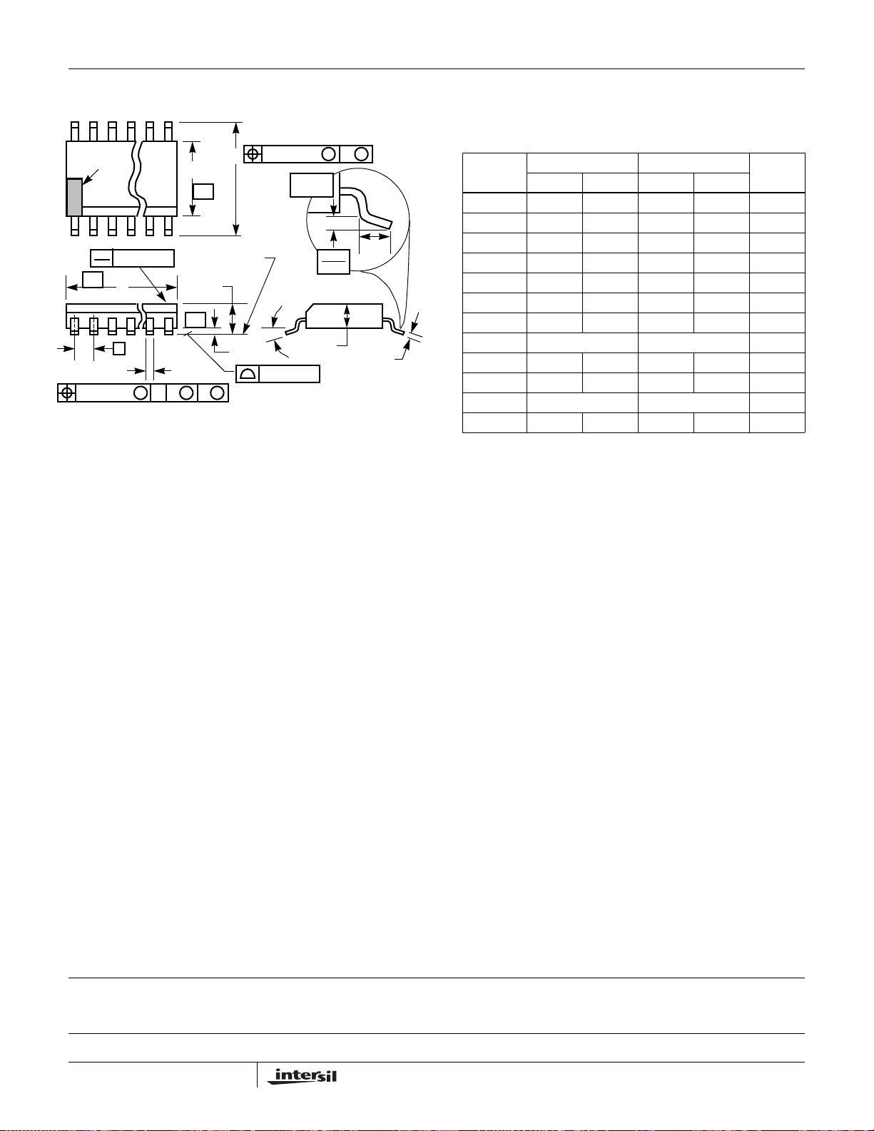
Thin Shrink Small Outline Plastic Packages (TSSOP)
N
INDEX
AREA
123
0.05(0.002)
-AD
e
b
0.10(0.004) C AM BS
NOTES:
1. These package dimensions are within allowable dimensions of
JEDEC MO-153-AB, Issue E.
2. Dimensioning and tolerancing per ANSI Y14.5M-1982.
3. Dimension “D” does not include mold flash, protrusions or gate
burrs. Mold flash, protrusion and gate burrs shall not exceed
0.15mm (0.006 inch) per side.
4. Dimension “E1” does not include interlead flash or protrusions.
Interlead flash and protrusions shall not exceed 0.15mm (0.006
inch) per side.
5. The chamfer on the body is optional. If it is not present, a visual
index feature must be located within the crosshatched area.
6. “L” is the length of terminal for soldering to a substrate.
7. “N” is the number of terminal positions.
8. Terminal numbers are shown for reference only.
9. Dimension “b” does not include dambar protrusion. Allowable
dambar protrusion shall be 0.08mm (0.003 inch) total in excess
of “b” dimension at maximum material condition. Minimum space
between protrusion and adjacent lead is 0.07mm (0.0027 inch).
10. Controlling dimension: MILLIMETER. Converted inch dimensions are not necessarily exact. (Angles in degrees)
E1
-B-
SEATING PLANE
A
-C-
M
0.25(0.010) BM M
E
α
A1
0.10(0.004)
GAUGE
PLANE
0.25
0.010
A2
M16.173
16 LEAD THIN SHRINK SMALL OUTLINE PLASTIC PACKAGE
INCHES MILLIMETERS
SYMBOL
A - 0.043 - 1.10 -
A1 0.002 0.006 0.05 0.15 -
L
c
A2 0.033 0.037 0.85 0.95 -
b 0.0075 0.012 0.19 0.30 9
c 0.0035 0.008 0.09 0.20 -
D 0.193 0.201 4.90 5.10 3
E1 0.169 0.177 4.30 4.50 4
e 0.026 BSC 0.65 BSC E 0.246 0.256 6.25 6.50 L 0.020 0.028 0.50 0.70 6
N16 167
o
α
0
o
8
o
0
o
8
NOTESMIN MAX MIN MAX
-
Rev. 1 2/02
All Intersil U.S. products are manufactured, assembled and tested utilizing ISO9000 quality systems.
Intersil Corporation’s quality certifications can be viewed at www.intersil.com/design/quality
Intersil products are sold by description only. Intersil Corporation reserves the right to make changes in circuit design, software and/or specifications at any time without
notice. Accordingly, the reader is cautioned to verify that data sheets are current before placing orders. Information furnished by Intersil is believed to be accurate and
reliable. However, no responsibility is assumed by Intersil or its subsidiaries for its use; nor for any infringements of patents or other rights of third parties which may result
from its use. No license is granted by implication or otherwise under any patent or patent rights of Intersil or its subsidiaries.
For information regarding Intersil Corporation and its products, see www.intersil.com
15
FN9195.0
February 7, 2005
 Loading...