

®
www.BDTIC.com/Intersil
ISL6729
Data Sheet December 1, 2005
Low-Cost Single-Ended Current-Mode
PWM for Microcontroller Based Power
Converters
The ISL6729 pulse width modulating (PWM) current mode
controller is designed for power conversion applications that
are based on a microcontroller or other device which can
generate a digital clock signal at the desired switching
frequency. Similar to the ISL684x family of products, the
ISL6729 provides the basic current mode PWM control
features, but eliminates the error amplifier, the oscillator, and
the reference. An external clock signal applied to the
oscillator input provides the time base and sets the
maximum duty cycle. The reduced feature set is ideal for
those applications where a microcontroller is available to
provide the monitor and control functions. The analog PWM
provides the cycle by cycle peak current mode control,
leaving the monitor and control overhead to the
microcontroller.
Ordering Information
PAR T
NUMBER
ISL6729IB ISL6729IB -40 to 105 8 Ld SOIC M8.15
ISL6729IBZ
(See Note)
ISL6729IU 6729 -40 to 105 8 Ld MSOP M8.118
ISL6729IUZ
(See Note)
Add -T to part number for Tape and Reel packaging.
NOTE: Intersil Pb-free plus anneal products employ special Pb-free
material sets; molding compounds/die attach materials and 100%
matte tin plate termination finish, which are RoHS compliant and
compatible with both SnPb and Pb-free soldering operations. Intersil
Pb-free products are MSL classified at Pb-free peak reflow
temperatures that meet or exceed the Pb-free requirements of
IPC/JEDEC J STD-020.
PAR T
MARKING
6729IBZ -40 to 105 8 Ld SOIC
6729Z -40 to 105 8 Ld MSOP
TEMP.
RANGE (°C) PACKAGE
(Pb-free)
(Pb-free)
PKG.
DWG. #
M8.15
M8.118
FN9152.2
Features
• 5V Operation
• 1A MOSFET gate driver
•400µA startup current
• 30ns propagation delay current sense to output
• Fast transient response with peak current mode control
• Switching frequency to 2MHz
• 20ns rise and fall times with 1nF output load
• Maximum Duty Cycle Determined by Clock Input Duty
Cycle
• Tight tolerance current limit threshold
• Pb-free plus anneal available (RoHS compliant)
Applications
• Telecom and Datacom Power
• Wireless Base Station Power
• File Server Power
• Industrial Power Systems
• PC Power Supplies
• Isolated Buck and Flyback Regulators
• Boost Regulators
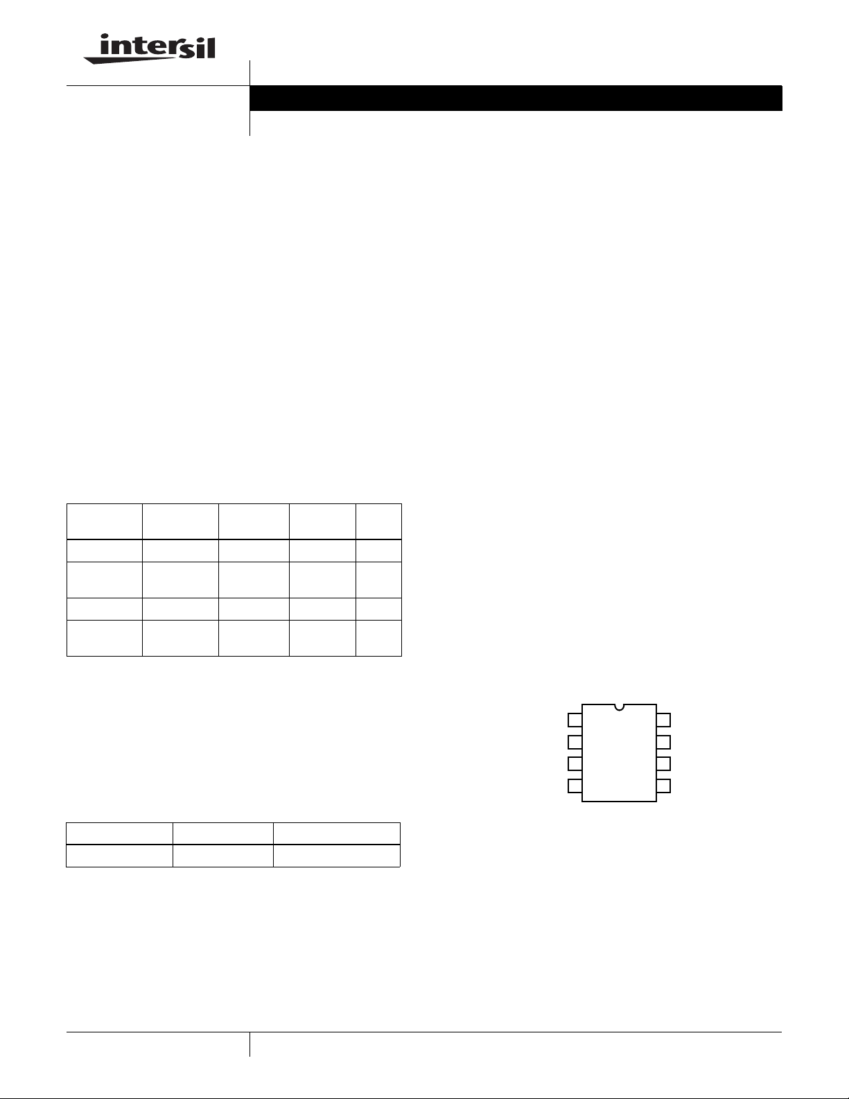
Pinout
ISL6729 (8 LD SOIC, MSOP)
TOP VIEW
COMP
N/C
CS
CLKS
1
2
3
4
8
N/C
7
VDD
6
OUT
5
GND
PART NUMBER RISING UVLO MAX. DUTY CYCLE
ISL6729 4.75V 100%
1
CAUTION: These devices are sensitive to electrostatic discharge; follow proper IC Handling Procedures.
1-888-INTERSIL or 1-888-468-3774
| Intersil (and design) is a registered trademark of Intersil Americas Inc.
Copyright © Intersil Americas Inc. 2004 - 2005. All Rights Reserved.
All other trademarks mentioned are the property of their respective owners.
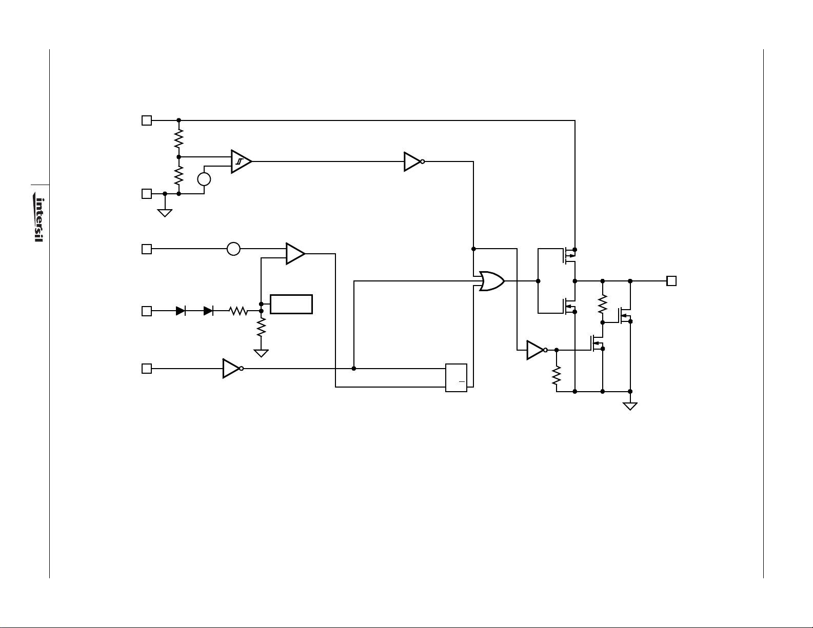
Functional Block Diagram
www.BDTIC.com/Intersil
V
DD
2
GND
START/STOP
UV COMPARATOR
+
-
BG
OK
V
+
-
DD
+
CS
COMP
CLK
December 1, 2005
-
100mV
2R
R
+
-
1.1V
CLAMP
PWM
COMPARATOR
SRQ
OUT
Q
ISL6729
FN9152.2
Typical Application - Interleaved Multi-Phase Isolated Converter
www.BDTIC.com/Intersil
VOLTAGE FEEDBACK
5V
VDD
OUT
GND
VDD
OUT
GND
VDD
OUT
GND
8
7
6
54
CURRENT FEEDBACK
8
7
6
54
CURRENT FEEDBACK
8
7
6
54
1COMP
3
CLOCK φ1
CLOCK φ2
MICROCONTROLLER
CLOCK φ3
2
3
CS
CLK
ISL6729
1COMP
2
3
CS
CLK
ISL6729
1COMP
2
3
CS
CLK
ISL6729
ISOLATION
POWER STAGE
POWER STAGE
POWER STAGE
ERROR
AMPLIFIER
VOUT
ISL6729
December 1, 2005
FN9152.2
CURRENT FEEDBACK

ISL6729
www.BDTIC.com/Intersil
Absolute Maximum Ratings Thermal Information
Supply Voltage, VDD . . . . . . . . . . . . . . . . . . . . GND - 0.3V to +6.5V
OUT . . . . . . . . . . . . . . . . . . . . . . . . . . . . .GND - 0.3V to V
Signal Pins . . . . . . . . . . . . . . . . . . . . . . . . . . . . GND - 0.3V to 6.5V
Peak GATE Current . . . . . . . . . . . . . . . . . . . . . . . . . . . . . . . . . . . .1A
ESD Classification
Human Body Model (Per MIL-STD-883 Method 3015.7) . . .2000V
Charged Device Model (Per EOS/ESD DS5.3, 4/14/93) . . .1000V
DD
+ 0.3V
Thermal Resistance (Typical, Note 1) θ
SOIC Package . . . . . . . . . . . . . . . . . . . . . . . . . . . . . 100
MSOP Package . . . . . . . . . . . . . . . . . . . . . . . . . . . . 130
Maximum Junction Temperature . . . . . . . . . . . . . . . . -55°C to 150°C
Maximum Storage Temperature Range. . . . . . . . . . . -65°C to 150°C
Maximum Lead Temperature (Soldering 10s) . . . . . . . . . . . . . 300°C
(SOIC, MSOP- Lead Tips Only)
Operating Conditions
Temperature Range
ISL6729Ix . . . . . . . . . . . . . . . . . . . . . . . . . . . . . . . .-40°C to 105°C
Supply Voltage Range (Typical)
ISL6729 . . . . . . . . . . . . . . . . . . . . . . . . . . . . . . . . . . . 4.75V-5.25V
CAUTION: Stresses above those listed in “Absolute Maximum Ratings” may cause permanent damage to the device. This is a stress only rating and operation of the
device at these or any other conditions above those indicated in the operational sections of this specification is not implied.
NOTES:
1. θ
is measured with the component mounted on a high effective thermal conductivity test board in free air. See Tech Brief TB379 for details.
JA
2. All voltages are with respect to GND.
Electrical Specifications Recommended operating conditions unless otherwise noted. Refer to Block Diagram and Typical Application
schematic. V
PARAMETER TEST CONDITIONS MIN TYP MAX UNITS
UNDERVOLTAGE LOCKOUT
START Threshold 4.15 4.50 4.75 V
STOP Threshold 4.00 4.30 4.60
Hysteresis -0.2-V
Start-Up Current, I
Operating Current, I
Operating Supply Current, I
CURRENT SENSE
Input Bias Current V
CS Offset Voltage V
COMP to PWM Comparator Offset Voltage V
CS Input Signal, Maximum 0.91 0.97 1.03 V
Gain, A
CS
CS to OUT Delay (Note 5) - 25 40 ns
CLOCK
Input High Voltage Level, VIH - 2.8 - V
Input Low Voltage Level, VIL - 2.7 - V
Maximum Clock Rate (Note 5) 2 - - MHz
OUTPUT
Gate VOH V
Gate VOL OUT - GND, I
Peak Output Current C
Rise Time C
Fall Time C
= ∆V
DD
DD
D
/∆VCS 0 < VCS < 910mV, VFB = 0V. (Note 5) 2.5 3.0 3.5 V/V
COMP
= 5V, CLK = 50kHz, TA = -40 to 105°C (Note 3), Typical values are at TA = 25°C
DD
VDD < START Threshold - 0.4 12 mA
(Note 4) - 3.3 5.5 mA
Includes 1nF GATE loading - 4.1 6.0 mA
= 1V -1.0 - 1.0 µA
CS
= 0V (Note 5) 95 100 105 mV
CS
= 0V (Note 5) 0.80 1.15 1.30 V
CS
- OUT, I
DD
= 1nF (Note 5) 1.0 - - A
OUT
= 1nF (Note 5) - 20 40 ns
OUT
= 1nF (Note 5) - 20 40 ns
OUT
= -200mA - 1.0 2.0 V
OUT
= 200mA - 1.0 2.0 V
OUT
(°C/W)
JA
4
FN9152.2
December 1, 2005

ISL6729
www.BDTIC.com/Intersil
Electrical Specifications Recommended operating conditions unless otherwise noted. Refer to Block Diagram and Typical Application
schematic. V
PARAMETER TEST CONDITIONS MIN TYP MAX UNITS
PWM
Maximum Duty Cycle -99-%
Minimum Duty Cycle --0%
NOTES:
3. Specifications at -40°C are guaranteed by design, not production tested.
4. This is the V
5. Guaranteed by design, not 100% tested in production.
current consumed when the device is active but not switching. Does not include gate drive current.
DD
Pin Descriptions
CLK - This is the oscillator timing control pin. The
operational frequency and maximum duty cycle are set by
applying a 5V amplitude clock signal to CLK. The logic high
duration defines the maximum ON time for the output. A
maximum clock rate up to 2.0MHz is possible.
COMP - COMP is the input to the PWM comparator and is
typically controlled through an external error amplifier.
CS - This is the current sense input to the PWM comparator.
The range of the input signal is nominally 0 to 1.0V and has
an internal offset of 100mV.
GND - GND is the power and small signal reference ground
for all functions.
OUT - This is the drive output to the power switching device.
It is a high current output capable of driving the gate of a
power MOSFET with peak currents of 1.0A. This GATE
output is actively held low when V
threshold.
V
- VDD is the 5V power connection for the IC. The IC will
DD
operate from 4.75V to 5.25V. However, the accuracy of the
voltage clamp on the COMP signal, which determines the
over current threshold, is dependent on the accuracy of
VDD. A tight tolerance on VDD will result in a tight over
current threshold.
The total supply current will depend on the load applied to
OU T. To t a l I
and the average output current. Knowing the operating
frequency, f, and the MOSFET gate charge, Qg, the average
output current can be calculated from:
I
OUT
To optimize noise immunity, bypass V
ceramic capacitor as close to the VDD and GND pins as
possible.
current is the sum of the operating current
DD
Qg f×=
is below the UVLO
DD
DD
= 5V, CLK = 50kHz, TA = -40 to 105°C (Note 3), Typical values are at TA = 25°C (Continued)
DD
Ground Plane Requirements
Careful layout is essential for satisfactory operation of the
device. A good ground plane must be employed. A unique
section of the ground plane must be designated for high di/dt
currents associated with the output stage. V
bypassed directly to GND with good high frequency
capacitors.
should be
DD
Applications Information
Microcontrollers are becoming more popular for monitoring
and supervisory functions in power converters due to their
flexibility, capability, and declining prices. Many applications
would like to take advantage of this flexibility and use them
to perform the control loop function as well. There are many
examples of voltage mode control using digital signal
processing techniques. However, microcontrollers available
today do not have the execution speed required for peak
current mode control at the operational frequencies of
modern switch-mode power supplies. As such, they are
unable to detect the peak current and terminate the
switching cycle within the few nanosecond window required.
The ISL6729 provides the analog circuitry required to
perform peak current control, but delegates the oscillator
function to the microcontroller. This arrangement allows the
microcontroller to control soft-start, maximum duty cycle,
and operational frequency of the power converter, as well as
performing the traditional overhead functions such as fault
monitoring and system interface.
Application of the ISL6729 is similar to the ISL684x family of
PWM converters except that the input bias voltage has been
changed to 5V and the oscillator, reference, and error
amplifier functions have been removed. An external digital
(EQ. 1)
to GND with a
clock signal, such as the PWM output of a microcontroller,
must be supplied to control the frequency and maximum
duty cycle. The frequency of the applied clock signal and the
frequency of operation of the PWM are identical. The duty
cycle of the clock is the maximum duty cycle of the PWM.
Soft-start may be accomplished by incrementing the duty
cycle of the applied clock signal from zero to the maximum
desired value in a time frame appropriate for the application.
5
FN9152.2
December 1, 2005

The Typical Application block diagram illustrates how the
www.BDTIC.com/Intersil
ISL6729 may be used for an interleaved power converter. In
this example, three clock signals of equal duty cycle, but
phased 120º apart, are applied to separate power stages.
Each phase shares a common voltage feedback signal, but
uses separate current feed back signals from each power
stage for regulation. Excellent current sharing behavior is
assured since each phase must produce the same peak
current. Accuracy is determined by the variation of the
output inductor value and the feedback components.
Multiple output power supplies can be created in a similar
fashion. Only one clock signal is required if in-phase
operation is desired. Each stage may be independently
controlled using separate voltage and current feedback
loops.
ISL6729
6
FN9152.2
December 1, 2005

Small Outline Plastic Packages (SOIC)
www.BDTIC.com/Intersil
ISL6729
N
INDEX
AREA
123
-A-
E
-B-
SEATING PLANE
D
A
-C-
0.25(0.010) BM M
H
L
h x 45°
α
e
B
0.25(0.010) C AM BS
NOTES:
1. Symbols are defined in the “MO Series Symbol List” in Section 2.2 of
Publication Number 95.
2. Dimensioning and tolerancing per ANSI Y14.5M-1982.
3. Dimension “D” does not include mold flash, protrusions or gate burrs.
Mold flash, protrusion and gate burrs shall not exceed 0.15mm (0.006
inch) per side.
4. Dimension “E” does not include interlead flash or protrusions. Interlead flash and protrusions shall not exceed 0.25mm (0.010 inch) per
side.
5. The chamfer on the body is optional. If it is not present, a visual index
feature must be located within the crosshatched area.
6. “L” is the length of terminal for soldering to a substrate.
7. “N” is the number of terminal positions.
8. Terminal numbers are shown for reference only.
9. The lead width “B”, as measured 0.36mm (0.014 inch) or greater
above the seating plane, shall not exceed a maximum value of
0.61mm (0.024 inch).
10. Controlling dimension: MILLIMETER. Converted inch dimensions
are not necessarily exact.
M
A1
C
0.10(0.004)
M8.15 (JEDEC MS-012-AA ISSUE C)
8 LEAD NARROW BODY SMALL OUTLINE PLASTIC PACKAGE
INCHES MILLIMETERS
SYMBOL
A 0.0532 0.0688 1.35 1.75 -
A1 0.0040 0.0098 0.10 0.25 -
B 0.013 0.020 0.33 0.51 9
C 0.0075 0.0098 0.19 0.25 D 0.1890 0.1968 4.80 5.00 3
E 0.1497 0.1574 3.80 4.00 4
e 0.050 BSC 1.27 BSC H 0.2284 0.2440 5.80 6.20 h 0.0099 0.0196 0.25 0.50 5
L 0.016 0.050 0.40 1.27 6
N8 87
α
0° 8° 0° 8° -
NOTESMIN MAX MIN MAX
Rev. 1 6/05
7
FN9152.2
December 1, 2005

ISL6729
www.BDTIC.com/Intersil
Mini Small Outline Plastic Packages (MSOP)
N
EE1
INDEX
AREA
AA1A2
TOP VIEW
-H-
SIDE VIEW
12
b
e
D
NOTES:
1. These package dimensions are within allowable dimensions of
JEDEC MO-187BA.
2. Dimensioning and tolerancing per ANSI Y14.5M-1994.
3. Dimension “D” does not include mold flash, protrusions or gate
burrs and are measured at Datum Plane. Mold flash, protrusion
and gate burrs shall not exceed 0.15mm (0.006 inch) per side.
4. Dimension “E1” does not include interlead flash or protrusions
and are measured at Datum Plane. Interlead flash and
protrusions shall not exceed 0.15mm (0.006 inch) per side.
5. Formed leads shall be planar with respect to one another within
0.10mm (0.004) at seating Plane.
6. “L” is the length of terminal for soldering to a substrate.
7. “N” is the number of terminal positions.
8. Terminal numbers are shown for reference only.
9. Dimension “b” does not include dambar protrusion. Allowable
dambar protrusion shall be 0.08mm (0.003 inch) total in excess
of “b” dimension at maximum material condition. Minimum space
between protrusion and adjacent lead is 0.07mm (0.0027 inch).
- H -
-A -
.
10. Datums and to be determined at Datum plane
11. Controlling dimension: MILLIMETER. Converted inch dimensions are for reference only.
-B-
0.20 (0.008) A
GAUGE
PLANE
SEATING
PLANE
0.10 (0.004) C
-A-
0.20 (0.008) C
- B -
0.25
(0.010)
-C-
SEATING
PLANE
a
0.20 (0.008) C
- H -
B
4X θ
C
D
4X θ
L1
C
C
L
E
1
END VIEW
R1
R
L
-B-
M8.118 (JEDEC MO-187AA)
8 LEAD MINI SMALL OUTLINE PLASTIC PACKAGE
INCHES MILLIMETERS
SYMBOL
A 0.037 0.043 0.94 1.10 A1 0.002 0.006 0.05 0.15 A2 0.030 0.037 0.75 0.95 -
b 0.010 0.014 0.25 0.36 9
c 0.004 0.008 0.09 0.20 -
D 0.116 0.120 2.95 3.05 3
E1 0.116 0.120 2.95 3.05 4
e 0.026 BSC 0.65 BSC -
E 0.187 0.199 4.75 5.05 -
L 0.016 0.028 0.40 0.70 6
L1 0.037 REF 0.95 REF -
N8 87
R 0.003 - 0.07 - R1 0.003 - 0.07 - -
05
α
o
o
0
15
o
o
6
o
5
o
0
15
o
o
6
Rev. 2 01/03
NOTESMIN MAX MIN MAX
-
-
All Intersil U.S. products are manufactured, assembled and tested utilizing ISO9000 quality systems.
Intersil Corporation’s quality certifications can be viewed at www.intersil.com/design/quality
Intersil products are sold by description only. Intersil Corporation reserves the right to make changes in circuit design, software and/or specifications at any time without
notice. Accordingly, the reader is cautioned to verify that data sheets are current before placing orders. Information furnished by Intersil is believed to be accurate and
reliable. However, no responsibility is assumed by Intersil or its subsidiaries for its use; nor for any infringements of patents or other rights of third parties which may result
from its use. No license is granted by implication or otherwise under any patent or patent rights of Intersil or its subsidiaries.
For information regarding Intersil Corporation and its products, see www.intersil.com
8
FN9152.2
December 1, 2005
 Loading...