


®
P
ISL6722A, ISL6723A
彈性單端電流模式 PWM 控制器
數据資料
January 2006
主要特點
FN9237.0
ISL6722A 和 ISL6723A 是低功耗, 單端脈沖寬度調制 (PWM)
電流模式控制器适用于的多种 DC/DC 轉換應用, 包括升壓調
節器, 反饋轉換器以及隔离式輸出配置。与 ISL6721 相似并且
引腳兼容, ISL6722A 和 ISL6723A 提供了修改的功能集。
ISL6722A 用能減少待机電流低于 200µA 的低功耗休止功能
來取代原先的外部同步功能。ISL6723A 改變輸入電壓的欠壓
臨界至 13V。另外, 兩個控制器的內部過溫保護也被去除。控
制器的其余的功能沒有改變,并有包括當輸入電流低于
200µA 時過流及過壓故障切斷的一個低功耗模式。內置
300ms 的延遲時鐘能夠避免當故障切斷時控制器快速”打嗝”
的表現 。
這個先進的 BiCMOS 設計兼容了低工作電流, 可調振蕩頻率
高達 1MHz, 以及可調軟啟動。
定購資料
零件號碼 零件標號 溫度范圍
(o C)
ISL6722AABZ
(Note)
ISL6723AABZ
(Note)
ISL6722AAVZ
(Note)
Add -T suffix to part number for tape and reel packaging.
NOTE: Intersil Pb-free products employ special Pb-free material
sets; molding compounds/die attach materials and 100% matte tin
plate termination finish, which are RoHS compliant and compatible
with both SnPb and Pb-free soldering operations. Intersil Pb-free
products are MSL classified at Pb-free peak reflow temperatures
that meet or exceed the Pb-free requirements of IPC/JEDEC J
STD-020.
6722AAB
Z
6723AAB
Z
6722AAV
Z
-40 to 105
-40 to 105
-40 to 105
包裝 包裝圖號
#
16 Ld
SOIC
(Pb-
free)
16LD
SOIC
(Pb
free)
16 Ld
TSSOP
(Pb-
free)
M16.15
M16.15
M16.173
• 1A MOSFET 驅動器
• 100µA 啟動電流
• 快速瞬變反應運用峰值電流控制模式
• 可調振蕩頻率高達 1MHz
• 低功耗的休止模式(ISL6722A)
• 低功耗的切斷模式
• 過壓及過流故障切斷延遲再啟動
• 可調斜率補償
• 可調軟啟動
• 可調過流切斷延遲
• 可調欠壓和過壓指示
• 上升邊緣消隱
• 基准電壓 1%容差
• 不含鉛加退火, 以及 ELV, WEEE (RoHS Compliant)
應用
• 電信和信息電源
• 無線基站電源
• 檔案服務器電源
• 工業動力系統
• 隔离式降壓及反饋轉換器
• 升壓調節器
插腳引線
ISL6722A,ISL6723A (SOIC,TSSOP)
頂視圖
GATE
ISENSE
SYNC/SLEEP
SLOPE
UV
OV
RTCT
1
2
3
4
5
6
7
89ISET FB
VC
16
PG ND
15
VCC
14
VRE F
13
LGND
12
SS
11
COM
10
1
CAUTION: These devices are sensitive to electrostatic discharge; follow proper IC Handling Procedures.
1-888-INTERSIL or 1-888-468-3774|Intersil (and design) is a registered trademark of Intersil Americas Inc.
All other trademarks mentioned are the property of their respective owners
Copyright © Intersil Americas Inc. 2006. All Rights Reserved
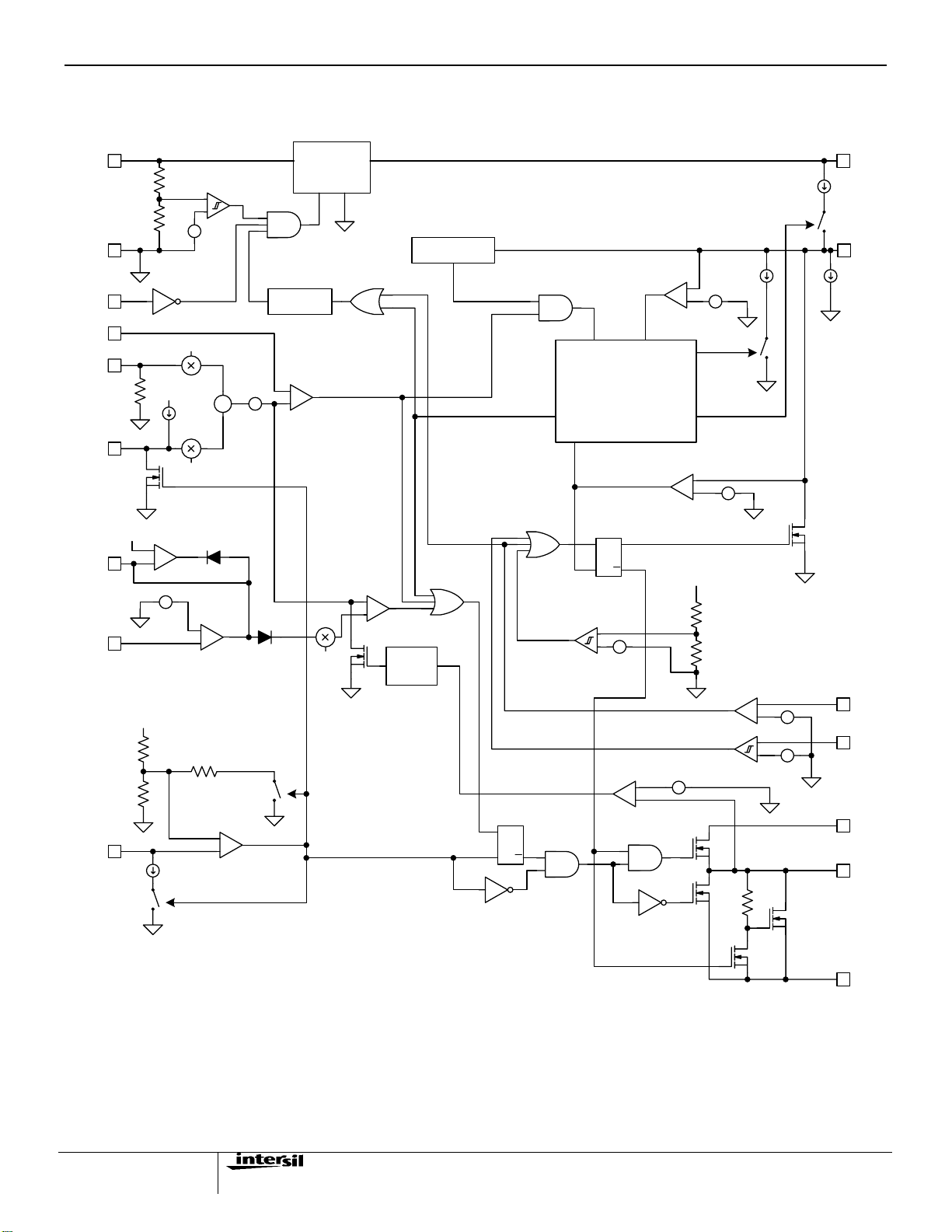
內部電路結构 (ISL6722A)
V
LGND
SLEEP
ISET
ISENSE
SLOPE
COMP
VFB
CC
5K
VREF
SS
+
-
-
2.5V
+
BG
-
0.8
53 µ A
0. 1
SS CLAM P
+
STAR T/STOP
UV C OMPARAT OR
+
-
+
Σ
100 mV
+
ERROR
AMPLIFIE
R
+
-
ISL6722A, ISL6723A
V
REF
5.00 V
ENABLE
SS CH ARGE
VOLTAGE C LAMP
OC
FAULT
OC
OVERCURRENT
SHUTDOWN
DELAY
SS LOW
FAULT
LATC H
SRQ
Q
-
-
+
+
BG
+
-
-
+
SS LOW
COM PARATOR
VREF
STAR T
SS CH ARGED
SET DOMINANT
VREF
UV C OMPARAT OR
4. 65V
RESTA RT
DELAY
OC DETECT
-
+
-
+
OVERCURRENT
COM PARATOR
PWM
COM PARATOR
1/3
+
-
100 nS
BLANKIN G
-
+
4. 375 V
SS DCHG
SS CH GSHT DN
270 mV
SOFT START
CHARGE
CURRENT
25 µ A
ON
-
+
70 µ A
ON
VREF
SS
15 µA
RTCT
20K
30K
VREF
3.0 V/
1. 5V
1mA
ON
12K
OSCILLATOR
COM PARATOR
-
+
+
-
+
-
2.50V
-
-
+
BLANKIN G
ON
COMPARATOR
SRQ
Q
3.0V
-
+
-
+
+
1.45V
36K
OV
UV
V
C
GATE
PGND
2
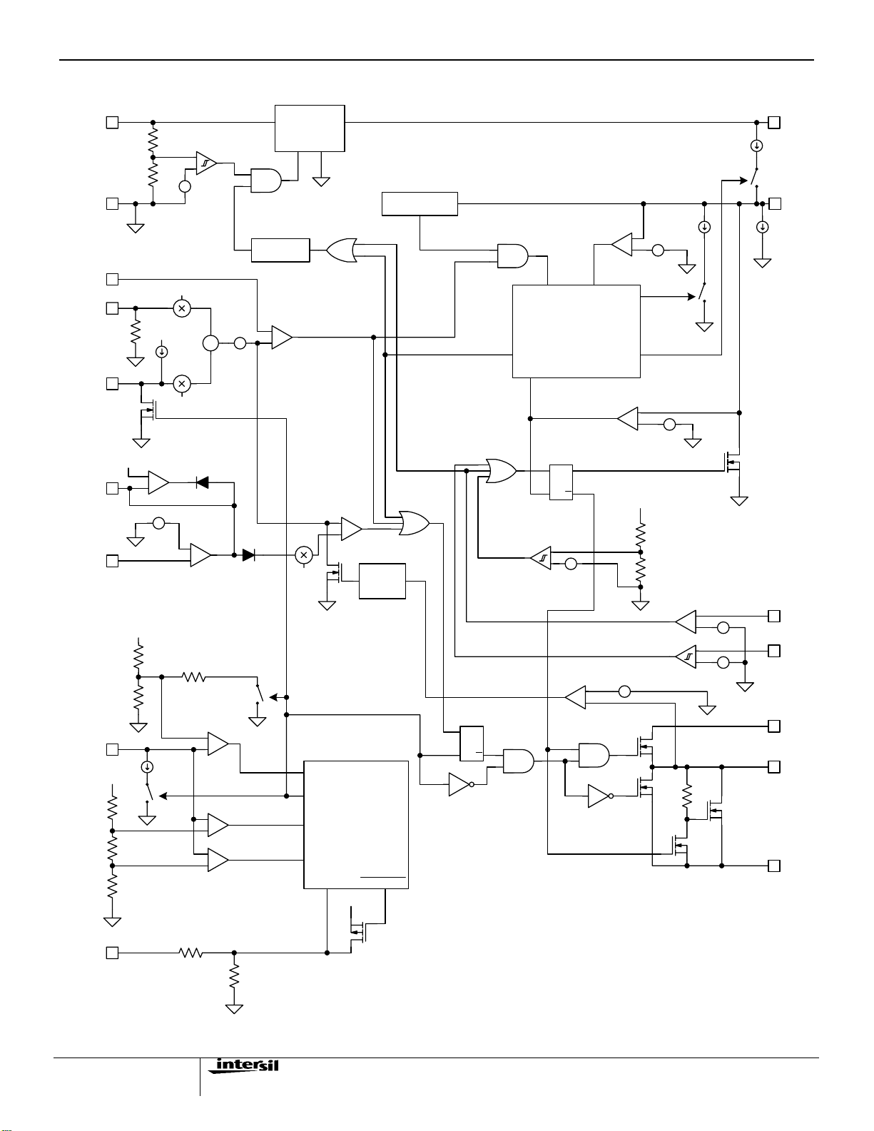
內部電路結构 (ISL6723A)
V
LGND
ISET
ISENSE
SLOPE
COMP
VFB
CC
5K
VREF
SS
+
-
-
2.5 V
BG
0.8
53 µA
0.1
SS CLAM P
+
+
START /STOP
UV COMPARATOR
+
-
-
+
-
Σ
100 mV
+
ERROR
AMPLIFIE
R
+
-
+
ENABLE
RESTAR T
DELAY
-
+
OVERCURRENT
COM PARATO R
V
REF
5. 00 V
1 %
OC DETECT
PWM
COM PARATOR
1/ 3
ISL6722A, ISL6723A
SS CHAR GE
VOLTAGE CLAM P
SS CHARGED
+
-
100 nS
BLANKIN G
START
UV C OMPARAT OR
SET DOMINANT
VREF
4.65V
OC
FAULT
OC
OVERCURRENT
SHUT DOWN
DELAY
SS LOW
FAULT
LATC H
SRQ
Q
-
-
+
+
BG
+
-
SS DCHG
SS CHGSHTD N
-
+
SS LOW
COMPARATOR
VREF
+
4.375 V
270 mV
25 µA
-
-
+
SOFT START
CHARGE
CURRENT
ON
VREF
70 µA
ON
SS
15 µA
RTCT
SYNC
+
-
+
36K
-
2.50V
-
-
+
+
1.45V
VREF
20 K
3.0V
12 K
1.5V
4. 5K
ON
Bi-Directional
Synchronization
OSC IN
CLK OUT
NO EXT SYNC
EXT SYN C BLANKIN G
SYNC IN SYNC OUT
VREF
SRQ
Q
30 K
OSCILLATOR
COMPARATOR
-
+
VREF
4V
2V
1mA
ON
100
+
-
-
+
BLANKIN G
COMPARATOR
-
+
3.0 V
-
+
OV
UV
V
C
GAT E
PGND
3
ISL6722A, ISL6723A
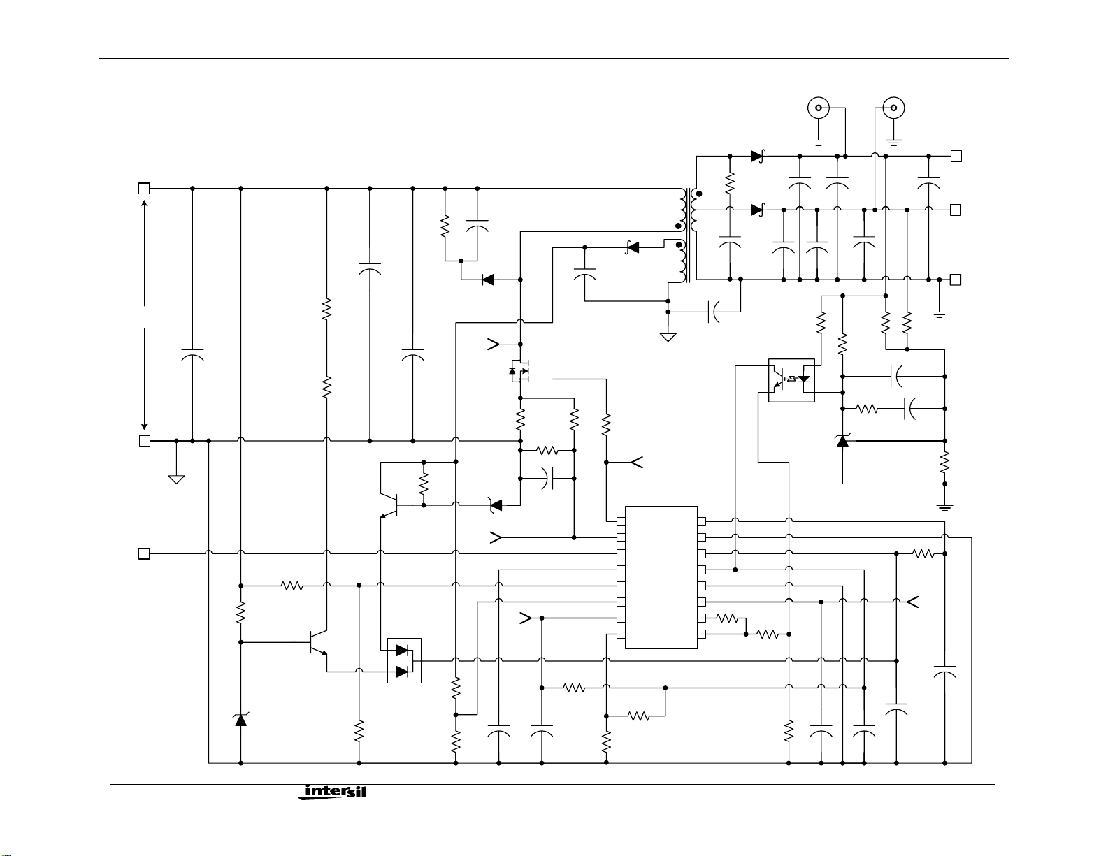
典型應用電路– 48V輸入, 兩個輸出反饋轉換 3.3V @ 2.5A, 1.8V
VIN+
P9
TP1
TP3
CR6
C18
Q1
R4
D1
TP5
R3
R23
C4 U4
VIN-
SLEEP
36 -75 V
R24
C2
R1
C1
R2
Q2
R5
R6
Q3
C3
R25
D2
SP1 SP2
CR5
T1
ISOLATION
XFMR
CR2
C5
R22
TP2
V
ISL6722A
PGND
V
VREF
LGND
SS
COMP
VFB
C
CC
GATE
ISENSE
SLEEP
SLOPE
UV
OV
RTCT
ISET
R21
CR4
C17
C6
R26
R27
C21
C19 C22
+
R16
U2
U3
C15 C16
++
+
C20
R17
R19
C14
R15
R18
C13
R20
R14
TP4
C12
+3 .3V
+1.8V
RETURN
VR 1
R8
C7
R7
R9
4
R10
C8
R11
R12
C9
R13
C11
C10

ISL6722A, ISL6723A
REF
熱性能的資料
Thermal Resistance Junction to Ambient (Typical) θJA (oC/W)
16 Lead SOIC (Note 1)-------------------------------------80
16 Lead TSSOP (Note 1)----------------------------------105
Maximum Junction Temperature -------------------55
Maximum Storage Temperature Range-----------65
Maximum Lead Temperature (Soldering 10s)--------------300
o
C to 150oC
o
C to 150oC
o
C
(SOIC, TSSOP – Lead Tips Only)
額定值
Supply Voltage, VCC, VC -----------GND - 0.3V to +20.0V
GATE ------------GND-0.3V to Gate Output Limit Voltage
PGND to LGND -------------------------------------------+
VREF ---------------------------------------GND – 0.3V to 5.3V
Signal Pins --------------------------------GND – 0.3V to V
Peak GATE Current ------------------------------------------- 1A
ESD Classification
Human Body Model (Per JESD22-A114C.01)--------------------1250V
Charged Device Model (Per JESD22-C101-A)-------------------1000V
0.3V
運行條件
Supply Voltage Range (Typical)------------------9V-18VDC
Temperature Range
ISL6722AAxZ-------------------------------40
ISL6723AAxZ----------------------------- -40
CAUTION: Stress above those listed in “Absolute Maximum Ratings” may cause permanent damage to the device. This is a stress only rating and operation of the
device at these or any other conditions above those indicated in the operational section of this specification is not implied.
Notes:
1) θJA is measured with the component mounted on a low effective thermal conductivity test board in free air. See Tech Brief TB379 for
details.
2) All voltages are with respect to GND.
電气規范
Recommended Operating Conditions, Unless Otherwise Noted. Refer to Block Diagram and Typical Application Schematic.
9V < V
o
C to 105oC
o
C to 105oC
Electrical Specifications
= VC < 20V, RT = 11kΩ, CT = 330pF, TA = -40oC to 105oC (Note 3), Typical values are at TA= 25oC (Continued)
CC
PARAMETER TEST CONDITIONS MIN TYP MAX UNITS
UNDERVOLTAGE LOCKOUT
START Threshold (ISL6722A) SLEEP = 0V 7.95 8.25 8.55 V
START Threshold (ISL6723A) 12.4 13 13.4 V
STOP Threshold 7.4 7.7 8.2 V
Hysteresis (ISL6722A) 0.50 0.55 1.00 V
Hysteresis (ISL6723A) 4.00 5.00 6.00 V
Start-Up Current, ICC V
OC/OV Fault Operating Current, ICC - 200 300
< START Threshold - 100 175
CC
µA
µA
Operating Current, ICC - 4.5 10.0 mA
Operating Supply Current, IC Includes 1nF GATE loading - 8.0 12.0 mA
REFERENCE VOLTAGE
Overall Accuracy
Line, load, TA = 0 - 105°C 4.95 5.00 5.05 V
Line, load, T
= -40 - 105°C 4.90 5.00 5.05 V
A
Long Term Stability TA = 125°C, 1000 hours (Note 5) - 5.00 - mV
Fault Voltage 4.50 4.65 4.75 V
VREF Good Voltage 4.65 4.8 4.95 V
Hysteresis 75 165 250 mV
Operational Current -10 - - mA
Current Limit -20 - - mA
CURRENT SENSE
Input Impedance
5
- 5 -
kΩ

ISL6722A, ISL6723A
電气規范
Recommended Operating Conditions, Unless Otherwise Noted. Refer to Block Diagram and Typical Application Schematic.
9V < V
= VC < 20V, RT = 11kΩ, CT = 330pF, TA = -40oC to 105oC (Note 3), Typical values are at TA= 25oC (Continued)
CC
PARAMETER TEST CONDITIONS MIN TYP MAX UNITS
Offset Voltage 0.08 0.10 0.11 V
Input Voltage Range 0 - 1.5 V
Blanking Time (Note 5) 30 60 100 ns
Gain, ACS
V
ISET
= ∆ISET/∆ISENSE
A
CS
0.77 0.79 0.81 V/V
V
= 0V, VFB = 2.3V,
SLOPE
= 0.35V, 1.5V
ERROR AMPLIFIER
Open Loop Voltage Gain (Note 5) 60 90 - dB
Gain-Bandwidth Product (Note 5) - 15 - MHz
Reference Voltage Initial Accuracy VFB = COMP, TA = 25°C (Note 5) 2.465 2.515 2.565 V
Reference Voltage V
= COMP 2.44 2.515 2.590 V
FB
COMP to PWM Gain, ACOMP COMP = 4V, TA = 25°C 0.31 0.33 0.35 V/V
COMP to PWM Offset COMP = 4V 0.51 0.75 0.88 V
FB Input Bias Current V
= 0V -2 0.1 2
FB
COMP Sink Current COMP = 1.5V, VFB = 2.7V 2 6 - mA
COMP Source Current COMP = 1.5V, VFB = 2.3V -0.25 -0.5 - mA
COMP VOH VFB = 2.3V 4.25 4.4 5.0 V
COMP VOL VFB = 2.7V 0.4 0.8 1.2 V
PSRR Frequency = 120Hz (Note 5) 60 80 -
SS Clamp, VCOMP SS = 2.5V, VFB = 0V, I
= 2V 2.4 2.5 2.6 V
SET
Electrical Specifications
µA
dB
OSCILLATOR
Frequency Accuracy 289 318 347 kHz
Frequency Variation with VCC TA = 105°C (F
T
= -40°C (F
A
- F9V)/F9V - 2 3
20V
- F9V)/F9V 2 3
20V
%
Temperature Stability (Note 5) - 8 - %
Maximum Duty Cycle (Note 6) 68 75 81 %
Comparator High Threshold - 3.00 - V
Comparator High Threshold w/Ext. SYNC
(ISL6723A)
(Note 5) - 4.00 - V
Comparator Low Threshold - 1.50 - V
Discharge Current
TA = 0 - 105°C 0.75 1 1.2
T
= -40 - 105°C 0.70 1 1.2
A
mA
SOFTSTART
Charging Current SS = 2V -40 -55 -70
µA
Charged Threshold Voltage 4.26 4.5 4.74 V
Initial Overcurrent Discharge Current
Sustained OC Threshold
< SS < Charged Threshold
30 40 55
µA
6
電气規范
ISL6722A, ISL6723A
Electrical Specifications
Recommended Operating Conditions, Unless Otherwise Noted. Refer to Block Diagram and Typical Application Schematic.
9V < V
= VC < 20V, RT = 11kΩ, CT = 330pF, TA = -40oC to 105oC (Note 3), Typical values are at TA= 25oC (Continued)
CC
Overcurrent Shutdown Threshold Voltage
Charged Threshold minus,
= 25°C
T
A
0.110 0.125 0.140 V
Fault Discharge Current SS = 2V 0.25 1.0 - mA
Reset Threshold Voltage TA = 25°C 0.22 0.27 0.31 V
SLOPE COMPENSATION
Charge Current
Slope Compensation Gain
Discharge Voltage V
SLOPE = 2V, TA= 0 - 105°C -45 -53 -65
T
= -40 - 105°C -41 -53 -65
A
Fraction of slope voltage added to
ISENSE, T
RTCT
= 25°C
A
= 4.5V - 0.1 0.2 V
0.1 0.103 0.107 V/V
µA
µA
GATE OUTPUT
Gate Output Limit Voltage
Gate VOH
Gate VOL
Peak Output Current
= 20V, C
V
C
= 0mA
I
OUT
- GATE, VC = 10V,
V
C
= 150mA
I
OUT
GATE - PGND, I
I
= 20V, C
V
C
(Note 5)
= 1nF,
GATE
11.0 13.5 16.0 V
- 1.5 2.2 V
= 150mA 1.2 1.5
OUT
= 10mA 0.6 0.8
OUT
= 1nF
GATE
- 1 - A
V
Output “Faulted” Leakage VC = 20V, UV = 0V, GATE = 2V 1.2 2.6 - mA
Rise Time
Fall Time
Minimum ON time
= 20V, C
V
C
1V < GATE < 9V
= 20V, C
V
C
1V < GATE < 9V
= 0.5V; VFB = 0V; VC = 11V
I
SET
ISENSE to GATE w/10:1 Divider R
= 4.75V through 1kΩ
GATE
GATE
= 1nF
= 1nF
TCT
- 60 100 ns
- 15 40 ns
- - 110 ns
(Note 5)
OVERCURRENT PROTECTION
Minimum ISET Voltage - - 0.35 V
Maximum ISET Voltage 1.2 - - V
ISET Bias Current V
= 1.00V -1 - 1
ISET
µA
Restart Delay TA = 25°C 150 295 445 ms
OV & UV VOLTAGE MONITOR
Overvoltage Threshold 2.4 2.5 2.6 V
Undervoltage Fault Threshold 1.38 1.45 1.52 V
Undervoltage Clear Threshold 1.41 1.53 1.62 V
Undervoltage Hysteresis Voltage 20 50 100 mV
UV Bias Current VUV = 2.00V -1 - 1
OV Bias Current VOV = 2.00V -1 - 1
µA
µA
7

ISL6722A, ISL6723A
Electrical Specifications
電气規范
SLEEP (ISL6722A)
SLEEP Input Threshold Voltage Active High 1 1.5 2.7 V
SLEEP Input Current V
ICC @ SLEEP VCC = 15V - 175 210
SYNCHRONIZATION (ISL6723A)
Input High Threshold - - 2.5 V
Input Pulse Width 25 - - ns
Input Frequency Range (Note 5)
Input Impedance - 4.5 -
VOH
VOL R
SYNC Advance
Output Pulse Width C
NOTES:
3. Specifications at -40
4. This is the V
5. Guaranteed by design, not 100% tested in production.
6. This is the maximum duty cycle achievable using the specified values of R
using other values for R
current consumed when the device is active but not switching. Does not include gate drive current.
CC
Recommended Operating Conditions, Unless Otherwise Noted. Refer to Block Diagram and Typical Application Schematic.
9V < V
= VC < 20V, RT = 11kΩ, CT = 330pF, TA = -40oC to 105oC (Note 3), Typical values are at TA= 25oC.
CC
= 4.0V 11 25 46
SLEEP
= 4.5kΩ
R
LOAD
= open - - 0.1 V
LOAD
SYNC rising edge to GATE falling
edge, C
GATE
= 100pF 50 - - ns
SYNC
o
C and 105 oC are guaranteed by 25
and CT. See Equations 1-4.
T
= C
= 100pF
SYNC
o
C test with margin limits.
and CT. Larger or smaller maximum duty cycles may be obtained
T
0.65x Free
Running
2.5 - - V
- 25 55 ns
- 1 MHz
µA
µA
kΩ
8

典型性能曲線圖
ISL6722A, ISL6723A
1.002
1
0.998
0.995
0.993
Normalized EA Reference
0.991
40 10 20 50 80 110
Temperature (C)
FIGURE 1 EA REFERENCE VOLTAGE vs TEMPERATURE FIGURE 2 V
1.002
1
0.998
0.995
Normalized Vref
0.993
0.991
40 10 20 50 80 110
Temperature (C)
REFERENCE VOLTAGE vs TEMPERATURE
REF
3
1.002
0.996
0.989
0.983
0.976
Normalized Frequency
0.97
40 10 20 50 80 110
Temperature (C)
FIGURE 3 OSCILLATOR FREQUENCY vs TEMPERATURE FIGURE 4 CAPACITANCE vs FREQUENCY
1-10
100
CT=
100pF
220pF
330pF
470pF
680pF
10
20 30 40 50 60 70 80 90 10010
RT (kΩ)
1000pF
2000pF
9

ISL6722A, ISL6723A
各管腳簡介
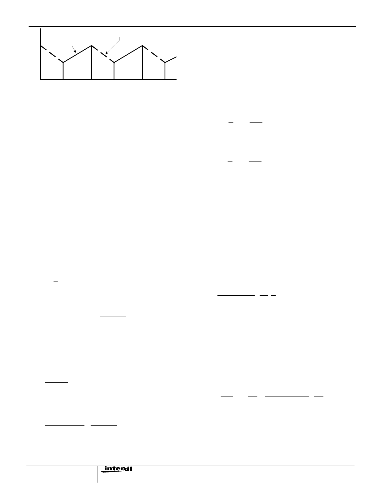
SLOPE
每一個開關周期, 內置的電流源會充電一個外部電容。由此產
生的斜升轉換后与ISENSE信號疊加。可以用這個方法來提高
ISENSE斜升率, 為提高無噪音的免疫力或是提高對于占空比
大于50%的控制環路的穩定性。
SLEEP (ISL6722A)
這是一個邏輯輸入控制信號可以用來禁止控制器以及啟動低
功耗待机模式。SLEEP是高態有效信號。
SYNC (ISL6723A)
雙向同步信號是用來協調多系統的工作頻率。通過連接每個
單元的SYNC引腳在一起或者利用外界主控時鐘可以取得同
步。即使使用外界主控時鐘, 振蕩器的定時電容, C
使用的。第一個取得這個信號的單元將起主導控制作用。
RTCT
這是振蕩器的時序控制引腳。工作頻率和最大占空比可用在
在這個引腳和V
LGND之間挎接一個電容, C
之間挎接一個電阻, RT, 以及在這個引腳和
REF
來決定。這個振蕩器能產生
T
100KHz至1.0MHz的鋸齒波型。充電時間, TC, 放電時間, TD,
開關頻率, FSW, 以及最大占空比, D
, 可以用以下的等式來
MAX
求:
CRT ••≈ 655.0 S EQ. 1
TTc
6.3001.0
−•
R
T
(
••−≈
LNCRT S EQ. 2
TTD
R
)
9.1001.0
−•
T
, 也是必須
T
這個引腳是過壓監視輸入端。這個信號与內置的2.5V基准電
壓作比較來檢測過壓狀況。
UV
這是欠壓監察輸入引腳。UV信號与內置 1.45V臨限值比較決
定其欠壓條件。
ISENSE
這是電流感應比較器的輸入端。這個控制器有兩個電流感應
比較器, 一個PWM比較器用作峰值電流控制模式, 一個過流保
護比較器。過流保護比較器的臨界值可以通過ISET引腳來設
置。
超過過流臨界將引發延遲的切斷過程。一旦過流狀況被檢測,
軟啟動的充電源會被抑制, 而軟啟動電容開始放電。放電至小
于4.375V時(持續過流臨界), 切斷產生并且門极輸出將會被拉
低。當軟啟動電壓達到0.27V時 (重設臨界), 軟啟動將開始。
如果在50µS時間內軟啟動電容沒有跌落低于4.375V(持續過
流臨界), 過流情況消除,切斷不會發生, 軟啟動電壓复位。
LGND
器件上所有模擬功能都以這個小信號基准為地。
PGND
這個引腳為門极驅動器提供專門的接地。LGND 引腳与
PGND 引腳必須用与引腳很近并且很短的 PCB 線跡在控制器
的外面相連。這對于防止巨大的開關電流流經控制器內部的
接地面是相當有必要的 (從 V
到 PGND 跨接一個低 ESR 的
C
0.1µF 或更高的電容來去耦) 。
SW
max
=
Hz EQ. 3
TTF+
CD
FTD •=
EQ. 4
SWC
1
圖4可以用來選擇一個已知瀕率的電容和電阻值。
COMP
COMP引腳是誤差放大器的輸出端以及PWM比較器的輸入
端。控制環路頻率補償网絡跨接在COMP引腳与FB引腳之
間。
ISL6722A和ISL6723A具備內置全周期軟啟動功能。軟啟動是
通過最大COMP電壓鉗位來實現的。
FB
反饋電壓輸入端与誤差放大器的反相輸入端連接。誤差放大
器的同相輸入端与內置基准電壓連接。
OV
10
GATE
這是芯片的輸出端, 是一個高電流功率驅動器可以用來以峰值
為1A的電流驅動一個功率MOSFET。這個驅動器的輸出端將
被拉低當V
低于其欠壓臨界值。
CC
輸出端的鉗位電壓是~13.5V。高于這個電壓值不可以与
GATE引腳直接連接。為了防止過沖或下沖電壓, 每個輸出端
提供非常低的阻抗。
V
C
這個引腳是為門极驅動輸出提供分開的集電极電源。把V
和
C
PGND分開能幫助芯片的模擬電路与高功率的門极驅功噪聲
去耦。(從V
到PGND跨接一個低ESR的0.1µF或更高的電容
C
來去耦) 。
V
CC

ISL6722A, ISL6723A
VCC是控制器的電源輸入端。雖然靜態電流, ICC, 很小, 但是它
与頻率有直接的關系。要优化抗扰度, 用一個陶瓷電容器盡可
能靠近并挎接在V
總電源電流, (I
和LGND引腳。
CC
加上ICC), 取決于門极負載狀況, 將會更高。總
C
電流是靜態電流和平均門极輸出電流之和。平均門极輸出電
流的大小取決于已知工作頻率F
, 以及MOSFET門极輸出負
SW
載電容電荷, Qg,可以用以下的公式來計算:
FQI •= A EQ. 5
SWggate
VREF
這是5.00V的基准電壓輸出端。可連接0.01
µF或更高的電容至
LGND以作濾波這輸出所需。使用電容小于這個值可能會引起
振蕩。
SS
在這個引腳与LGND之間連接一個軟啟動時序電容能夠控制軟
啟動的時間。這個電容值能夠決定在軟啟動時占空比上升的
速度, 控制過流切斷的延遲。
ISET
在這個引腳上0.35V至1.2VDC電壓可以用來設置脈沖-脈沖過
流臨界。當過流發生時, SS軟啟功電容將開始放電并開始過
流延遲關閉的過程。
功能概述
主要特點
ISL6722A和ISL6723A電流模式PMW最适用于采用了加強控
制和監督能力的低成本反激和正激型拓扑結构的變換器。
ISL6722A和ISL6723A具有可調過壓和欠壓門限, 過流保護,
間歇延遲的性能, 需要极少外部元件。其它性能包括: 峰值電
流模式控制,可調軟啟動, 斜率補償, 可調振蕩器頻率和低功
率靜態模式。
振蕩器
ISL6722A和ISL6723A通過改變RTCT引腳的電阻和電容可調
鋸齒振蕩器頻率高達1MH。(指定頻率的電阻和電容請參考圖
4) 。
實現同步操作 (ISL6723A)
鐘信號, 主要元件 SYNC 采用 SYNC 信號控制。如果信號產
生于前 1/3 的開關周期, 可忽略外部 SYNC 脈沖。
在正常運行情況下, RTCT 電壓充電由 1.5 至 3.0V, 周期循
環。當到達 3.0V 門限值時就會產生時鐘和 SYNC 信號。若
在后 2/3 的充電周期內檢測出外部時鐘信號, 振蕩器會轉換成
外部同步模式, 且根据外部 SYNC 信號來終止振蕩器周期。
此模式是不會產生 SYNC 信號。如果 RTCT 電壓超過 4.0V
(換而言之: 沒有外部的 SYNC 信號終止周期), 振蕩器會回复
到內部時鐘模式且會產生 SYNC 信號。
實現軟啟動運作
ISL6722A 和 ISL6723A 使用外部電容和內部電流電源來作軟
啟動。軟啟動降低啟動期間的電壓和浪涌電流。
啟動時,軟啟動電路把誤差放大器輸出 (COMP 引腳) 鉗位于
一個与軟啟動電壓相應的值。 誤差放大器輸出隨著軟啟動電
容電壓增加而增加, 這使軟啟動期間的輸出脈寬可從零增加到
穩定狀態運行時的占空比。當軟啟動電壓超過誤差放大器電
壓,軟啟動完成。軟啟動強制受控輸出電壓上升。軟啟動開
始于起動或因故障而复位時。軟啟動電壓鉗位于 4.5V。
門极驅動器
ISL6722A和ISL6723A的輸出可灌出和吸入1A峰值電流。獨
立集成供應 (V
) 和功率地 (PGND) 引腳可把大功率門极驅動
C
器噪音隔离開IC的模擬電路。要限制峰值電流通過IC,可在
IC (門极引腳) 的推拉輸出和MOSFET的門极之間放置一個外
部電阻。而這個小串聯電阻能減少由線組寄生電感和驅動器
的輸入電容的共振所產生的振蕩。
斜率補償
對于最大占空比少于50%的應用可采用斜率補償來改善噪音
干扰,尤其是在較低負載時。防止噪音干扰所需的斜率補償
額可以憑經驗确定, 但一般約為10%的總電流反饋信號。對于
最大占空比高于50%的應用則需用斜率補償防止不穩定。斜
率補償是通過加接額外斜坡以調整電流反饋信號的一种方
法。
最小斜坡補償應相當于1/2的電感下坡。可是, 加接過多的斜
率補償會導致控制環表現為電壓模式控制多于電流模式控
制。
ISL6723A 可在 SYNC 引腳設置一外部時鐘或通過把多重 IC
的 SYNC 引腳連接在一起來實現同步化。如果用外部主時鐘
信號, 振蕩器必須至少有 65%的 IC 固有頻率才可實現同步
化。外部主時鐘信號應有一大于 20ns 的脈寬。如果不用主時
11
ISL6722A, ISL6723A
Downslope
Cu rrent Sense Sign al
ISENSE Signal (V)
Time
Figure 5
加在SLOPE引腳的最小電容值為
Cslope •×=
1024.4 F EQ. 6
Vslope
ton
−6
式中:ton是導通時間, Vslope是加在電流反饋信號作為斜坡
補償的電壓值。大致上斜坡值是所需最小值的2-3倍。
例如:
假設在關斷期間, ISENSE引腳的電感電流信號降低125mV,
且開關頻率, Switching Frequency, Fsw = 250kHz
占空比, Duty Cycle, D = 60%
ton = D/Fsw = 0.6/250E3 = 2.4μs
toff = (1 - D)/Fsw = 1.6μs
确定下坡:
下坡= 0.125V/1.6μs = 78mV/μs。現确定導通時間末端電流
感應信號所需增加的電壓值。
1
2
mVVslope 944.2078.0
=••= EQ. 7
因此,
−
1024.4(min)
•×=
094.0
pFCslope 110
≈
EQ. 8
6
−
104.2
×
6
所計算出的值, 110pF, 為所需的最小斜坡補償。此例中适當
的斜坡補償電容應為所得值的1/2-1/3, 即68-33pF之間。
較精确的斜坡補償可從小信號電流模式的模型[1]求得。它顯
示了自然抽樣調制器的增益。Fm,無斜率補償,是
1
=
EQ. 9
TswSnFm•
式中:Sn是鋸齒信號的斜率。Tsw是開關頻率。若加接一外
部斜坡,調制器的增益則為
Fm
=
1
)(
•+
1
=
SnTswmTswSeSn
c
EQ. 10
式中:Se是外部斜坡的斜率以及
Se
m
c
EQ. 11
+= 1
Sn
50%的振蕩器頻率的雙极阻尼系數決定外部斜坡的基准額。
若Q系數設置為1,雙极會臨界阻尼;Q>1時,欠阻尼; Q<1
則會過阻尼。欠阻尼會引起電流環不穩定。
Q
π
1
c
EQ. 12
)5.0)1((
−−=Dm
式中:D是最大占空比。設定Q = 1,求得Se為
1
(( −
SnSe
π
1
)5.0
1
−+=D
EQ. 13
)1
因為Sn和Se分別是電流斜坡和外部斜坡導通時的斜率,与導
通時間 (TON) 之積是導通時間 (TON) 內所產生的電壓變化。
VnVe
式中:V
1
(( −
π
是導通時間內電流反饋信號的變化,Ve是加外部斜
n
1
EQ. 14
−+=D
)1
)5.0
1
坡所增加的電壓。
對于降壓拓扑結构, 用輸出電壓,電流傳感器元件和輸出電感
可求出V
Ve
式中:R
, 代入等式15, 可求出Ve。
n
••
= D
CS
RcsVoTsw
•
LN
OCT
是電流感應電阻,NCT是電流變壓器變比,LO是輸
Ns
Np
1
( −+•
π
)5.0
EQ. 15
出電感,VO是輸出電壓,而NS和NP分別是副邊和原邊線圈。
對于反激型拓扑結构, 用輸出電壓,電流傳感器元件和原邊電
感可求出V
= D
Ve
式中:RCS是電流感應電阻,NCT是電流變壓器變比,L
原邊電感,V
, 代入等式16, 可求Ve
n
••
RcsVoTsw
•
LN
PCT
是輸出電壓,而NS和NP分別是副邊和原邊線
O
Np
Ns
1
( −+•
π
)5.0
V EQ. 16
是
P
圈。如果不采用電流變壓器, 則NCT = 1。
為討論之用, 會更深入地論述反激型拓扑結构。而降壓拓扑結
构的論述可見ISL6753的數据資料。
原邊電流通過電流感應變壓器的反射而在電流感應電阻上產
生的電流感應信號為,
R
CS
CS
N
CT
CS
V •
式中:V
N
S
I
O
+•=
)((
N
P
是橫跨電流感應電阻的電壓,IO是輸出電流的門限
TVD
••−
)1(
L
2
P
N
SWO
P
)
V EQ. 17
N
S
值。
由于峰值電流門限值是取決于ISET,若輸出負載為此電流門
限值, 總電流反饋信號和外部斜坡電壓必須加到這個伏數。
12

ISL6722A, ISL6723A
ISETVV
CSe
=+•+ 100.0)8.0( EQ. 18
式中包括內部增益和IC的失調電壓。把等式15和17代入等式
18可求得其RCS值
NISET
•−
)1.0(
R
=
CS
NVT
••
NL
•
SP
1
POSW
(
π
CT
N
S
ID
•+−+•
8.0)1.06.0
O
N
P
EQ. 19
即ISL6722A和ISL6723A用SLOPE輸入實現的斜率補償。用
等式16确定Ve值, 再乘以10就是SLOPE輸入所需的電壓。
•
TI
C
SLOPE
式中I
=
是SLOPE的內部充電電流, 典型值為53μA。
SLOPE
onSLOPE
EQ. 20
10•
V
e
過壓和欠壓監控
OV和UV信號是窗口比較器的輸入, 用來監控變換器輸入電壓
平。若電壓跌落至超出指定的操作范圍就會引起關斷故障。
過壓 (OV) 故障, 在約295ms复位時間內ICC供應電流降低至
200μA。若故障清除, 一個軟啟動周期將重新運作。否則會產
生另一個關斷周期。欠壓 (UV) 狀況也會導致關斷故障, 但元
件不會進入低功率模式和故障清除時不會發生重啟延遲。
Vin和LGND間的電阻分割器的每個輸入決定工作閥。欠壓
(UV)門限有一個75mV的固定遲滯。
過流運作
過流門限根据ISET引腳的供應電壓來設定。從VREF到LGND
用一電阻分壓器來設定過流門限。ISET門限應設在相應于所
要峰值輸出電感電流加上斜率補償迭加效應的水平。
軟啟動周期完成后,過流延遲關斷保護才啟動。如果檢測出
過流情況,軟啟動充電電流電源就會中止,啟動放電電流電
源。軟啟動電容通過40
50µS時間內,如果軟啟動電容由4.5V放電至4.375V,輸出停
止且軟啟動電容放電。輸出持續停止而ICC電流在約295ms內
會跌落至200
µA。然后開始新的軟啟動周期。過流 (OC) 保護
的關斷和重啟通常視為因重复啟動和關斷的間歇運作。
如果在軟啟動電壓降至的4.375V前,且過流情況停止至少
50µs,軟啟動充電和放電電流會恢复正常運作,軟啟動電壓
會复位。
通過設定ISET的電壓為超過誤差放大器電流控制電壓或約
1.5V就不會產生間歇過流 (OC) 保護。
圖6顯示了軟啟動期間的過流狀態。ISENSE’表示輸入到過流
比較器的ISENSE值。
µA電源放電。過流情況停止后,在
4.5 V
SS
ISET
ISENSE '
GATE
FIGURE 6 PULSE-BY-PULSE OC BEHAVIOR DURING SS
盡管存在過流情況, 在軟啟動(SS)周期完成前不會發生關斷。
在軟啟動周期內只有峰值電流限制運作。如果軟啟動周期完
成后仍存在過流情況, 就會啟動延遲過流關斷, 如下圖 7 所
示。
SS
ISET
ISENSE '
GATE
FIGURE 7 OC SHUTDOWN BEHAVIOR
4 .375 V
GND
4.5 V
295 ms
如果關斷前過流情況停止, 軟啟動電壓則會复位。如圖8所
示。當負載下降低于過流門限值且在50
µS時間內軟啟動電容
沒有跌落低于4.375V,過流情況會消除,軟啟動電壓复位。
SS
4.375 V
ISET
ISENSE '
GATE
FIGURE 8 OC RECOVERY PRIOR TO SHUTDOWN
OC
4.5 V
50 µS
上升沿封鎖
用上升沿封鎖電路可消除ISENSE最初100ns的電流反饋信號
輸入。當門极 (GATE) 輸出上升沿超過3.0V時開始封鎖周
期。上升沿封鎖可防止因寄生元素而產生尖峰電流所引起
PWM比較器和過流比較器的錯誤触發。
故障状况
如果VREF跌落低于4.65V, OV輸入超過2.50V, 或UV輸入跌
落低于1.45V就會發生故障狀況。檢測出故障時, GATE輸出
就會截止且軟啟動電容會迅速地放電。當故障清除后以及軟
啟動電壓低于复位臨限時, 一個軟啟動周期將重新運作。
接地要求
13

ISL6722A, ISL6723A
為使這個器件能理想地工作,應該要仔細布局。特別是應用
一個好的接地面,部分的接地面必須設只為高di/dt電流輸
出。功率地 (PGND) 与邏輯接地 (LGND) 分開連接在一單
點。 V
應以一個好的高頻電容直接旁接到地PGND。輸入功
C
率的回路連接和主輸入電容應連接于PGND。
參考設計
ISL6722A 典型應用于傳統雙端輸出的10W間斷模式反激
DC/DC變換器。ISL6722AEVAL1示范單元引用了此設計且可
供測定。輸入電壓是36V-75V直電流, 兩個輸出是3.3V @
2.5A和1.8V @ 1.0A。可用兩個輸出的加權和實現橫向調節。
電路元件簡介
此變換器的設計可分成下列功能塊:
輸入存儲和濾波電容: C1, C2, C3
隔离變壓器: T1
原邊電壓鉗位: CR6, R24, C18
啟動偏壓調節器: R1, R2, R6, Q3, VR1
運行偏壓与調節器: R25, Q2, D1, C5, CR2, D2
主功率 MOSFET: Q1
電流感應网絡: R4, R3, R23, C4
反饋网絡: R13, R15, R16, R17, R18, R19, R20, R26, R27,
C13, C14, U2, U3
控制電路: C7, C8, C9, C10, C11, C12, R5, R6, R8, R9, R10,
R11, R12, R14, R22
輸出整流和過濾: CR4, CR5, C15, C16, C19, C20, C21, C22
副邊的緩沖器: R21, C17
設計標准
選擇以下設計要求:
開關頻率, Fsw: 200kHz
Vin: 36 - 75V
Vout (1): 3.3V @ 2.5A
Vout (2): 1.8V @ 1.0A
Vout (偏壓): 12V @ 50mA
Pout: 10W
效率, Efficiency: 70%
最大占空比, Maximum Duty Cycle, Dmax: 0.45
變壓器設計
反激型變壓器的設計是繁瑣的且多次重复的過程, 要有丰富的
經驗才可達到滿意的效果。這個設計過程有許多折衷之處, 對
相同的要求/指標, 即使經驗丰富的設計師也會有不同的設計
方案。為了清晰起見, 迭代反复設計過程將不在此討。
簡略的設計過程如下:
• 選擇适于此應用的磁心的几何形狀。高度, 占位面積, 安裝要
求, 以及工作環境將會影響到此選擇。
• 選擇适當磁心的材料 (可能多于一种) 。
• 選擇适合操作的最大磁通量密度。
• 選擇磁心的尺寸大小。磁心体積將取決于磁心結构儲存能量
的能力, 必須繞的圈數, 和所要的線規。在通常的情況下, 窗口
面積 (繞組的空間) 以及功率損耗將會決定最終的選擇。對于
反激型的變壓器, 其儲存能量是決定磁心体積的臨界系數。磁
路的磁心橫截面積和气隙的長度決定能量的儲存能力。
• 确定适合操作的最大磁通量密度。所允許的磁通密度由工作
頻率, 磁心材料的選擇以及工作環境來決定。初次選擇所适當
的磁通密度往往是比較困難的。通常一個合意的設計往往是
利用了最大的磁通密度, 但是有時也會因為繞線的几何形狀而
選用較大的磁心。
• 确定原邊線圈的圈數。
• 决定匝比。
• 選擇每個繞組的線規。
• 确定繞線次序和絕緣材料要求。
• 核實設計。
輸入功率: Pin=Pout/Efficiency = 14.3W (use 15W)
最大導通時間: Ton(max) = Dmax/Fsw = 2.25μs
平均輸入電流: Ivan(in) = Pin/Vin(min) = 0.42A
峰值原邊電流:
inIavg
Ippk
•
= EQ. 21
)(2
TF
•
ONSW
(max)
A
87.1
=
最大原邊電感:
TV
•
ONin
L
= EQ. 22
P
(max)
I
(max)(min)
PPK
選擇适合的原邊電感為 40
=
µH。
H
µ
3.43
磁心結构必須可在每個開關周期輸送能量到副邊以保持特定
的輸出功率。
+
SW
VdVout
Joules
•
VoutF
EQ. 23
•=∆
Poutw
式中 Δw 是每個周期轉換時所需的能量, Vd 橫跨輸出整流器
的電壓降。
帶气隙的鐵氧体磁心結构的能量儲存能力取決于气隙, 可表示
為:
2
=•=
IAeffV
gg
∆••
w
µ
o
2
∆
B
3
m EQ. 24
14

ISL6722A, ISL6723A
式中 Aeff 是有效的磁心橫截面積, 單位為 m2; lg 是气隙的長
度, 單位為米。μo是真空磁導率(4π • 10-7), ΔB 是通量密度的
變化, 單位為特斯拉。
較小气隙的磁心結构無法提供足夠的輸出功率。相反, 若气隙
的長度過大, 間隙周圍會產生磁場邊緣, 且增加气隙体積。通
常允許有部分邊緣, 但過多的邊緣會增加間隙周圍的繞組損耗
從而導致元件過熱。一旦找到适合的磁心与間隙組合, 便開始
了迭代反复的設計過程。展開和檢驗設計以易組裝和減少內
熱。如果磁心沒有足夠的繞線空間, 則需要一個有較大窗口面
積的磁心。若變壓器工作時發熱, 可用較低通量密度(較多的
原邊線圈, 較低的工作頻率), 選用損耗少的磁心材料, 改變繞
組的几何圖形(繞線次序), 用粗號線或多重繞線, 或改變所用線
狀(例如: 絞合線) 。
為了簡單化, 只對最后部分的設計作更進一步的描述。選擇
值為 25 nH/N2 的 N87 間隙材料的 EPCOS EFD 20/10/7
A
L
磁心, 可有較多的气隙存儲能量, 但需有足夠的窗口面積。
6
1031−•=Aeff
−
1056.1lg
•= m
2
m
3
通量密度 ΔB 仅是 0.069T 或 690 高斯 (一個相對較低的
值) 。
因此
2
AeffN
µ
L
=
P
原邊線圈的圈數 N
••
Po
lg
H
µ
EQ. 25
可用 EQ.25 計算, 其結果為 Np = 40圈。
p
副邊線圈的圈數也可計算如下:
)(lg
TVdVout
•+•
r
N
≤
S
µ
oP
EQ. 26
AeffIppkN
•••
式中 Tr 是磁心复位所需的時間。由于是間斷 MMF 模式操作,
在關斷期間磁心必須完全复位。要保持間斷模式操作, 允許磁
心复位的最長時間是 Tsw - Ton(max), 式中 Tsw = 1/Fsw。最
小時間取決于應用和設計師根据所知的副邊繞線 RMS 和波紋
電流對于輸出電容應力隨复位時間減少而增加而作判斷。運
用公式 T = Tsw - Ton (max) = 2.75μs, 求得 3.3V 輸出的最大
副邊線圈的圈數 (Ns) 是 5.52 圈。
接著, 确定線規。原邊繞組的 RMS 電流可用下式計算:
(max)
IppkI
rmsP
)(
Ton
••=3
A EQ. 27
Tsw
其他繞組的峰值和 RMS 電流值可用下式計算:
Ispk••=
2
TswIout
Tr
IoutIrms
A EQ. 28
Tsw
••=32
A EQ. 29
Tr
•
原邊繞組的 RMS 電流是 0.72A, 3.3V 輸出的是 4.23A, 1.8V
輸出的是 1.69A, 以及偏壓繞組的是 85mA。
要減少變壓器漏感, 原邊繞組分成兩個截面并行連接, 這樣其
他的繞組可夾放在中間。配置輸出繞組使 3.3V 繞線的分接頭
為 1.8V 繞線。分接 1.8V 輸出需要副邊繞組一起傳導兩個輸
出的合成電流。副邊線規必須据此選擇。
電線的電流傳輸容量的選擇是綜合考慮了其性能, 体積, 和成
本。它受許多設計約束如工作頻率(波形的諧波含量) 和繞組
鄰近 /几何圖形。通常每安培為 250 至 1000 圓密爾。圓密爾
(Circular Mils) 是直徑為 0.001 英寸 (1 密爾) 的圓形面積。隨
著工作頻率的增加, 電線的交流 (AC) 電阻也會因表層和鄰近
效應而增加。用粗號線可減少此效應, 或用多股線并聯。有些
實例中必需用絞合線。
繞線配置選擇是:
原邊繞線 #1: 40T, 2 #30(雙線)
副邊繞線: 5T, 0.003 英寸(3 密爾)銅箔接在 3T
偏壓繞線: 17T #32
原邊繞線#2: 40T, 2 #30(雙線)
內部空間和絕緣系統設計以原邊和副邊繞組之間的額定為
1500V 直流 (DC) 絕緣負荷。
功率 MOSFET 選擇
主開關 MOSFET 的選擇必需考慮應用中的電壓和電流應力,
元件的功率損耗, 体積, 以及其成本。
副邊線圈圈數的确定同樣取決于輸出次數和其所要的匝比。
如果采用肖特基輸出整流器, 假設其正向電壓降為 0.45V, 兩
個輸出電壓 3.3V 和 1.8V 所需的線圈比例是 5:3。
副邊繞組的匝比是 5:3, 設 Ns1 = 5 圈和 Ns2 = 3 圈, 用這些副
邊線圈數求得复位時間, Tr = 2.33μs 或約 47%的開關時間, 是
一個合意的結果。
偏壓繞組線圈同樣可計算, 只需用二极管的0.7V正向電壓降,
便可求出12V偏壓的線圈數的整數為17圈。
15
變換器的輸入電壓是 36-75V 直流 (DC)。由于隔离變壓器的
原邊繞組可能會出現反饋電壓, 建議用額定電壓為 150V 的
MOSFET。
MOSFET 工作損耗可分成三种類型: 傳導, 開關和門极驅動損
耗。
傳導損耗來自 MOSFET 導通時的阻抗。
2
IprmsrPcond
•= W EQ. 30
ONDS
)(
ISL6722A, ISL6723A
式中 rDS(ON)是 MOSFET 的導通電阻和 Iprms 是 RMS 原邊
電流。傳導損耗的确定因熱敏 rDS(ON)隨溫度變化而變得复
雜化。 rDS(ON)隨著結溫增加而增加, 損耗也隨之而增加。元
o
件可能會發熱散如沒有适當的熱沉。一般 25
C rDS(ON)的兩
倍估計產生 125oC 結溫的傳導損失。
開關損耗有兩部分: 電容開關損耗和電壓/電流交迭損耗。電
容損耗產生于元件導通期間, 可計算如下:
1
2
2
FswVinCfetPswcap •••=
W EQ. 31
式中 Cfet 是 MOSFET 的等效輸出電容。數据庫中所指的元
件輸出電容為 Coss, 是非線性于供應電壓。利用充電模型式
可知等效隔离電容(Cfet), 而用已知的電流源,并确定
MOSFET 漏极充電至工作電壓所需的時間,則可計算出等效
電容。
Cfet•=
tIchg
F EQ. 32
V
其他開關損耗是由于開關轉換期間電壓与電流交迭而引起
的。 開關轉折產生于 MOSFET 導通和斷開時。由于是電感
負載, 導通轉折期間不存在電壓与電流交迭, 所以關鍵在于關
斷轉折。 功率耗散可估計為:
SW
1
x
P
FswTolVinIppk
••••=
EQ. 33
式中 Tol 是交迭的時間, 典型應用中的 x 值約為 3-6, 是取決于
波形交匯點。因為部分的關斷漏電流用于元件輸出電容充電
而在開關周期不會耗散, 可預定比實際高的估計耗散。
輸出濾波器選擇
在反激型設計中, 輸出濾波的設計關鍵是電容電流波紋的應力
和輸出波紋与噪音的規格。
繞組電流与輸出電流間的輸出電容的電流流入和流出之差。
3.3V 輸出的峰值副邊電流 (Ispk) 為 10.73A, 1.8V 輸出的為
4.29A。繞組電流和輸出電流流入輸出濾波器電容的電流是不
同的。這樣峰值繞組電流減去 2.5A 的輸出電流, 3.3V 輸出電
容的電容必須能儲存 8.23A, 其 RMS 波紋電流大約為
3.5Arms, 1.8V 輸出電容的 RMS 波紋電流大約為 1.4Arms。
開關周期間的電壓偏差(波紋和噪音)是決定于輸出電容電荷,
等效串聯電阻 (ESR), 以及等效串聯電感(ESL)的變化。這些
組元件各自產生部分波紋和噪音, 而每個元件影響的大小取決
于所采用的電容。
為了便于討論我們假設下列各項:
3.3V 输出: 100mV 總輸出波紋和噪音
等效串聯電阻, ESR: 60mV
電容電荷, Capacitor ΔQ: 10mV
等效串聯電感, ESL: 30mV
1.8V 輸出: 50mV 總輸出波紋和噪音
等效串聯電阻, ESR: 30mV
電容電荷 ΔQ: 5mV
等效串聯電感, ESL: 15mV
對于 3.3V 輸出而言:
V
ESR 3.7
IoutIspk
−
∆
≤ m
060.0
=
−
5.273.10
Ω=
EQ. 35
Ippk
V
D-S
Tol
Figure 9
MOSFET 損耗的最后部分門极驅動損失是經由元件門极電阻
充電到門极電容而引起。取決于門极驅動電路所有外部電阻
的相對值, 部分功率會在表層耗散。
FswVgQgPgate ••= W EQ. 34
一旦确知損耗, 必須選擇元件組合和設計熱沉法。由于此設計
需要小的平面式安裝配件, 可選擇 SOIC-8 組件。根据這些標
准可選擇 Fairchild FDS2570 MOSFET。總損耗估計為
400mW。
16
因輸出電容電荷變化(
∆Q)而變化的電壓決定了所需的輸出電
容量.
6
−
)(
TrIoutIspk
C
≥
•−
2
V
ƥ
=
•
1033.2)5.273.10(
ו−
01.02
=
960
EQ. 36
F
µ
ESL 附加的波紋和噪音電壓与電容的電流變化率成正比例 (V
= L x di/dt)。
9
−
L 56.0
≤
=
di
dtV
•
10200030.0
ו
73.10
nH
=
EQ. 37
大容量電容往往沒有足夠低的 ESL。高頻電容如平面式安裝
的陶瓷或薄膜電容与大容量電容并聯以确定 ESL 的效應。高
頻和高波紋電容合并可達到理想的綜合性能。1.8V 輸出的分
析類似于 3.3V 輸出, 為簡化予以省略。3.3V 和 1.8V 輸出可
選擇兩個 OSCON 4SEP560M (560
µF)電解電容和一個 22µF
X5R, 型號 1210 的陶瓷電容。每個 4SEP560M 電解電容額定
波紋電流為 4520mA 和 ESR 為 13m
Ω。僅一個電容的波紋電
流額定已足夠, 但需兩個使 ESR 和電容量達到最小化。

ISL6722A, ISL6723A
低功率和低電流的偏壓對其濾波電容應力是微不足道。可選
擇一個 0.1μF 的單片陶瓷電容。
控制環路設計
反饋控制環路的主要元件包含有一個可調式分流調節器, 光耦
合器以及 ISL6722A 的內置反相放大器。光耦合器可以用來
傳送誤差信號越過隔离障礙。光耦合器為隔离障礙信息傳輸
提供了可行的方法, 但是在一定程度上為反饋控制設計帶來复
雜性。它不僅在 10KHz 加了一個极點并且由于電流傳輸比產
生很大的增益變化。光耦合器的電流傳輸比會隨初時容差, 溫
度, 正向電流以及時效而變化。
圖 10 是反饋控制環路的架构。
PRIM ARY SIDE A MPLIFIER
+
Z
3
REF
-
ISOLAT ION
Z
4
PWM
Figure 10
環路補償被置于轉換器的副邊誤差放大器 (EA) 的周圍。內置
于控制器的原邊放大器被用作整体增益放大器并不提供環路
補償。以備在某种工作條件下轉換器會進入持續導電模式 2
型誤差放大器配置被選用。
POW ER
STA GE
ERROR AMPLIFIER
Z
2
-
REF
+
Vou t
V
OUT
Z
1
第一個設定的參數是峰值電流反饋環路增益。由于這是一個
低功耗的應用, 電流反饋信號可以用与功率開關 MOSFET 源
极串聯的電阻來取樣。對于較高功率的應用, 适合使用電流感
應變壓器, 因為電阻將會引起過多的損耗。
由于必須提供過流保護, 電流環路的調節只具備一定的靈活
性。過流臨界和電流環路增益是由電流感應電阻以及 ISET 臨
界值來決定。ISET 設置為 1.0V 接近于最大值, 用來減少噪音
效果。當選擇 ISET 值時必須考慮控制器內的 ISENSE 信號
內部增益及其偏壓。最大原邊峰值電流已經由前面的計算中
得知為 1.87A, 所以選用 2.25A 的原邊峰值過流臨界是可以理
解的。電流增益值, A
, 等于 0.5V/A, 可以用來取得以上的
EXT
選擇。
VI
SET
00.1100.05.08.025.2 =+••= EQ. 38
控制到輸出的傳輸功能可以用 [2] 來表達,
s
+
1
v
o
K
•=
v
c
FLR
••
SWso
2
ω
z
•
EQ. 39
s
+
1
ω
p
如果我們忽視電流反饋抽樣數据的影響,
I
spk
(max)
K =
V
R
=負載電阻
O
LS =副邊電感
ω
=
p
=
ω
z
=輸出電容
C
O
(max)
c
2
Or
CR •
oo
1
Or
CR •
oc
=
p
=
z
1
π
π
2
CRf••
oo
1
CRf••
oc
RC =輸出電容 ESR
V
=控制電壓范圍
C(max)
Verror
-
REF+
Figure 11 TYPE 2 ERROR AMPLIFIER
研發電流控制模式的小信號模式具有相應的复雜性。特選的
方法 [1] 可以精确地預視環路的表現。為了進一步簡化分析,
這個轉換器將被模仿成單獨的輸出供應, 并且所有的輸出電容
被反射到 3.3V 的輸出邊。一旦這個”單獨”的輸出供應糸統被
補償, 基于實際的環路測量, 將會對環路作出必要的調整。
17
K 值可以根据假設所有的輸出功率是在過流臨界時 3.3V 的輸
出功率來決定。根据以前的計算可允許的最大功率是 15W,
所以,
P
out
T
2
I
A
A
spk
EXT
COMP
=
(max)
(max)
是電流反饋网絡的外置增益, ACS是控制器內置增益,
是在誤差放大器和 PWM 比較器之間的增益。
••
out
sw
T
r
V
15
2
3.3
=
×
AAVV
CSEXTISENSEc
A
COMP
ו•
1033.2
1
6
−
105
6
−
=•••=
A
5.19
=
93.2
V

ISL6722A, ISL6723A
II 型誤差放大器配置具備 2 個极點和 1 個零點。第一個极點
是在原點, 并提供導致精确 DC 調整率的積分特性。參考典型
應用電路圖,剩下的极點和零點被置于以下位置:
CC
+
f
=
PC
2 CRCCR
f
=
ZC
2
π
R15 与 R17 和 R18 并聯阻值的比例將決定誤差放大器中頻寬
帶的增益。
A
midband
從等式 27 可以看出控制到輸出的傳輸功能頻率將會隨負載,
輸出電容值, 以及輸出電容的 ESR 而變化。在補償控制環路
時這些變化必須被考慮進去。轉換器的最差小信號工作條件
發生在最小輸入電壓, 最大負載, 最大輸出電容以及最小
ESR。
對于頻寬越大的轉換器, 一個能在整個工作范圍內都能保持穩
定的設計方案是很難實現的。基本方法是限制頻寬至 1/4 的
開關頻率。在這于例孑里,由于以 LM431 為基准的誤差放大
器有較低的 GBWP 以及光耦合器的使用, 頻寬將被繼續限
制。5KHz 頻寬將被采用。
對于誤差放大器的補償, 第一個极點放在原點(C14 是積分電
容)。第一個零點放在低于交界頻率, 通常在 1/3 的 f
個极點可以放在較低的 ESR 零點頻率或開關頻率的 1/2。中
頻程的增益可以由此調節去獲得所需的交界頻率。如果允許
相位余量不是相當充分, 交界頻率可以繼續變小。
用以上的方法來決定補償, 以下是為誤差放大器作補償的元件:
R17 = R18 = R15 = 1K
R20 = Open
C13 = 100nF
C14 = 100pF
=
1413
1
CR
•••
1315
•
RR
≈
••••
EQ. 41
+•
)(
RRR
181715
EQ. 42
1817
Ω
1
2
ππ
•••
1415131415
EQ. 40
。第二
CO
以下是閉環路系統在低輸入, 最大負載時的波德圖.
50
40
30
20
10
0
10
Gain (dB)
20
30
40
50
0.01 0.1 1 10 100
Frequency (kHz)
Figure 12A GAIN
200
150
100
50
0
50
Phase Margin (degrees)
100
0.01 0.1 1 10 100
Frequency (kHz)
Figure 12B PHASE MARGIN
18

ISL6722A, ISL6723A
NOTE
輸出負載調整率性能
TABLE1. OUPUT LOAD REGULATION, VIN = 48V
IOUT (A),
3.3V
0 0.03 3.351 1.825
0.39 0.03 3.281 1.956
0.88 0.03 3.251 1.988
1.38 0.03 3.223 2.014
1.87 0.03 3.204 2.029
2.39 0.03 3.185 2.057
2.89 30 3.168 2.084
3.37 0.03 3.153 2.103
0 0.52 3.471 1.497
0.39 0.52 3.283 1.8
0.88 0.52 3.254 1.836
1.38 0.52 3.233 1.848
1.87 0.52 3.218 1.855
2.39 0.52 3.203 1.859
2.89 0.52 3.191 1.862
0 1.05 3.619 1.347
0.39 1.05 3.29 1.73
0.88 1.05 3.254 1.785
1.38 1.05 3.235 1.805
1.87 1.05 3.22 1.814
2.39 1.05 3.207 1.82
0 1.55 3.699 1.265
0.39 1.55 3.306 1.682
0.88 1.55 3.26 1.75
1.38 1.55 3.239 1.776
1.87 1.55 3.224 1.789
0 2.07 3.762 1.201
0.39 2.07 3.329 1.645
0.88 2.07 3.27 1.722
1.38 2.07 3.245 1.752
0 2.62 3.819 1.142
0.39 2.62 3.355 1.612
0.88 2.62 3.282 1.697
0 3.14 3.869 1.091
0.39 3.14 3.383 1.581
IOUT (A),
1.8V
19
VOUT (V),
3.3V
VOUT (V),
1.8V
波型
從圖 13 至 15 里可以找到典型的波型。這些波型是從
ISL6721EVA1 評估扳上得到,有包括一些典型具有代表性的
然而与 ISL622A 無關的同步波型。圖 13 是在穩定操作時鋸
齒振蕩器在 RTCT 引腳的波型 (Trace 2), SYNC 引腳的波型
(Trace 1), 以及門极輸出至轉換器 FET (Trace 3) 。圖 14 是
轉換器在過流故障保護時的運行狀態。Trace 1 是 0V 到 4.5V
軟啟動的電壓, 4.5V 正是過流故障保護功能的生效點。當過
流時軟啟動電容被放電至過流故障的臨界值, 4.375V, 控制器
會進入故障停机狀態。Trace 2 是當故障停机時, 時序時鐘電
容電壓的狀態。在故障發生時大部分 IC 的功能會進入省電狀
態, 振蕩器也不例外。在故障發生時, IC 被關閉直到重啟動延
遲被中止。在延遲后電源回复, IC 也重新開始正常工作。
Trace 3 是在軟啟動和過流故障時的門极驅動輸出。
Figure 13 TYPICAL WAVEFORMS
:
Tr ace 1: SYN C Outpu t
Tr ace 2: RTC T S awtooth
Tr ace 3: GATE Out put

ISL6722A, ISL6723A
Figure 14 SOFT-START WITH OVERCURRENT FAULT
NOTE:
Tra ce 1: SS
Trace 2: RTCT Sawtooth
Tra ce 3: G ATE Output
圖 15 是在穩態運行時開關 FET 的波型。Trace 1 是漏-源极
電壓, Trace 2 是門-源電壓。
Figure 15 GATE AND DRAIN-SOURCE WAVEFORMS
NOT E :
Trace 1: V
Trace 3: V
D-S
G-S
20

ISL6722A, ISL6723A
元件表
REFERENCE DESIGNATOR VALUE DESCRIPTION
C1, C2, C3
C5, C13
C15, C16, C19, C20
C17 470pF Capacitor, 0603, COG, 50V, 5%
C18
C21, C22
C4, C14 100pF Capacitor, 0603, COG, 50V, 5%
C6 1500pF Capacitor, Disc, Murata DE1E3KX152MA5BA01
C7 Zero Ohm Jumper, 0603
C8 330pF Capacitor, 0603, COG, 50V, 5%
C9, C10, C11, C12
CR2, CR6 Diode, Fairchild ES1C
CR4, CR5 Diode, IR 12CWQ03FN
D1 Zener, 18V, Zetex BZX84C18
D2 Diode, Schottky, BAT54C
Q1 FET, Fairchild FDS2570
Q2 Transistor, Zetex FMMT491A
Q3 Transistor, ON MJD31C
R1, R2 1.00K Resistor, 1206, 1%
R10 20.0K Resistor, 0603, 1%
R7, R9, R11, R26, R27 10.0K Resistor, 0603, 1%
R12 38.3K Resistor, 0603, 1%
R13, R15, R17, R18, R19, R25 1.00K Resistor, 0603, 1%
R14 10 Resistor, 0603, 1%
R16 165 Resistor, 0603, 1%
R21 10 Resistor, 1206, 1%
R22 5.11 Resistor, 0603, 1%
R24 3.92K Resistor, 2512, 1%
R3, R23 100 Resistor, 0603, 1%
R4 1 Resistor, 2512, 1%
R5 221K Resistor, 0603, 1%
R6 75.0K Resistor, 0603, 1%
R8, R20 OMIT
T1 Transformer, MIDCOM 31555
U2 Opto-coupler, NEC PS2801-1
U3 Shunt Reference, National LM431BIM3
U4 PWM, Intersil ISL6722AABZ
VR1 Zener, 15V, Zetex BZX84C15
1.0
0.1
560
0.01
22
0.22
µF
µF
µF
µF
µF
µF
Capacitor, 1812, X7R, 100V, 20%
Capacitor, 0603, X7R, 25V, 10%
Capacitor, Radial, SANYO 4SEP560M
Capacitor, 0805, X7R, 50V, 10%
Capacitor, 1210, X5R, 10V, 20%
Capacitor, 0603, X7R, 16V, 10%
參考資料
[1] Ridley, R., “A New Continuous-Time Model for Current
Mode Control”, IEEE Transactions on Power
Electronics, Vol. 6, No. 2, April 1991.
21
[2] Dixon, Lloyd H., “Closing the Feedback Loop”, Unitrode
Power Supply Design Seminar, SEM-700, 1990.

ISL6722A, ISL6723A
f
6
m
Small Outline Plastic Packages (SOIC)
N
INDEX
AREA
123
-AD
e
B
0.25(0.010) C AM BS
Symbols are defined in the “MO Series Symbol List” in Section 2.2 o
1.
Publication Number 95.
Dimensioning and tolerancing per ANSI Y14.5M-1982.
2.
3.
Dimension “D” does not include mold flash, protrusions or gate burrs.
Mold flash, protrusion and gate burrs shall not exceed 0.15mm (0.00
inch) per sid e.
4.
Dim ens ion “E” do es not incl u de inte rle ad fl ash or prot rusio ns. Interle ad
flash and protrusions shall not exceed 0.25mm (0.010 inch) per side.
5.
The chamfer on the body is optional. If it is not present , a visual index
f eat ure mus t be located w ithin the cr ossh atch ed ar ea.
6.
“L” is the length of terminal for soldering to a substrate.
7.
“N” is the number of terminal positions.
8.
Terminal numbers are shown for reference only.
9.
The lead width “B” , as m ea sur ed 0.36m m (0.0 14 i nch) or gr eater ab ove
t he se ati ng pl a ne, sha ll no t exc eed a m axi mum val ue o f 0. 61m
(0. 024 inch).
Cont ro lli ng dim ens ion: MI LLI ME TER . C onv ert ed i nch di mensio ns a re
.
10
not necessari ly exa ct.
E
-B-
SEATING PLANE
A
-C-
M
0.25(0.010) BM M
H
α
A1
0.10(0.004)
L
h x 45°
M16.15 (JEDEC MS-012-AC ISSUE C)
16 LEAD NARROW BODY SMALL OUTLINE PLASTIC
PACKAGE
SYMBOL
C
INCHES MILLIMETERS NOTES
MIN MAX MIN MAX
A 0.0532 0.0688 1.35 1.75 -
A1 0.004 0.0098 0.10 0.25 -
B 0.013 0.020 0.33 0.51 9
C 0.0075 0.0098 0.19 0.25 -
D 0.3859 0.3937 9.80 10.00 3
E 0.1497 0.1574 3.80 4.00 4
e 0.050 BSC 1.27 BSC -
H 0.2284 0.244 5.80 6.20 -
h 0.0099 0.0196 0.25 0.50 5
L 0.016 0.050 0.40 1.27 6
N 16 16 7
α
0O 8
O
0
O
8
O
-
Rev.1 6/05
22

ISL6722A, ISL6723A
Thin Shrink Small Outline Plastic
Packages (TSSOP)
N
INDEX
AREA
123
0.05(0.002)
-A-
D
e
b
0.10(0.004) C AM BS
SE ATIN G P LA NE
E1
-B-
A
-C-
M
0.25(0.010) BM M
E
α
A1
0.10(0.004)
GAUGE
PLANE
0.25
0.010
A2
L
c
Notes:
1. These package dimensions are within allowable dimensions of
JEDEC MO-153-AB, Issue E.
2. Dimensioning and tolerancing per ANSI Y14.5M-1982.
3. Dimension “D” does not include mold flash, protrusions or gate
burrs. Mold flash, protrusion and gate burrs shall not exceed
0.15mm (0.006 inch) per side.
4. Dimension “E1” does not include interlead flash or protrusions.
Interlead flash and protrusions shall not exceed 0.15mm (0.006
inch) per side.
5. The chamfer on the body is optional. If it is not present, a visual
index feature must be located within the crosshatched area.
6. “L” is the length of terminal for soldering to a substrate.
7. “N” is the number of terminal positions.
8. Terminal numbers are shown for reference only.
9. Dimension “b” does not include dambar protrusion. Allowable
dambar protrusion shall be 0.08mm (0.003 inch) total in excess
of “b” dimension at maximum material condition. Minimum
space between protrusion and adjacent lead is 0.07mm (0.0027
inch).
10. Controlling dimension: MILLIMETER. Converted inch dimensions are not necessarily exact. (Angles in degrees).
M16.173A
16 LEAD THIN SHRINK SMALL OUTLINE PLASTIC
PACKAGE
SYMBOL INCHES
A - 0.043 - 1.10 -
A1 0.002 0.006 0.05 0.15 -
A2 0.033 0.037 0.85 0.95 -
b 0.0075 0.012 0.19 0.30 9
c 0.0035 0.008 0.09 0.20 -
D 0.193 0.201 4.90 5.10 3
E1 0.169 0.177 4.30 4.50 4
e 0.026 BSC 0.65 BSC -
E 0.246 0.256 6.25 6.50 -
L 0.020 0.028 0.50 0.70 6
N 16 16 7
α
MIN MAX MIN MAX
0O 8
MILLIMETERS NOTES
O
0
O
8
O
-
Rev.1 2/02
All Intersil U.S. products are manufactured, assembled and tested utilizing ISO9000 quality systems.
Intersil Corporation’s quality certifications can be viewed at www.intersil.com/design/quality.
Intersil products are sold by description only. Intersil Corporation reserves the right to make changes in circuit design, software and/or specifications at any time without notice. Accordingly, the
reader is cautioned to verify that data sheets are current before placing orders. Information furnished by Intersil is believed to be accurate and reliable. However, no responsibility is assumed by
Intersil or its subsidiaries for its use; nor for any infringements of patents or other rights of third parties which may result from its use. No license is granted by implication or otherwise under any
patent or patent rights of Intersil or its subsidiaries.
For information regarding Intersil Corporation and its products, see www.intersil.com
23
 Loading...