

Page 1
®
www.BDTIC.com/Intersil
ISL6722A, ISL6723A
Data Sheet FN9237.1July 11, 2007
Flexible Single Ended Current Mode PWM
Controllers
The ISL6722A and the ISL6723A are low power,
single-ended pulse width modulating (PWM) current mode
controllers designed for a wide range of DC/DC conversion
applications including boost, flyback, and isolated output
configurations. Similar to, and pin compatible with the
ISL6721, the ISL6722A and ISL6723A offer a modified
feature set. The ISL6722A replaces external synchronization
with a low power SLEEP feature that reduces standby
current to under 200µA. The ISL6723A changes the supply
voltage UVLO threshold to 13V. Additionally, the internal
over temperature protection has been removed in both
controllers. Other features remain the same and include a
low power mode during overvoltage and overcurrent
shutdown faults where the supply current drops to 200µA.
An internal 300ms delay timer prevents rapid “hiccup”
behavior when a shutdown fault does occur.
This advanced BiCMOS design features low operating
current, adjustable operating frequency up to 1MHz, and
adjustable soft-start.
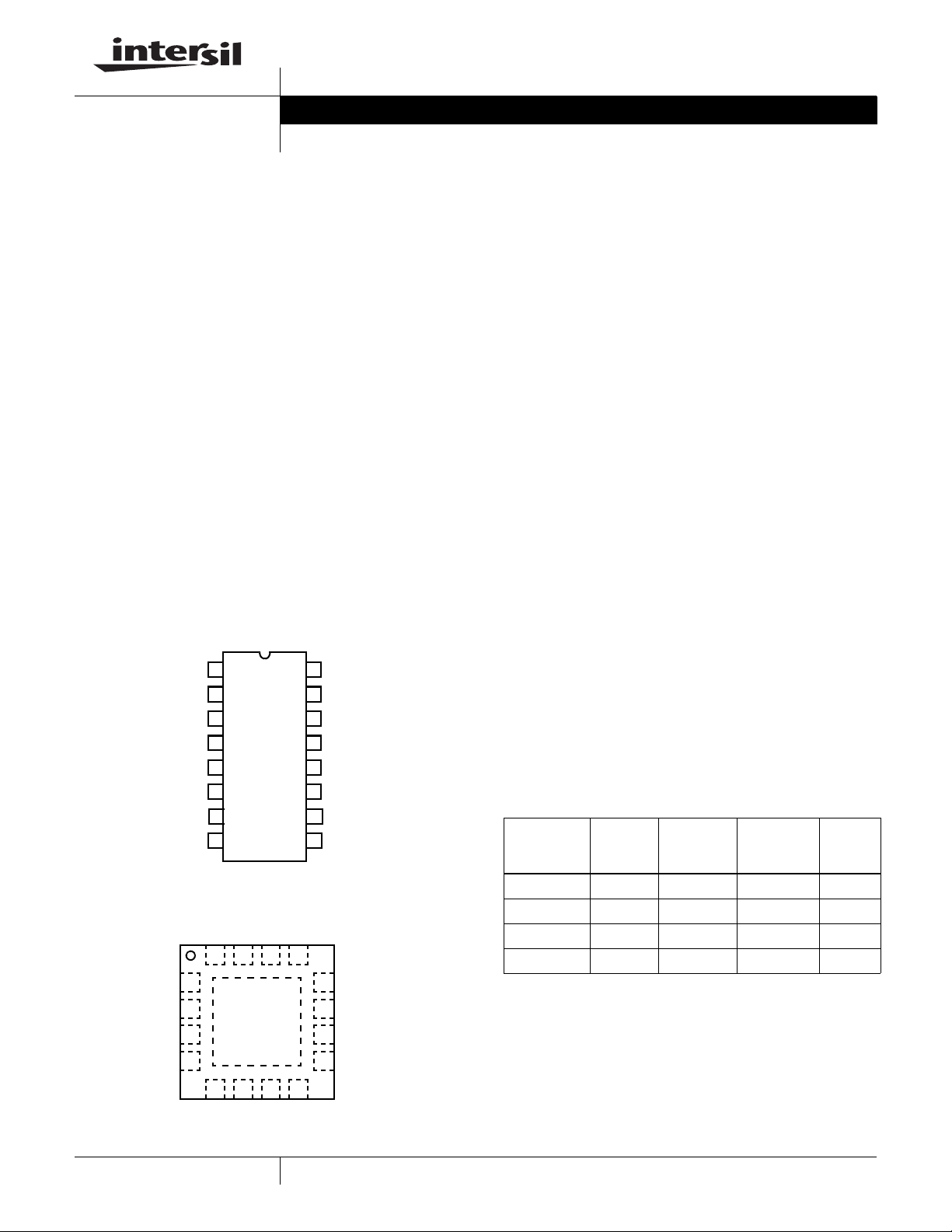
Pinouts
ISL6722A, ISL6723A (16 LD SOIC, TSSOP)
GATE
ISENSE
SYNC/SLEEP
SYNC/SLEEP
SLOPE
UV
OV
1
2
3
SLOPE
4
5
UV
6
OV
7
RTCT
8
ISET
ISL6722A (16 LD QFN)
ISENSE
GATE
15
16 14 13
1
2
3
4
6578
ISET
RTCT
VC
FB
16
15
14
13
12
11
10
9
PGND
12
11
10
9
COMP
VC
PGND
VCC
VREF
LGND
SS
COMP
FB
VCC
VREF
LGND
SS
Features
• 1A MOSFET Gate Driver
• 100µA Start-up Current
• Fast Transient Response with Peak Current Mode Control
• Adjustable Switching Frequency up to 1MHz
• Low Power Sleep Mode (ISL6722A)
• Low Power Shutdown Mode
• Delayed Restart from OV and OC Shutdown Faults
• Adjustable Slope Compensation
• Adjustable Soft-Start
• Adjustable Overcurrent Shutdown Delay
• Adjustable UV and OV Monitors
• Leading Edge Blanking
• 1% Tolerance Voltage Reference
• Pb-Free Plus Anneal Available (RoHS Compliant)
Applications
• Telecom and Datacom Power
• Wireless Base Station Power
• File Server Power
• Industrial Power Systems
• Isolated Buck and Flyback Regulators
• Boost Regulators
Ordering Information
PART
NUMBER*
(Note)
ISL6722AABZ 6722AABZ -40 to +105 16 Ld SOIC M16.15
ISL6723AABZ 6723AABZ -40 to +105 16 Ld SOIC M16.15
ISL6722AAVZ 6722AAVZ -40 to +105 16 Ld TSSOP M16.173
ISL6722AARZ 22AZ -40 to +105 16 Ld QFN L16.3x3B
*Add “-T” suffix to part number for tape and reel packaging.
NOTE: Intersil Pb-free plus anneal products employ special Pb-free
material sets; molding compounds/die attach materials and 100%
matte tin plate termination finish, which are RoHS compliant and
compatible with both SnPb and Pb-free soldering operations. Intersil
Pb-free products are MSL classified at Pb-free peak reflow
temperatures that meet or exceed the Pb-free requirements of
IPC/JEDEC J STD-020.
PART
MARKING
TEMP.
RANGE (°C)
PACKAGE
(Pb-Free)
PKG.
DWG. #
1
CAUTION: These devices are sensitive to electrostatic discharge; follow proper IC Handling Procedures.
1-888-INTERSIL or 1-888-468-3774
| Intersil (and design) is a registered trademark of Intersil Americas Inc.
All other trademarks mentioned are the property of their respective owners.
Copyright © Intersil Americas Inc. 2005, 2007. All Rights Reserved.
Page 2
ISL6722A, ISL6723A
www.BDTIC.com/Intersil
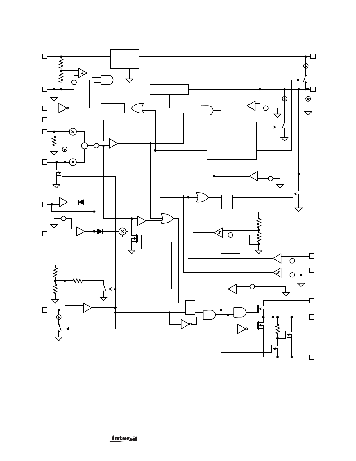
Functional Block Diagram (ISL6722A)
V
CC
LGND
SLEEP
ISET
ISENSE
SLOPE
COMP
VFB
V
REF
START/STOP
UV COMPARATOR
+
-
+
BG
-
0.8
5k
VREF
SS
+
-
+
-
2.5V
53µA
0.1
SS CLAMP
ERROR
AMPLIFIER
+
-
+
S
+
+
-
100mV
ENABLE
RESTART
5V
DELAY
OC DETECT
+
OVERCURRENT
COMPARATOR
COMPARATOR
1/3
PWM
VOLTAGE CLAMP
+
-
100ns
BLANKING
SS CHARGE
SS CHARGED
START
OVERCURRENT
SHUTDOWN
DELAY
FAULT
LATCH
SRQ
SET DOMINANT
VREF
UV COMPARATOR
4.65V
-
+
BG
OC
FAULT
OC
SS LOW
SS LOW
COMPARATOR
Q
-
+
+
-
4.375V
SS DCHG
SS CHGSHTDN
-
+
VREF
SOFT-START
CHARGE
CURRENT
25µA
-
+
-
+
270mV
70µA
ON
ON
VREF
SS
15µA
20k
30k
VREF
3.0V/
12k
1.5V
OSCILLATOR
COMPARATOR
1mA
ON
+
-
-
+
2.50V
-
-
+
BLANKING
ON
+
SRQ
R
Q
COMPARATOR
3.0V
-
+
-
+
36k
+
1.45V
OV
UV
V
C
GATE
PGND
2
FN9237.1
July 11, 2007
Page 3
ISL6722A, ISL6723A
www.BDTIC.com/Intersil
Functional Block Diagram (ISL6723A)
VCC
LGND
ISET
ISENSE
SLOPE
COMP
VFB
VREF
START/STOP
UV COMPARATOR
+
-
+
BG
-
RESTART
0.8
5k
VREF
SS
SS CLAMP
+
-
+
-
2.5V
53µA
0.1
AMPLIFIER
+
S
+
ERROR
+
-
+
-
100mV
5V
1%
ENABLE
DELAY
OC DETECT
+
OVERCURRENT
COMPARATOR
COMPARATOR
1/3
PWM
+
-
BLANKING
SS CHARGE
VOLTAGE CLAMP
START
100nS
SS CHARGED
OVERCURRENT
SHUTDOWN
SET DOMINANT
VREF
UV COMPARATOR
4.65V
-
+
OC
DELAY
FAULT
LATCH
SRQ
Q
FAULT
SS LOW
-
+
BG
OC
SS LOW
COMPARATOR
+
-
-
+
VREF
-
+
4.375V
SS DCHG
SS CHGSHTDN
270mV
SOFT-START
CHARGE
CURRENT
25µA
ON
-
+
70µA
ON
VREF
SS
15µA
RTCT
4V
2V
SYNC
20k
30k
VREF
VREF
3.0V/
1.5V
OSCILLATOR
COMPARATOR
1mA
ON
100
12k
+
-
-
+
2.50V
-
-
+
BLANKING
ON
+
+
-
+
4.5k
BI-DIRECTIONAL
SYNCHRONIZATION
OSC IN
CLK OUT
NO EXT SYNC
EXT SYNC BLANKING
SYNC IN SYNC OUT
VREF
SRQ
Q
COMPARATOR
3.0V
-
+
-
+
+
1.45V
36k
OV
UV
VC
GATE
PGND
3
FN9237.1
July 11, 2007
Page 4
Typical Application - 48V Input Dual Output Flyback, 3.3V @ 2.5A, 1.8V @ 1.0A
www.BDTIC.com/Intersil
P9
VIN+
4
R1
36V TO 75V
C1
R2
R24
C2
C3
C18
C5
CR6
TP1
Q1
T1
ISOLATION
XFMR
CR2
C6
C17
CR5
R21
CR4
C19 C22
SP1 SP2
+
C21
+
R16
U2
C15 C16
+
C20
R17
R19
C14
R18
+3.3V
+1.8V
RETURN
ISL6722A, ISL6723A
R4
VIN-
R25
Q2
D1
TP3
SLEEP
R5
R6
D2
Q3
R8
July 11, 2007
VR1
FN9237.1
R7
TP5
C7
R9
R23
C4
C8
R3
R10
R11
R22
TP2
GATE
ISENSE
SLEEP
SLOPE
UV
OV
RTCT
ISET
R12
U4
ISL6722A
PGND
VCC
VREF
LGND
COMP
VFB
R15
U3
VC
SS
R26
R27
C9
R13
C13
R20
R14
TP4
C12
C11
C10
Page 5
ISL6722A, ISL6723A
www.BDTIC.com/Intersil
Absolute Maximum Ratings Thermal Information
Supply Voltage, V
GATE. . . . . . . . . . . . . . . . . GND -0.3V to Gate Output Limit Voltage
PGND to LGND . . . . . . . . . . . . . . . . . . . . . . . . . . . . . . . . . . . . . . . . ±0.3V
VREF . . . . . . . . . . . . . . . . . . . . . . . . . . . . . . . . . GND - 0.3V to 5.3V
Signal Pins . . . . . . . . . . . . . . . . . . . . . . . . . . . GND - 0.3V to VREF
Peak GATE Current. . . . . . . . . . . . . . . . . . . . . . . . . . . . . . . . . . . .1A
Operating Conditions
Temperature Range
ISL6722AAxZ . . . . . . . . . . . . . . . . . . . . . . . . . .-40°C to +105°C
ISL6723AAxZ . . . . . . . . . . . . . . . . . . . . . . . . . .-40°C to +105°C
Supply Voltage Range (Typical). . . . . . . . . . . . . . . 9VDC to 18VDC
CAUTION: Do not operate at or near the maximum ratings listed for extended periods of time. Exposure to such conditions may adversely impact product reliability and
result in failures not covered by warranty.
NOTES:
is measured in free air with the component mounted on a high effective thermal conductivity test board with “direct attach” features. See
1. θ
JA
Tech Brief TB379.
2. For θ
3. All voltages are with respect to GND.
, the “case temp” location is the center of the exposed metal pad on the package underside.
JC
Electrical Specifications Recommended operating conditions unless otherwise noted. Refer to Block Diagram and Typical Application
UNDERVOLTAGE LOCKOUT
START Threshold (ISL6722A) SLEEP = 0V 7.95 8.25 8.55 V
START Threshold (ISL6723A) 12.4 13.0 13.4 V
STOP Threshold 7.40 7.70 8.20 V
Hysteresis (ISL6722A) 0.50 0.55 1.00 V
Hysteresis (ISL6723A) 4.00 5.00 6.00 V
Start-Up Current, I
OC/OV Fault Operating Current, I
Operating Current, I
Operating Supply Current, I
REFERENCE VOLTAGE
Overall Accuracy Line, load, T
Long Term Stability T
Fault Voltage 4.50 4.65 4.75 V
VREF Good Voltage 4.65 4.80 4.95 V
Hysteresis 75 165 250 mV
Operational Current -10 - - mA
Current Limit -20 - - mA
CURRENT SENSE
Input Impedance -5-kΩ
Offset Voltage 0.08 0.10 0.11 V
Input Voltage Range 0-1.5V
. . . . . . . . . . . . . . . . .GND -0.3V to +20.0V
CC, VC
schematic. 9V < V
Typical values are at T
PARAMETER TEST CONDITIONS MIN TYP MAX UNITS
CC
CC
CC
C
= VC < 20V, Rt = 11kΩ, Ct = 330pF, TA = -40°C to +105°C (Note 4),
CC
= +25°C
A
VCC < START Threshold - 100 175 μA
Includes 1nF GATE loading - 8.0 12.0 mA
Line, load, T
= +125°C, 1000 hours (Note 6) - 5 - mV
A
A
A
Thermal Resistance (Typical) θ
16 Lead QFN (Note 1, 2) . . . . . . . . . . . 52 4
16 Lead SOIC (Note 1) . . . . . . . . . . . . 80 N/A
16 Lead TSSOP (Note 1). . . . . . . . . . . 105 N/A
Maximum Junction Temperature . . . . . . . . . . . . . . .-55°C to +150°C
Maximum Storage Temperature Range. . . . . . . . . .-65°C to +150°C
Pb-free reflow profile . . . . . . . . . . . . . . . . . . . . . . . . . .see link below
http://www.intersil.com/pbfree/Pb-FreeReflow.asp
- 200 300 μA
- 4.5 10.0 mA
= 0°C to +105°C
= -40°C to +105°C
4.95
4.90
5.00
5.00
(°C/W) θJC (°C/W)
JA
5.05
5.05
V
5
FN9237.1
July 11, 2007
Page 6
ISL6722A, ISL6723A
www.BDTIC.com/Intersil
Electrical Specifications Recommended operating conditions unless otherwise noted. Refer to Block Diagram and Typical Application
schematic. 9V < V
Typical values are at T
PARAMETER TEST CONDITIONS MIN TYP MAX UNITS
Blanking Time (Note 6) 30 60 100 ns
Gain, A
CS
ERROR AMPLIFIER
Open Loop Voltage Gain (Note 6) 60 90 - dB
Gain-Bandwidth Product (Note 6) - 15 - MHz
Reference Voltage Initial Accuracy V
Reference Voltage V
COMP to PWM Gain, A
COMP to PWM Offset COMP = 4V 0.51 0.75 0.88 V
FB Input Bias Current V
COMP Sink Current COMP = 1.5V, VFB = 2.7V 2 6 - mA
COMP Source Current COMP = 1.5V, V
COMP VOH V
COMP VOL V
PSRR Frequency = 120Hz (Note 6) 60 80 - dB
SS Clamp, V
OSCILLATOR
Frequency Accuracy 289 318 347 kHz
Frequency Variation with VCC T
Temperature Stability (Note 6) - 8 - %
Maximum Duty Cycle (Note 7) 68 75 81 %
Comparator High Threshold - 3.00 - V
Comparator High Threshold w/Ext. SYNC (ISL6723A) (Note 6) - 4.00 - V
Comparator Low Threshold - 1.50 - V
Discharge Current T
SOFT-START
Charging Current SS = 2V -40 -55 -70 μA
Charged Threshold Voltage 4.26 4.50 4.74 V
Initial Overcurrent Discharge Current Sustained OC Threshold
Overcurrent Shutdown Threshold Voltage Charged Threshold minus,
Fault Discharge Current SS = 2V 0.25 1.0 - mA
Reset Threshold Voltage T
COMP
COMP
= VC < 20V, Rt = 11kΩ, Ct = 330pF, TA = -40°C to +105°C (Note 4),
CC
= +25°C (Continued)
A
V
= 0V, VFB = 2.3V,
SLOPE
= 0.35V, 1.5V
V
ISET
A
= ΔISET/ΔISENSE
CS
= COMP, TA = +25°C (Note 6) 2.465 2.515 2.565 V
FB
= COMP 2.44 2.515 2.590 V
FB
COMP = 4V, TA = +25°C 0.31 0.33 0.35 V/V
= 0V -2 0.1 2 μA
FB
= 2.3V -0.25 -0.5 - mA
FB
= 2.3V 4.25 4.4 5.0 V
FB
= 2.7V 0.4 0.8 1.2 V
FB
SS = 2.5V, VFB = 0V, ISET = 2V 2.4 2.5 2.6 V
= +105°C (f
A
TA = -40°C (f
= 0°C to +105°C
A
T
= -40°C to +105°C
A
< SS < Charged Threshold
= +25°C
T
A
= +25°C 0.22 0.27 0.31 V
A
20V
20V
- f9V)/f
- f9V)/f
9V
9V
0.77 0.79 0.81 V/V
-223
3
0.75
0.70
30 40 55 μA
0.110 0.125 0.140 V
1.0
1.0
1.2
1.2
%
mA
6
FN9237.1
July 11, 2007
Page 7
ISL6722A, ISL6723A
www.BDTIC.com/Intersil
Electrical Specifications Recommended operating conditions unless otherwise noted. Refer to Block Diagram and Typical Application
schematic. 9V < V
Typical values are at T
PARAMETER TEST CONDITIONS MIN TYP MAX UNITS
SLOPE COMPENSATION
Charge Current SLOPE = 2V, T
Slope Compensation Gain Fraction of slope voltage added to
Discharge Voltage V
GATE OUTPUT
Gate Output Limit Voltage V
Gate VOH V
Gate VOL GATE - PGND, IOUT = 150mA
Peak Output Current V
Output “Faulted” Leakage V
Rise Time V
Fall Time V
Minimum ON time ISET = 0.5V; V
OVERCURRENT PROTECTION
Minimum ISET Voltage - - 0.35 V
Maximum ISET Voltage 1.2 - - V
ISET Bias Current V
Restart Delay T
OV AND UV VOLTAGE MONITOR
Overvoltage Threshold 2.4 2.5 2.6 V
Undervoltage Fault Threshold 1.38 1.45 1.52 V
Undervoltage Clear Threshold 1.41 1.53 1.62 V
Undervoltage Hysteresis Voltage 20 50 100 mV
UV Bias Current V
OV Bias Current V
SLEEP (ISL6722A)
SLEEP Input Threshold Voltage Active High 1.4 - 2.7 V
SLEEP Input Current V
@ SLEEP VCC = 15V - 175 210 μA
I
CC
= VC < 20V, Rt = 11kΩ, Ct = 330pF, TA = -40°C to +105°C (Note 4),
CC
= +25°C (Continued)
A
= 0 to +105°C
= -40°C to +105°C
T
A
I
SENSE
Fraction of slope voltage added to
I
SENSE
RTCT
= 20V, C
C
= 0mA
I
OUT
- GATE, VC = 10V,
C
I
= 150mA
OUT
= 20V, C
C
(Note 6)
= 20V, UV = 0V, GATE = 2V 1.2 2.6 - mA
C
= 20V, C
C
1V < GATE < 9V
= 20V, C
C
1V < GATE < 9V
ISENSE to GATE w/10:1 Divider
RTCT = 4.75V through 1kΩ
(Note 6)
= 1.00V -1.0 - 1.0 μA
ISET
= +25°C 150 295 445 ms
A
= 2.00V -1.0 - 1.0 μA
UV
= 2.00V -1.0 - 1.0 μA
OV
SLEEP
A
, TA = +25°C
(Note 4)
= 4.5V - 0.1 0.2 V
= 1nF,
GATE
IOUT = 10mA
= 1nF
GATE
= 1nF
GATE
= 1nF
GATE
= 0V; VC = 11V
FB
= 4.0V 11 25 46 μA
-45
-41
0.097 - 0.103 V/V
0.082 - 0.118 V/V
11.0 13.5 16.0 V
-1.52.2V
-1.2
-1.0- A
-60100ns
-1540ns
--110ns
-53
-53
0.6
-65
-65
1.5
0.8
μA
V
7
FN9237.1
July 11, 2007
Page 8
ISL6722A, ISL6723A
www.BDTIC.com/Intersil
Electrical Specifications Recommended operating conditions unless otherwise noted. Refer to Block Diagram and Typical Application
schematic. 9V < V
Typical values are at T
PARAMETER TEST CONDITIONS MIN TYP MAX UNITS
SYNCHRONIZATION (ISL6723A)
Input High Threshold --2.5V
Input Pulse Width 25 - - ns
Input Frequency Range (Note 6) 0.65 x Free
Input Impedance -4.5-kΩ
VOH R
VOL R
SYNC Advance SYNC rising edge to GATE falling
Output Pulse Width C
NOTES:
4. Specifications at -40°C and +105°C are guaranteed by +25°C test with margin limits.
5. This is the V
current consumed when the device is active but not switching. Does not include gate drive current.
CC
6. Limits should be considered typical and are not production tested.
7. This is the maximum duty cycle achievable using the specified values of RT and CT . Larger or smal ler maximum duty cycles may be obtained
using other values for RT and CT. See Equations 1 through 4.
= VC < 20V, Rt = 11kΩ, Ct = 330pF, TA = -40°C to +105°C (Note 4),
CC
= +25°C (Continued)
A
-1.0MHz
Running
= 4.5kΩ 2.5 - - V
LOAD
= open - - 0.1 V
LOAD
-2555ns
edge, C
SYNC
= C
GATE
= 100pF 50 - - ns
SYNC
= 100pF
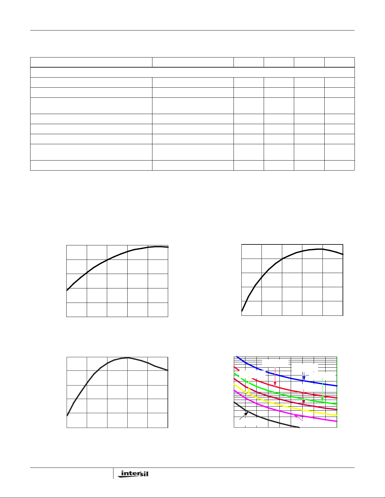
Typical Performance Curves
1.002
1.000
0.998
0.995
0.993
NORMALIZED EA REFERENCE
0.991
-40 -10 20 50 80 110
TEMPERATURE (°C)
FIGURE 1. EA REFERENCE VOLTAGE vs TEMPERATURE
1.002
0.996
0.989
0.983
0.976
NORMALIZED FREQUENCY
0.970
-40 -10 20 50 80 110
TEMPERATURE (°C)
1.002
1.000
0.998
0.995
0.993
NORMALIZED VREF
0.991
FIGURE 2. V
1000
100
FREQUENCY (kHz)
10
10 20 30 40 50 60 70 80 90 100
-40 -10 20 50 80 110
REFERENCE VOLTAGE vs TEMPERATURE
REF
CT = 680pF
CT = 2200pF
TEMPERATURE (°C)
CT = 220pF
RT (kΩ)
CT = 100pF
CT = 330pF
CT = 470pF
CT = 1000pF
FIGURE 3. OSCILLATOR FREQUENCY vs TEMPERATURE FIGURE 4. CAPACITANCE vs FREQUENCY
8
FN9237.1
July 11, 2007
Page 9

ISL6722A, ISL6723A
www.BDTIC.com/Intersil
Pin Descriptions
SLOPE - Means by which the ISENSE ramp slope may be
increased for improved noise immunity or improved control
loop stability for duty cycles greater than 50%. An internal
current source charges an external capacitor to GND during
each switching cycle. The resulting ramp is scaled and
added to the ISENSE signal.
SLEEP (ISL6722A) - A logic level control input that disables
the IC and activates the low power standby mode. SLEEP is
active high.
SYNC (ISL6723A) - A bidirectional synchronization signal
used to coordinate the switching frequency of multiple units.
Synchronization may be achieved by connecting the SYNC
signal of each unit together or by using an external master
clock signal. The oscillator timing capacitor, C
required, even if an external clock is used. The first unit to
assert this signal assumes control.
RTCT - This is the oscillator timing control pin. The
operational frequency and maximum duty cycle are set by
connecting a resistor, R
timing capacitor, C
, between V
T
, from this pin to LGND. The oscillator
T
REF
produces a sawtooth waveform with a programmable
frequency range of 100kHz to 1.0MHz. The charge time, t
the discharge time, t
, the switching frequency, fsw, and the
D
maximum duty cycle, Dmax, can be calculated from the
Equations 1, 2, 3 and 4:
tC0.655 RTCT••≈ S
, is still
T
and this pin and a
C
(EQ. 1)
OV - Overvoltage monitor input pin. This signal is compared
to an internal 2.5V reference to detect an overvoltage
condition.
UV - Undervoltage monitor input pin. This signal is
compared to an internal 1.45V reference to detect an
undervoltage condition.
ISENSE - This is the input to the current sense comparators.
The IC has two current sensing comparators, a PWM
comparator for peak current mode control, and an
overcurrent protection comparator. The overcurrent
comparator threshold is adjustable through the ISET pin.
Exceeding the overcurrent threshold will start a delayed
shutdown sequence. Once an overcurrent condition is
detected, the soft-start charge current source is disabled and
a discharge current source is enabled. The soft-start
capacitor begins discharging, and if it discharges to less than
4.375V (sustained overcurrent threshold), a shutdown
condition occurs and the GATE output is forced low. At this
point a reduced discharge current takes over until the
soft-start voltage reaches 0.27V (Reset Threshold). The
GATE output remains low until the reset threshold is
attained. At this point a soft-start cycle begins.
,
If the overcurrent condition ceases, and then an additional
50µs period elapses before the shutdown threshold is
reached, no shutdown occurs and the soft-start voltage is
allowed to recharge.
LGND - LGND is a small signal reference ground for all
analog functions on this device.
t
RT– CTLN
D
1
---------------------
= Hz
f
sw
Dmax t
T
DTC
+
Cfsw
-------------------------------------------
••≈ S
⎝⎠
0.001 RT1.9–•
•=
(EQ. 2)
(EQ. 3)
(EQ. 4)
0.001 RT3.6–•
⎛⎞
Figure 4 may be used as a guideline in selecting the
capacitor and resistor values required for a given frequency.
COMP - COMP is the output of the error amplifier and the
input of the PWM comparator. The control loop frequency
compensation network is connected between the COMP and
FB pins.
The ISL6722A, ISL6723A feature a built-in full cycle
soft-start. Soft-start is implemented as a clamp on the
maximum COMP voltage.
FB - Feedback voltage input connected to the inverting input
of the error amplifier. The non-inverting input of the error
amplifier is internally tied to a reference voltage.
PGND - This pin provides a dedicated ground for the output
gate driver. The LGND and PGND pins should be connected
externally using a short printed circuit board trace close to
the IC. This is imperative to prevent large, high frequency
switching currents from flowing through the ground
metallization inside the IC. (Decouple V
to PGND with a
C
low ESR 0.1µF or larger capacitor.)
GATE - This is the device output. It is a high current power
driver capable of driving the gate of a power MOSFET with
peak currents of 1.0A. This GATE output is actively held low
when V
is below the UVLO threshold.
CC
The output high voltage is clamped to ~ 13.5V. Voltages
exceeding this clamp value should not be applied to the
GA TE pin. The output stage provides very low impedance to
overshoot and undershoot.
V
- This pin is for separate collector supply to the output
C
gate drive. Separate V
and PGnd helps decouple the IC’s
C
analog circuitry from the high power gate drive noise.
(Decouple V
to PGND with a low ESR 0.1µF or larger
C
capacitor.)
V
- VCC is the power connection for the device. Although
CC
quiescent current, I
, is low, it is dependent on the
CC
frequency of operation. To optimize noise immunity, bypass
9
FN9237.1
July 11, 2007
Page 10

ISL6722A, ISL6723A
www.BDTIC.com/Intersil
VCC to LGND with a ceramic capacitor as close to the VCC
and LGND pins as possible.
The total supply current (I
depending on the load applied to GATE. Total current is the
sum of the quiescent current and the average gate current.
Knowing the operating frequency, f
gate charge, Qg, the average GATE output current can be
calculated from Equation 5:
Igate Qg f
VREF - The 5.00V reference voltage output. Bypass to
LGND with a 0.01µF or larger capacitor to filter this output as
needed. Using capacitance less than this value may result in
unstable operation.
SS - Connect the soft-start capacitor between this pin and
LGND to control the duration of soft-start. The value of the
capacitor determines both the rate of increase of the duty
cycle during start up, and also controls the overcurrent
shutdown delay.
ISET - A DC voltage between 0.35V and 1.2V applied to this
input sets the pulse-by-pulse overcurrent threshold. When
overcurrent inception occurs, the SS capacitor begins to
discharge and starts the overcurrent delayed shutdown
cycle.
•= A
sw
plus ICC) will be higher,
C
, and the MOSFET
sw
(EQ. 5)
Functional Description
Features
The ISL6722A and ISL6723A current mode PWMs make an
ideal choice for low-cost flyback and forward topology
applications requiring enhanced control and supervisory
capability . With adjustable over and undervoltage thresholds,
overcurrent threshold, and hiccup delay, a highly flexible
design with minimal external components is possible. Other
features include peak current mode control, adjustable softstart, slope compensation, adjustable oscillator frequency,
and a low power sleep mode.
Oscillator
The ISL6722A and ISL6723A have a sawtooth oscillator with
a programmable frequency range to 1MHz, which can be
programmed with a resistor and capacitor on the RTCT pin.
(Please refer to Figure 4 for the resistance and capacitance
required for a given frequency.)
Implementing Synchronization (ISL6723A)
The oscillator can be synchronized to an external clock
applied at the SYNC pin or by connecting the SYNC pins of
multiple ICs together. If an external master clock signal is
used, it must be at least 65% of the free running frequency of
the oscillator for proper synchronization. The external
master clock signal should have a pulse width greater than
20ns. If no master clock is used, the first device to assert
SYNC assumes control of the SYNC signal. An external
SYNC pulse is ignored if it occurs during the first 1/3 of the
switching cycle.
During normal operation the RTCT voltage charges from
1.5V to 3.0V and back during each cycle. Clock and SYNC
signals are generated when the 3.0V threshold is reached. If
an external clock signal is detected during the latter 2/3 of
the charging cycle, the oscillator switches to external
synchronization mode and relies upon the external SYNC
signal to terminate the oscillator cycle. The generation of a
SYNC signal is inhibited in this mode. If the RTCT voltage
exceeds 4.0V (i.e. no external SYNC signal terminates the
cycle), the oscillator reverts to the internal clock mode and a
SYNC signal is generated.
Soft-Start Operation
The ISL6722A and ISL6723A feature a soft-start using an
external capacitor in conjunction with an internal current
source. Soft-start is used to reduce voltage stresses and
surge currents during start up.
Upon start up, the soft-start circuitry clamps the error
amplifier output (COMP pin) to a value proportional to the
soft-start voltage. The error amplifier output rises as the
soft-start capacitor voltage rises. This has the effect of
increasing the output pulse width from zero to the steady
state operating duty cycle during the soft-start period. When
the soft-start voltage exceeds the error amplifier voltage,
soft-start is completed. Soft-start forces a controlled output
voltage rise. Soft-start occurs during start-up and after
recovery from a fault condition or overcurrent shutdown. The
soft-start voltage is clamped to 4.5V.
Gate Drive
The output of these controllers is capable of sourcing and
sinking 1A peak current. Separate collector supply (V
power ground (PGnd) pins help isolate the IC’s analog
circuitry from the high power gate drive noise. T o limit the
peak current through the IC, an external resistor may be
placed between the totem-pole output of the IC (GATE pin)
and the gate of the MOSFET. This small series resistor also
damps any oscillations caused by the resonant tank of the
parasitic inductances in the traces of the board and the
FET’s input capacitance.
) and
C
Slope Compensation
For applications where the maximum duty cycle is less than
50%, slope compensation may be used to improve noise
immunity, pa rticularly at lighter loads. The amount of slope
compensation required for noise immunity is determined
empirically, but is generally about 10% of the full scale
current feedback signal. For applications where the duty
cycle is greater than 50%, slope compensation is required to
prevent instability. Slope compensation is a technique in
which the current feedback signal is modified by adding
additional slope to it.
10
FN9237.1
July 11, 2007
Page 11

ISL6722A, ISL6723A
www.BDTIC.com/Intersil
The minimum amount of slope compensation required
corresponds to 1/2 the inductor downslope. However, adding
excessive slope compensation results in a control loop that
behaves more as a voltage mode controller than as current
mode controller.
DOWNSLOPE
Downslope
CURRENT SENSE SIGNAL
Current Sense Signal
ISENSE Signal (V)
ISENSE SIGNAL (V)
TIME
Time
FIGURE 5.
The minimum amount of capacitance to place at the SLOPE
pin is:
Cslope 4.246–×10
where t
is the On time and Vslope is the amount of
ON
ON
--------------------
•= F
Vslope
(EQ. 6)
t
voltage to be added as slope compensation to the current
feedback signal. In general, the amount of slope
compensation added is 2 to 3 times the minimum required.
be shown that the naturally-sampled modulator gain, Fm,
without slope compensation, is Equation 9:
1
-------------------- -
Fm
=
⋅
Sn t
sw
where Sn is the slope of the sawtooth signal and t
sw
(EQ. 9)
is the
switching frequency. When an external ramp is added, the
modulator gain becomes Equation 10:
1
----------------------------------- -
Fm
==
Sn Se+()t
sw
1
-------------------------
Snt
m
c
sw
(EQ. 10)
where Se is slope of the external ramp.
Se
m
-------
1
+=
c
Sn
(EQ. 11)
The criteria for determining the correct amount of external
ramp can be determined by appropriately setting the
damping factor of the double-pole located at half the
oscillator frequency. The double-pole will be critically
damped if the Q-factor is set to 1, under-damped for Q > 1,
and over-damped for Q < 1. An under-damped condition
may result in current loop instability.
-------------------------------------------------
=
Q
π m
c
1
1D–()0.5–()
(EQ. 12)
Example:
Assume the inductor current signal presented at the ISENSE
pin decreases 125mV during the Off period, and:
Switching Frequency, f
= 250kHz
sw
Duty Cycle, D = 60%
tON = D/fsw = 0.6/250E3 = 2.4µs
= (1 - D)/fsw = 1.6µs
t
OFF
Determine the downslope:
Downslope = 0.125V/1.6µs = 78mV/µs. Now determine the
amount of voltage that must be added to the current sense
signal by the end of the On time.
1
Vslope
-- -
0.078 2.4•• 94mV==
2
(EQ. 7)
Therefore,
Cslope min()4.24
×10
6–
• 110pF≈=
×10
2.4
-----------------------
0.094
6–
(EQ. 8)
The value calculated, 110pF, represents the minimum slope
compensation required. An appropriate slope compensation
capacitance for this example would be 1/2 to 1/3 the
calculated value, or between 68pF and 33pF.
A more rigorous treatment of slope compensation can be
obtained from the small signal current-mode model [1]. It can
where D is the maximum duty cycle. Setting Q = 1 and
solving for S
S
=
eSn
yields:
e
1
⎛⎞
⎛⎞
-- -
⎝⎠
⎝⎠
π
1
-------------
0.5+
1D–
1–
(EQ. 13)
Since Sn and Se are the on time slopes of the current ramp
and the external ramp, respectively , they can be multiplied
by t
to obtain the voltage change that occurs during tON.
ON
1
⎛⎞
⎛⎞
V
eVn
where V
-- -
=
⎝⎠
⎝⎠
π
is the change in the current feedback signal during
n
the on time and V
1
-------------
0.5+
1–
1D–
is the voltage that must be added by the
e
(EQ. 14)
external ramp.
For buck-derived topologies, V
can be solved for in terms of
n
output voltage, current transducer components, and output
inductance yielding:
tSWV⋅ORCS⋅
----------------------------------------
V
= V
e
N
⋅
CTLO
where R
is the current sense burden resistor, N
CS
current transformer turns ratio, L
V
is the output voltage, and Ns and Np are the secondary
O
N
1
S
⎛⎞
------- -
-- -
⋅
D0.5–+
⎝⎠
N
π
P
is the output inductance,
O
(EQ. 15)
CT
is the
and primary turns, respectively.
11
FN9237.1
July 11, 2007
Page 12

ISL6722A, ISL6723A
www.BDTIC.com/Intersil
For flyback topologies, Vn can be solved for in terms of
output voltage, current transducer components, and primary
inductance yielding:
tSWV⋅ORCS⋅
----------------------------------------
V
= V
e
where R
⋅
N
CTLP
is the current sense burden resistor, N
CS
current transformer turns ratio, L
V
is the output voltage, and NS and NP are the secondary
O
N
1
P
⎛⎞
------- -
-- -
⋅
D0.5–+
⎝⎠
N
π
S
is the primary inductance,
P
(EQ. 16)
CT
is the
and primary turns, respectively. If a curre nt transformer is not
used, then N
CT
= 1.
For discussion purposes, only the flyback topology will be
further discussed. A discussion addressing the buck derived
topologies may be found in the datasheet for the ISL6753.
The current sense signal, which represents the primary
current after it has been reflected through the current sense
transformer and passed through the current sense burden
resistor, is:
2L
t⋅⋅
SW
N
P
------- -
⋅+
N
S
(EQ. 17)
O
P
R
⎛⎞
⎛⎞
CS
----------- -
I
= V
V
CS
N
where V
and I
CS
is the output current at current limit.
O
⋅
⎜⎟
⎜⎟
O
⎝⎠
⎝⎠
CT
is the voltage across the current sense resistor
1D–()V
N
S
------- -
----------------------------------------------
N
P
Since the peak current limit threshold is determined by ISET,
the total current feedback signal plus the external ramp
voltage must sum to this value when the output load is at the
current limit threshold.
V
eVCS
0.8⋅()0.100++ISET=
(EQ. 18)
where the internal gain and offset voltages of the IC have
been included. Substituting Equations 15 and 17 into
Equation 18 and solving for R
⋅⋅
⋅
ISET 0.1–()NCT⋅
1
⎛⎞
-- -
⋅ 0.8I
⎝⎠
π
-----------------------------------------------------------------------------------------------------------------------
R
= Ω
CS
T
SWVONP
------------------------------------- -
L
PNS
yields
CS
N
S
0.6D 0.1–+
------- -
⋅+
O
N
P
(EQ. 19)
Adding slope compensation is accomplished in the
ISL6722A, ISL6723A using the SLOPE input. The value of
Ve determined in Equation 16, multiplied 10x, is the voltage
required at the SLOPE input.
C
SLOPE
I
-----------------------------------
=
⋅
SLOPEtON
V
10⋅
e
(EQ. 20)
voltage falls outside of the user designated operating range,
a shutdown fault occurs. For OV faults, the supply current,
I
, is reduced to 200µA for ~ 295ms at which time recovery
CC
is attempted. If the fault is cleared, a soft-start cycle begins.
Otherwise another shutdown cycle occurs. A UV condition
also results in a shutdown fault, but the device does not
enter the low power mode and no restart delay occurs when
the fault clears.
A resistor divider between Vin and LGND to each input
determines the operational thresholds. The UV threshold
has a fixed hysteresis of 75mV nominal.
Overcurrent Operation
The overcurrent threshold level is set by the voltage applied
at the ISET pin. Setting the overcurrent level may be
accomplished by using a resistor divider network from VREF
to LGND. The ISET threshold should be set at a level that
corresponds to the desired peak output inductor current plus
the additive effects of slope compensation.
Overcurrent delayed shutdown is enabled once the soft-start
cycle is complete. If an overcurrent condition is detected, the
soft-start charging current source is disabled and the
discharging current source is enabled. The soft-start
capacitor is discharged at a rate of 40µA. At the same time a
50µs retriggerable one-shot timer is activated. It remains
active for 50µs after the overcurrent condition stops. The
soft-start discharge cycle cannot be reset until the one-shot
timer becomes inactive. If the soft-start capacitor discharges
by more then 0.125V to 4.375V, the output is disabled and
the soft-start capacitor is discharged. The output remains
disabled and I
A new soft-start cycle is then initiated. The shutdown and
restart behavior of the OC protection is often referred to as
hiccup operation due to its repetitive start-up and shutdown
characteristic.
If the overcurrent condition ceases at least 50µs prior to the
soft-start voltage reaching 4.375V, the soft-start charging
and discharging currents revert to normal operation and the
soft-start voltage is allowed to recover.
Hiccup OC protection may be defeated by setting ISET to a
voltage that exceeds the Error Amplifier current control
voltage, or about 1.5V.
drops to 200µA for approximately 295ms.
CC
where I
is the internal charging current on SLOPE,
SLOPE
nominally 53µA.
Over and Undervoltage Monitor
The OV and UV signals are inputs to a window comparator
used to monitor the input voltage level to the converter. If the
12
FN9237.1
July 11, 2007
Page 13

ISL6722A, ISL6723A
www.BDTIC.com/Intersil
Figure 6 depicts overcurrent behavior during soft-start.
ISENSE’ represents the scaled values of ISENSE at the
input to the overcurrent comparator.
4.5 V
SS
ISET
ISENSE
TE
GA
FIGURE 6. PULSE-BY-PULSE OC BEHAVIOR DURING SS
Although an overcurrent condition exists, a shutdown is not
allowed prior to completion of the SS cycle. Only peak
current limit operates during the soft-start cycle. If the
overcurrent condition were to continue beyond the soft-start
cycle, a delayed overcurrent shutdown would occur as
shown in Figure 7:
4.375V
GND
4.5 V
295ms
SS
ISET
ISENSE'
GATE
FIGURE 7. OC SHUTDOWN BEHAVIOR
If the overcurrent condition is removed prior to a shutdown, a
recovery can occur as indicated in Figure 8. When the load
decreases below the overcurrent threshold and an additional
50µs elapses without the SS dropping below 4.375V, the
overcurrent circuitry resets and the soft-start voltage
recovers.
OC
4.5V
50ms
SS
4.375V
ISET
ISENSE'
GATE
FIGURE 8. OC RECOVERY PRIOR TO SHUTDOWN
Leading Edge Blanking
The initial 100ns of the current feedback signal input at
ISENSE is removed by the leading edge blanking circuitry.
The blanking period begins when the GATE output leading
edge exceeds 3.0V . Leading edge blanking prevents current
spikes from parasitic elements in the power supply from
causing false trips of the PWM comparator and the
overcurrent comparator.
Fault Conditions
A Fault condition occurs if VREF falls below 4.65V, the OV
input exceeds 2.50V, or the UV input falls below 1.45V.
When a Fault is detected, the GATE output is disabled and
the soft-start capacitor is quickly discharged. When the Fault
condition clears and the soft-start voltage is below the reset
threshold, a soft-start cycle begins.
Ground Plane Requirements
Careful layout is essential for satisfactory operation of the
device. A good ground plane must be employed. A unique
section of the ground plane must be designated for high di/dt
currents associated with the output stage. Power ground
(PGND) can be separated from the logic ground (LGND) and
connected at a single point. V
should be bypassed directly
C
to PGND with good high frequency capacitors. The return
connection for input power and the bulk input capacitor
should be connected to the PGND ground plane.
Reference Design
The Typical Application Schematic features the ISL6722A in
a conventional dual output 10W discontinuous mode flyback
DC/DC converter. The ISL6722AEVAL1 demonstration unit
implements this design and is available for evaluation.
The input voltage range is from 36 to 75V DC, and the two
outputs are 3.3V @ 2.5A and 1.8V @ 1.0A. Cross regulation
is achieved using the weighted sum of the two outputs.
Circuit Element Descriptions
The converter design may be broken down into the following
functional blocks:
Input Storage and Filtering Capacitance: C
Isolation Transformer: T1
Primary voltage Clamp: CR6, R24, C
Start Bias Regulator: R1, R2, R6, Q3, V
Operating Bias and Regulator: R25, Q2, D1, C5, CR2, D
Main MOSFET Power Switch: Q
1
Current Sense Network: R4, R3, R23, C
Feedback Network:, R13, R15, R16, R17, R18, R19, R20,
R
, R27, C13, C14, U2, U
26
3
Control Circuit: C7, C8, C9, C10, C11, C12, R5, R6, R8, R9,
R10, R11, R12, R14, R
22
Output Rectification and Filtering: CR4, CR5, C15, C16, C19,
C
, C21, C
20
Secondary Snubber: R21, C
22
17
18
R1
4
, C2, C
1
3
2
13
FN9237.1
July 11, 2007
Page 14

ISL6722A, ISL6723A
www.BDTIC.com/Intersil
Design Criteria
The following design requirements were selected:
Switching Frequency, fsw: 200kHz
VIN: 36V to 75V
V
V
V
P
Efficiency: 70%
Maximum Duty Cycle, Dmax: 0.45
Transformer Design
The design of a flyback transformer is a non-trivial affair. It is
an iterative process which requires a great deal of
experience to achieve the desired result. It is a process of
many compromises, and even experienced designers will
produce different designs when presented with identical
requirements. The iterative design process is not presented
here for clarity.
The abbreviated design process follows:
• Select a core geometry suitable for the application.
• Select suitable core material(s).
• Select maximum flux density desired for operation.
• Select core size. Core size will be dictated by the
• Determine maximum desired flux density. Depending on
• Determine the number of primary turns.
• Determine the turns ratio.
• Select the wire gauge for each winding.
• Determine winding order and insulation requirements.
• Verify the design.
: 3.3V @ 2.5A
OUT(1)
: 1.8V @ 1.0A
OUT(2)
OUT(Bias)
OUT
: 12V @ 50mA
: 10W
Constraints of height, footprint, mounting preference, and
operating environment will affect the choice.
capability of the core structure to store the required
energy, the number of turns that have to be wound, and
the wire gauge needed. Often the window area (the space
used for the windings) and power loss determine the final
core size. For flyback transformers, the ability to store
energy is the critical factor in determining the core size.
The cross sectional area of the core and the length of the
air gap in the magnetic path determine the energy storage
capability.
the frequency of operation, the core material selected, and
the operating environment, the allowed flux density must
be determined. The decision of what flux density to allow
is often difficult to determine initially. Usually the highest
flux density that produces an acceptable design is used,
but often the winding geometry dictates a larger core than
is required based on flux density and energy storage
calculations.
Input Power:
/Efficiency = 14.3W (use 15W)
P
OUT
Max On Time: t
ON(max)
= Dmax/fsw = 2.25µs
Average Input Current: Iavg(in) = Pin/Vin(min) = 0.42A
Peak Primary Current:
Ippk
-------------------------------------------
fsw t
ON
max()•
1.87==A
(EQ. 21)
2Iavgin()•
Maximum Primary Inductance:
Lp max()
Vin min()t
-----------------------------------------------------------
Ippk
ON
max()•
43.3==μH
(EQ. 22)
Choose desired primary inductance to be 40µH.
The core structure must be able to deliver a certain amount
of energy to the secondary on each switching cycle in order
to maintain the specified output power.
ΔwPout
•= joules
---------------------------------
Fsw Vout•
(EQ. 23)
Vout Vd+〈〉
where Δw is the amount of energy required to be transferred
each cycle and Vd is the drop across the output rectifier.
The capacity of a gapped ferrite core structure to store
energy is dependent on the volume of the airgap and can be
expressed as:
Δw••
2 μ
o
== m
Vg Aeff lg•
-----------------------------
2
ΔB
3
(EQ. 24)
where Aeff is the effective cross sectional area of the core in
2
m
, lg is the length of the airgap in meters, µo is the
permeability of free space (4π • 10
-7
), and ΔB is the change
in flux density in Tesla.
A core structure having less airgap volume than calculated
will be incapable of providing the full output power over
some portion of its operating range. On the other hand, if the
length of the airgap becomes large, magnetic field fringing
around the gap occurs. This has the effect of increasing the
airgap volume. Some fringing is usually acceptable, but
excessive fringing can cause increased losses in the
windings around the gap resulting in excessive heating.
Once a suitable core and gap combination are found, the
iterative design cycle begins. A design is developed and
checked for ease of assembly and thermal performance. If
the core does not allow adequate space for the windings,
then a core with a larger window area is required. If the
transformer runs hot, it may be necessary to lower the flux
density (more primary turns, lower operating frequency),
select a less lossy core material, change the geometry of the
windings (winding order), use heavier gauge wire or multifilar windings, and/or change the type of wire used (Litz wire,
for example).
14
FN9237.1
July 11, 2007
Page 15

ISL6722A, ISL6723A
www.BDTIC.com/Intersil
For simplicity, only the final design is further described.
An EPCOS EFD 20/10/7 core using N87 material gapped to
an A
value of 25 nH/N2 was chosen. It has more than the
L
required air gap volume to store the energy required, but
was needed for the window area it provides.
-6
Aeff = 31 • 10
m
2
lg = 1.56 • 10-3 m
The flux density ΔB is only 0.069T or 690 gauss, a relatively
low value.
2
μoN
----------------------------------------
L
= μH
p
Aeff••
p
lg
(EQ. 25)
Since the number of primary turns, Np, may be calculated.
The result is N
= 40 turns. The secondary turns may be
p
calculated in Equation 26:
Ig Vout Vd+〈〉Tr••
-------------------------------------------------------- -
≤
N
s
Ippk μoAeff•••
N
p
(EQ. 26)
where Tr is the time required to reset the core. Since
discontinuous MMF mode operation is desired, the core
must completely reset during the off time. To maintain
discontinuous mode operation, the maximum time allowed to
reset the core is t
sw
- t
ON(max)
where tsw = 1/fsw. The
minimum time is application dependent and at the designers
discretion knowing that the secondary winding RMS current
and ripple current stress in the output capacitors increases
with decreasing reset time. The calculation for maximum N
for the 3.3V output using T = t
sw
- t
ON (max)
= 2.75µs is 5.52
turns.
The determination of the number of secondary turns is also
dependent on the number of outputs and the required turns
ratios required to generate them. If schottky output rectifiers
are used and we assume a forward voltage drop of 0.45V,
the required turns ratio for the two output voltages, 3.3V and
1.8V, is 5:3.
With a turns ratio of 5:3 for the secondary windings, we will
use N
= 5 turns and Ns2 = 3 turns. Checking the reset time
s1
using these values for the number of secondary turns yields
a duration of Tr = 2.33µs or about 47% of the switching
period, an acceptable result.
The bias winding turns may be calculated similarly, only a
diode forward drop of 0.7V is used. The rounded off result is
17 turns for a 12V bias.
The next step is to determine the wire gauge. The RMS
current in the primary winding may be calculated in
Equation 27:
t
Ip rms()Ippk
ON max()
-------------------------•= A
3tsw•
(EQ. 27)
The peak and RMS current values in the remaining windings
may be calculated in Equation 28:
2Ioutt
••
----------------------------------
Ispk
= A
Tr
Irms 2 Iout•
sw
t
sw
-------------- -•= A
3Tr•
(EQ. 28)
(EQ. 29)
The RMS current for the primary winding is 0.72A, fo r the
3.3V output, 4.23A, for the 1.8V output, 1.69A, and for the
bias winding, 85mA.
T o minimize the transformer leakage inductance, the primary
was split into two sections connected in parallel and
positioned such that the other windings were sandwiched
between them. The output windings were configured so that
the 1.8V winding is a tap off of the 3.3V winding. Tapping the
1.8V output requires that the shared portion of the
secondary conduct the combined current of both outputs.
The secondary wire gauge must be selected accordingly.
The determination of current carrying capacity of wire is a
compromise between performance, size, and cost. It is
affected by many design constraints such as operating
frequency (harmonic content of the waveform) and the
winding proximity/geometry. It generally ranges between
250 and 1000 circular mils per ampere. A circular mil is
defined as the area of a circle 0.001” (1 mil) in diameter. As
the frequency of operation increases, the AC resistance of
s
the wire increases due to skin and proximity effects. Using
heavier gauge wire may not alleviate the problem. Instead
multiple strands of wire in parallel must be us ed . In some
cases Litz wire is required.
The winding configuration selected is:
Primary #1: 40T, 2 #30 bifilar
Secondary: 5T, 0.003” (3 mil) copper foil tapped at 3T
Bias: 17T #32
Primary #2: 40T, 2 #30 bifilar
The internal spacing and insulation system was designed for
1500 VDC dielectric withstand rating between the primary
and secondary windings.
Power MOSFET Selection
Selection of the main switching MOSFET requires
consideration of the voltage and current stresses that will be
encountered in the application, the power dissipated by the
device, its size, and its cost.
The input voltage range of the converter is 36VDC to
75VDC. This suggests a MOSFET with a voltage rating of
150V is required due to the flyback voltage likely to be seen
on the primary of the isolation transformer.
15
FN9237.1
July 11, 2007
Page 16

ISL6722A, ISL6723A
www.BDTIC.com/Intersil
The losses associated with MOSFET operation may be
divided into three categories: conduction, switching, and
gate drive.
The conduction losses are due to the MOSFET’s ON
resistance.
Ippk
Pcond r
where r
DS(ON)
DS ON()
is the ON resistance of the MOSFET and
2
Iprms
•= W
(EQ. 30)
Iprms is the RMS primary current. Determining the
conduction losses is complicated by the variation of r
DS(ON)
with temperature. As junction temperature increases, so
does r
, which increases losses and raises the
DS(ON)
junction temperature more, and so on. It is possible for the
device to enter a thermal runaway situation without proper
heatsinking. As a general rule of thumb, doubling the +25°C
r
specification yields a reasonable value for
DS(ON)
estimating the conduction losses at +125°C junction
temperature.
The switching losses have two components, capacitive
switching losses and voltage/current overlap losses. The
capacitive losses occur during turn on of the device and may
be calculated as follows:
Pswcap
1
-- -
Cfet Vin
2
2
fsw•••= W
(EQ. 31)
where Cfet is the equivalent output capacitance of the
MOSFET. Device output capacitance is specified on
datasheets as Coss and is non-linear with applied voltage.
To find the equivalent di screte capacitance, Cfet, a charge
model is used. Using a known current source, the time
required to charge the MOSFET drain to the desired
operating voltage is determined and the equivalent
capacitance may be calculated in Equation 32.
Ichg t•
------------------- -
Cfet
= F
V
(EQ. 32)
The other component of the switching loss is due to the
overlap of voltage and current during the switching
transition. A switching transition occurs when the MOSFET
is in the process of either turning on or off. Since the load is
inductive, there is no overlap of voltage and current during
the turn on transition, so only the turn off transition i s of
significance. The power dissipation may be estimated as
Equation 33:
Psw
1
-- -
Ippk• Vin Tol f
x
•••≈
sw
(EQ. 33)
where Tol is the duration of the overlap period and x ranges
from about 3 to 6 in typical applications and depends on
where the waveforms intersect. This estimate may predict
higher dissipation than is realized because a portion of the
turn off drain current is attributable to the charging of the
device output capacitance (Coss) and is not dissipative
during this portion of the switching cycle.
V
D-S
Tol
FIGURE 9.
The final component of MOSFET loss is caused by the
charging of the gate capacitance through the device gate
resistance. Depending on the relative value of any external
resistance in the gate drive circuit, a portion of this power will
be dissipated externally.
Pgate QgVgf
••= W
sw
(EQ. 34)
Once the losses are known, the device package must be
selected and the heatsinking method designed. Since the
design requires a small surface mount part, a SOIC-8
package was selected. A Fairchild FDS2570 MOSFET was
selected based on these criteria. The overall losses are
estimated at 400mW.
Output Filter Design
In a flyback design, the primary concern for the design of the
output filter is the capacitor ripple current stress and the
ripple and noise specification of the output.
The current flowing in and out of the output capacitors is the
difference between the winding current and the output current.
The peak secondary current, Ispk, is 10.73A for the 3.3V
output and 4.29A for the 1.8V output. The current flowing into
the output filter capacitor is the dif ference between the
winding current and the output current. Looking at the 3.3V
output, the peak winding current is Ispk = 10.73A. The
capacitor must store this amount minus the output current of
2.5A, or 8.23A. The RMS ripple current in the 3.3V output
capacitor is about 3.5A
1.8V output capacitor is about 1.4A
Voltage deviation on the output during the switching cycle
(ripple and noise) is caused by the change in charge of the
output capacitance, the equivalent series resistance (ESR),
and equivalent series inductance (ESL). Each of these
components must be assigned a portion of the total ripple
and noise specification. How much to allow for each
contributor is dependent on the capacitor technology used.
. The RMS ripple current in the
RMS
RMS
16
FN9237.1
July 11, 2007
Page 17

ISL6722A, ISL6723A
www.BDTIC.com/Intersil
For purposes of this discussion we will assume the following:
3.3V output: 100mV total output ripple and noise
ESR: 60mV
Capacitor
ΔQ: 10mV
ESL: 30mV
1.8V output: 50mV total output ripple and noise
ESR: 30mV
Capacitor ΔQ: 5mV
ESL: 15mV
For the 3.3V output:
ESR
ΔV
-----------------------------
≤
Ispk Iout–
0.060
-----------------------------
10.73 2.5–
7.3mΩ==
(EQ. 35)
The change in voltage due to the change in charge of the
output capacitor, ΔQ, determines how much capacitance is
required on the output.
6–
Ispk Iout–()Tr•
----------------------------------------------
C
≥
2 ΔV•
10.73 2.5–()2.33
------------------------------------------------------------------ -
20.010•
×10•
960μF==
(EQ. 36)
ESL adds to the ripple and noise voltage in proportion to the
rate of change of current into the capacitor (V = L • di/dt).
9–
Vdt•
-------------- -
L
≤
0.030 200
----------------------------------------------
di
10.73
×10•
0.56nH==
(EQ. 37)
amount of gain variation due the current transfer ratio (CTR).
The CTR of the opto-coupler varies with initial tolerance,
temperature, forward current, and age.
A block diagram of the feedback control loop follows in
Figure 10.
PRIMARY SIDE AMPLIFIER
+
Z
3
REF
-
ISOLATION
Z
4
FIGURE 10.
PWM
POWER
STAGE
ERROR AMPLIFIER
Z
2
REF
Z
1
-
+
V
OUT
The loop compensation is placed around the Error Amplifier
(EA) on the secondary side of the converter. The primary
side amplifier located in the control IC is used as a unity gain
inverting amplifier and provides no loop compensation. A
Type 2 error a m pli fi e r con fi g ura t ion was selected as a
precaution in case operation in continuous mode should
occur at some operating point.
Capacitors having high capacitance usually do not have
sufficiently low ESL. High frequency capacitors such as
surface mount ceramic or film are connected in parallel with
the high capacitance capacitors to address the effects of
ESL. A combination of high frequency and high ripple
capability capacitors is used to achieve the desired overall
performance. The analysis of the 1.8V output is similar to
that of the 3.3V output and is omitted for brevity. Two
OSCON 4SEP560M (560µF) electrolytic capacitors and a
22µF X5R ceramic 1210 capacitor were selected for both the
3.3V and 1.8V outputs. The 4SEP560M electrolytic
capacitors are each rated at 4520mA ripple current and
13mΩ of ESR. The ripple current rating of just one of these
capacitors is adequate, but two are needed to meet the
minimum ESR and capacitance values.
The bias output is of such low power and current that it
places negligible stress on its filter capacitor. A single 0.1µF
ceramic capacitor was selected.
Control Loop Design
The major components of the feedback control loop are a
programmable shunt regulator, an opto-coupler, and the
inverting amplifier of the ISL6722A. The opto-coupler is used
to transfer the error signal across the isolation barrier. The
opto-coupler offers a convenient means to cross the
isolation barrier, but it adds complexity to the feedback
control loop. It adds a pole at about 10kHz and a significant
VOUT
VERROR
FIGURE 11. TYPE 2 ERROR AMPLIFIER
-
REF
+
Development of a small signal model for current mode
control is rather complex. The method of preference [1] was
selected for its ability to accurately predict loop behavior. To
further simplify the analysis, the converter will be modeled as
a single output supply with all of the output capacitance
reflected to the 3.3V output. Once the “single” output system
is compensated, adjustments to the compensation will be
required based on actual loop measurements.
The first parameter to determine is the peak current
feedback loop gain. Since this application is low power, a
resistor in series with the source of the power switching
MOSFET is used for the current feedback signal. For higher
power applications, a resistor would dissipate too much
power and current transformer would be used instead.
17
FN9237.1
July 11, 2007
Page 18

A
ISL6722A, ISL6723A
www.BDTIC.com/Intersil
There is limited flexibility to adjust the current loop behavior
due to the need to provide overcurrent protection. Current
limit and the current loop gain are determined by the current
sense resistor and the ISET threshold. ISET was set at 1.0V,
near its maximum, to minimize noise effects. When
determining ISET, the internal gain and offset of the ISENSE
signal in the control IC must be taken into account. The
maximum peak primary current was determined earlier to be
1.87A, so a choice of 2.25A peak primary current for current
limit is reasonable. A current gain, A
, of 0.5 V/A was
EXT
selected to achieve this.
ISET 2.25 0.8 0.5 0.100+•• 1.00==V
(EQ. 38)
The control to output transfer function may be represented
as [2].
s
------
1
v
----- -
v
K
R
oLsfsw
---------------------------------
2
o
c
••
---------------- -
••=
1
+
ω
z
s
------ -
+
ω
p
(EQ. 39)
if we ignore the current feedback sampled-data effects:
I
spk max()
------------------------- -
K
=
V
cmax()
LoadResis cetan=
R
o
L
SecondaryInduc cetan=
s
2
--------------------
ω
= or f
p
R
•
oCo
1
--------------------
= or f
ω
z
R
•
cCo
OutputCapaci cetan=
C
o
OutputCapaci ceEtan SR=
R
c
V
cmax()
ControlVoltageRange=
p
z
1
-----------------------------
=
π R
oCo
1
--------------------------------------
=
2 π• R
••
cCo
••
The value of K may be determined by assuming all of the
output power is delivered by the 3.3V output at the threshold
of current limit. The maximum power allowed was
determined earlier as 15W, so:
P
out
----------- -
2
I
spk max()
v
cmax()VISENSEAEXT
where A
network, A
-------------------------------------
is the external gain of the current feedback
EXT
CS
tsw••
V
out
Tr
• A
is the IC internal gain, and A
15
------- -
2
3.3
------------------------------------------
2.33
•• 2.93==V
CS
×10••
5
6–
×10
1
-------------------- -
A
COMP
6–
19.5== =A
COMP
is the gain
between the error amplifier and the PWM comparator.
integration characteristic which results in excellent DC
regulation. Referring to the “Typical Application - 48V Input
Dual Output Flyback, 3.3V @ 2.5A, 1.8V @ 1.0A” on page 4,
the remaining pole and zero for the compensator are located
at:
C13C14+
------------------------------------------------------------
f
pc
2 π R
--------------------------------------------
=
f
zc
2 π R
The ratio of R
≈=
15C14C13
1
15C13
15
••••
•••
to the parallel combination of R17 and R18
1
--------------------------------------------
2 π R15C14•••
(EQ. 40)
(EQ. 41)
determine the mid band gain of the error amplifier .
R15R17R18+()•
------------------------------------------------
midband
=
R
17R18
•
(EQ. 42)
From Equation 27, it can be seen that the control to output
transfer function frequency dependence is a function of the
output load resistance, the value of output capacitance, and
the output capacitance ESR. These variations must be
considered when compensating the control loop. The worst
case small signal operating point for the converter is at
minimum Vin, maximum load, maximum C
OUT
, and
minimum ESR.
The higher the desired bandwidth of the converter, the more
difficult it is to create a solution that is stable over the entire
operating range. A good rule of thumb is to limit the
bandwidth to about f
/4. For this example, the bandwidth
sw
will be further limited due to the low GBWP of the
LM431-based Error Amplifier and the opto-coupler. A
bandwidth of approximately 5kHz was selected.
For the EA compensation, the first pole is placed at the
origin by default (C
zero is placed below the crossover frequency, f
around 1/3 f
co
is an integrating capacitor). The first
14
, usually
co
. The second pole is placed at the lower of the
ESR zero or at one half of the switching frequency. The
midband gain is then adjusted to obtain the desired
crossover frequency. If the phase margin is not adequate,
the crossover frequency may have to be reduced.
Using this technique to determine the compensation, the
following values for the EA components were selected.
R
= R18 = R15 = 1kΩ
17
R20 = open
= 100nF
C
13
C14 = 100pF
The Type 2 compensation configuration has two poles and
one zero. The first pole is at the origin, and provides the
18
FN9237.1
July 11, 2007
Page 19

ISL6722A, ISL6723A
www.BDTIC.com/Intersil
A Bode plot of the closed loop system at low line, max load
appears below.
50
40
30
20
10
0
-10
GAIN (dB)
-20
-30
-40
-50
0.01 0.1 1 10 100
FREQUENCY (kHz)
FIGURE 12A. GAIN
200
150
100
50
0
PHASE MARGIN (°)
50
100
0.01 0.1 1 10 100
FREQUENCY (kHz)
FIGURE 12B. PHASE MARGIN
Regulation Performance
TABLE 1. OUTPUT LOAD REGULATION, V
(A), 3.3V I
I
OUT
0 0.030 3.351 1.825
0.39 0.030 3.281 1.956
0.88 0.030 3.251 1.988
1.38 0.030 3.223 2.014
1.87 0.030 3.204 2.029
2.39 0.030 3.185 2.057
2.89 0030 3.168 2.084
3.37 0.030 3.153 2.103
0 0.52 3.471 1.497
0.39 0.52 3.283 1.800
0.88 0.52 3.254 1.836
1.38 0.52 3.233 1.848
1.87 0.52 3.218 1.855
2.39 0.52 3.203 1.859
2.89 0.52 3.191 1.862
0 1.05 3.619 1.347
0.39 1.05 3.290 1.730
0.88 1.05 3.254 1.785
1.38 1.05 3.235 1.805
1.87 1.05 3.220 1.814
2.39 1.05 3.207 1.820
0 1.55 3.699 1.265
0.39 1.55 3.306 1.682
0.88 1.55 3.260 1.750
1.38 1.55 3.239 1.776
1.87 1.55 3.224 1.789
0 2.07 3.762 1.201
0.39 2.07 3.329 1.645
0.88 2.07 3.270 1.722
1.38 2.07 3.245 1.752
0 2.62 3.819 1.142
0.39 2.62 3.355 1.612
0.88 2.62 3.282 1.697
0 3.14 3.869 1.091
.39 3.14 3.383 1.581
(A), 1.8V V
OUT
(V), 3.3V V
OUT
IN
OUT
= 48V
(V), 1.8V
19
FN9237.1
July 11, 2007
Page 20

ISL6722A, ISL6723A
www.BDTIC.com/Intersil
Waveforms
Typical waveforms can be found in Figures 13 through 15.
These waveforms are taken from an ISL6721EVAL1
evaluation board, and therefore include synchronization
waveforms that are not applicable to the ISL6722A, but are
otherwise representative. Figure 13 shows the steady state
operation of the sawtooth oscillator waveform at RTCT
(Trace 2), the SYNC output pulse (Trace 1), and the GATE
output to the converter FET (Trace 3). Figure 14 shows the
converter behavior while operating in an overcurrent fault
condition. Trace 1 is the soft-start voltage, which increases
from zero to 4.5V, at which point the OC fault function is
enabled. The OC condition is detected and the soft-start
capacitor is discharged to the 4.375V OC fault threshold at
which point the IC enters the fault shutdown mode. Trace 2
shows the behavior of the timing capacitor voltage during a
shutdown fault. Most of the functions of the IC are depowered during a fault, and the oscillator is among those
functions. During a fault, the IC is turned off until the restart
delay has timed out. After the delay, power is restored and
the IC resumes normal operation. Trace 3 is the GATE
output during the soft-start cycle and OC fault.
NOTE:
Trace 1: SS
Trace 2: RTCT Sawtooth
Trace 3: GATE Output
FIGURE 14. SOFT-START WITH OVERCURRENT FAULT
Figure 15 shows the switching FET waveforms during
steady state operation. Trace 1 is drain - source voltage and
Trace 2 is gate - source voltage.
NOTE:
Trace 1: SYNC Output
Trace 2: RTCT Sawtooth
Trace 3: GATE Output
FIGURE 13. TYPICAL WAVEFORMS
20
NOTE:
Trace 1: V
Trace 3: V
FIGURE 15. GATE AND DRAIN-SOURCE WAVEFORMS
D-S
G-S
FN9237.1
July 11, 2007
Page 21

ISL6722A, ISL6723A
www.BDTIC.com/Intersil
Component List
REFERENCE DESIGNATOR VALUE DESCRIPTION
C1, C2, C3 1.0μF Capacitor, 1812, X7R, 100V, 20%
C5, C13 0.1μF Capacitor, 0603, X7R, 25V, 10%
C15, C16, C19, C20 560μF Capacitor, Radial, SANYO 4SEP560M
C17 470pF Capacitor, 0603, COG, 50V, 5%
C18 0.01μF Capacitor, 0805, X7R, 50V, 10%
C21, C22 22μF Capacitor, 1210, X5R, 10V, 20%
C4, C14 100pF Capacitor, 0603, COG, 50V, 5%
C6 1500pF Capacitor, Disc, Murata DE1E3KX152MA5BA01
C7 Zero Ohm Jumper, 0603
C8 330pF Capacitor, 0603, COG, 50V, 5%
C9, C10, C11, C12 0.22μF Capacitor, 0603, X7R, 16V, 10%
CR2, CR6 Diode, Fairchild ES1C
CR4, CR5 Diode, IR 12CWQ03FN
D1 Zener, 18V, Zetex BZX84C18
D2 Diode, Schottky, BAT54C
Q1 FET, Fairchild FDS2570
Q2 Transistor, Zetex FMMT491A
Q3 Transistor, ON MJD31C
R1, R2 1.00k Resistor, 1206, 1%
R10 20.0k Resistor, 0603, 1%
R7, R9, R11, R26, R27 10.0k Resistor, 0603, 1%
R12 38.3k Resistor, 0603, 1%
R13, R15, R17, R18, R19, R25 1.00k Resistor, 0603, 1%
R14 10 Resistor, 0603, 1%
R16 165 Resistor, 0603, 1%
R21 10.0 Resistor, 1206, 1%
R22 5.11 Resistor, 0603, 1%
R24 3.92k Resistor, 2512, 1%
R3, R23 100 Resistor, 0603, 1%
R4 1.00 Resistor, 2512, 1%
R5 221k Resistor, 0603, 1%
R6 75.0k Resistor, 0603, 1%
R8, R20 OMIT
T1 Transformer, MIDCOM 31555
U2 Opto-coupler, NEC PS2801-1
U3 Shunt Reference, National LM431BIM3
U4 PWM, Intersil ISL6722AABZ
VR1 Zener, 15V, Zetex BZX84C15
References
[1] Ridley, R., “A New Continuous-Time Model for Current
Mode Control”, IEEE Transactions on Power
Electronics, Vol. 6, No. 2, April 1991.
21
[2] Dixon, Lloyd H., “Closing the Feedback Loop”, Unitrode
Power Supply Design Seminar, SEM-700, 1990.
FN9237.1
July 11, 2007
Page 22

Package Outline Drawing
www.BDTIC.com/Intersil
L16.3x3B
16 LEAD QUAD FLAT NO-LEAD PLASTIC PACKAGE
Rev 1, 4/07
3.00
6
PIN 1
INDEX AREA
ISL6722A, ISL6723A
A
B
3.00
4X
1.5
0.50
12X
13
12
16
6
PIN #1 INDEX AREA
1
+ 0.10
1 .70
- 0.15
(4X) 0.15
( 2. 80 TYP )
TOP VIEW
( 1. 70 )
TYPICAL RECOMMENDED LAND PATTERN
( 12X 0 . 5 )
( 16X 0 . 23 )
( 16X 0 . 60)
0 . 90 ± 0.1
9
8
16X 0.40 ± 0.10
BOTTOM VIEW
BOTTOM VIEW
5
4
4
16X 0.23
SEE DETAIL "X"
BASE PLANE
BCMA0.10
+ 0.07
- 0.05
C
0.10
SEATING PLANE
C
0.08
C
SIDE VIEW
0 . 2 REF
C
0 . 05 MAX.
5
0 . 00 MIN.
DETAIL "X"
NOTES:
Dimensions are in millimeters.1.
Dimensions in ( ) for Reference Only.
Dimensioning and tolerancing conform to AMSE Y14.5m-1994.
2.
3.
Unless otherwise specified, tolerance : Decimal ± 0.05
Dimension b applies to the metallized terminal and is measured
4.
between 0.15mm and 0.30mm from the terminal tip.
Tiebar shown (if present) is a non-functional feature.
5.
The configuration of the pin #1 identifier is optional, but must be
6.
located within the zone indicated. The pin #1 indentifier may be
either a mold or mark feature.
22
FN9237.1
July 11, 2007
Page 23

ISL6722A, ISL6723A
www.BDTIC.com/Intersil
Thin Shrink Small Outline Plastic Packages (TSSOP)
N
INDEX
AREA
123
0.05(0.002)
-AD
e
b
0.10(0.004) C AM BS
NOTES:
1. These package dimensions are within allowable dimensions of
JEDEC MO-153-AB, Issue E.
2. Dimensioning and tolerancing per ANSI Y14.5M-1982.
3. Dimension “D” does not include mold flash, protrusions or gate
burrs. Mold flash, protrusion and gate burrs shall not exceed
0.15mm (0.006 inch) per side.
4. Dimension “E1” does not include interlead flash or protrusions.
Interlead flash and protrusions shall not exceed 0.15mm (0.006
inch) per side.
5. The chamfer on the body is optional. If it is not present, a visual
index feature must be located within the crosshatched area.
6. “L” is the length of terminal for soldering to a substrate.
7. “N” is the number of terminal positions.
8. Terminal numbers are shown for reference only.
9. Dimension “b” does not include dambar protrusion. Allowable
dambar protrusion shall be 0.08mm (0.003 inch) total in excess
of “b” dimension at maximum material condition. Minimum space
between protrusion and adjacent lead is 0.07mm (0.0027 inch).
10. Controlling dimension: MILLIMETER. Converted inch dimensions are not necessarily exact. (Angles in degrees)
E1
-B-
SEATING PLANE
A
-C-
M
0.25(0.010) BM M
E
α
A1
0.10(0.004)
GAUGE
PLANE
0.25
0.010
A2
M16.173
16 LEAD THIN SHRINK SMALL OUTLINE PLASTIC PACKAGE
INCHES MILLIMETERS
SYMBOL
A - 0.043 - 1.10 -
A1 0.002 0.006 0.05 0.15 -
L
c
A2 0.033 0.037 0.85 0.95 -
b 0.0075 0.012 0.19 0.30 9
c 0.0035 0.008 0.09 0.20 -
D 0.193 0.201 4.90 5.10 3
E1 0.169 0.177 4.30 4.50 4
e 0.026 BSC 0.65 BSC -
E 0.246 0.256 6.25 6.50 -
L 0.020 0.028 0.50 0.70 6
N16 167
o
α
0
o
8
o
0
o
8
NOTESMIN MAX MIN MAX
-
Rev. 1 2/02
23
FN9237.1
July 11, 2007
Page 24

ISL6722A, ISL6723A
www.BDTIC.com/Intersil
Small Outline Plastic Packages (SOIC)
N
INDEX
AREA
123
-A-
E
-B-
SEATING PLANE
D
A
-C-
0.25(0.010) BM M
H
L
h x 45°
α
e
B
0.25(0.010) C AM BS
NOTES:
1. Symbols are defined in the “MO Series Symbol List” in Section 2.2 of
Publication Number 95.
2. Dimensioning and tolerancing per ANSI Y14.5M-1982.
3. Dimension “D” does not include mold flash, protrusions or gate burrs.
Mold flash, protrusion and gate burrs shall not exceed 0.15mm (0.006
inch) per side.
4. Dimension “E” does not include interlead flash or protrusions. Interlead
flash and protrusions shall not exceed 0.25mm (0.010 inch) per side.
5. The chamfer on the body is optional. If it is not present, a visual index
feature must be located within the crosshatched area.
6. “L” is the length of terminal for soldering to a substrate.
7. “N” is the number of terminal positions.
8. Terminal numbers are shown for reference only.
9. The lead width “B”, as measured 0.36mm (0.014 inch) or greater above
the seating plane, shall not exceed a maximum value of 0.61mm
(0.024 inch).
10. Controlling dimension: MILLIMETER. Converted inch dimensions are
not necessarily exact.
M
A1
C
0.10(0.004)
M16.15 (JEDEC MS-012-AC ISSUE C)
16 LEAD NARROW BODY SMALL OUTLINE PLASTIC PACKAGE
INCHES MILLIMETERS
SYMBOL
A 0.0532 0.0688 1.35 1.75 -
A1 0.0040 0.0098 0.10 0.25 -
B 0.013 0.020 0.33 0.51 9
C 0.0075 0.0098 0.19 0.25 D 0.3859 0.3937 9.80 10.00 3
E 0.1497 0.1574 3.80 4.00 4
e 0.050 BSC 1.27 BSC H 0.2284 0.2440 5.80 6.20 -
h 0.0099 0.0196 0.25 0.50 5
L 0.016 0.050 0.40 1.27 6
N16 167
α
0° 8° 0° 8° -
NOTESMIN MAX MIN MAX
Rev. 1 6/05
All Intersil U.S. products are manufactured, assembled and tested utilizing ISO9000 quality systems.
Intersil Corporation’s quality certifications can be viewed at www.intersil.com/design/quality
Intersil products are sold by description only. Intersil Corporation reserves the right to make changes in circuit design, software and/or specifications at any time without
notice. Accordingly, the reader is cautioned to verify that data sheets are current before placing orders. Information furnished by Intersil is believed to be accurate and
reliable. However, no responsibility is assumed by Intersil or its subsidiaries for its use; nor for any infringements of patents or other rights of third parties which may result
from its use. No license is granted by implic atio n or other wise u nde r any p a tent or patent rights of Intersil or its subsidiaries.
For information regarding Intersil Corporation and its products, see www.intersil.com
24
FN9237.1
July 11, 2007
 Loading...