

®
ISL6719
Data Sheet October 1, 2007
100V Linear Bias Supply
The ISL6719 is a low cost linear regulator for generating a
low voltage bias supply from intermediate distributed
voltages commonly used in telecom and datacom
applications. It provides a single adjustable output rated at
100mA from either the input source or an auxiliary source
such as a transformer winding. The auxiliary source is
selected whenever it has sufficient voltage to sustain the
output.
The ISL6719 may be used as a start-up or a continuous low
power regulator. When operating as a start-up regulator, it is
capable of sourcing 100mA from a 100V source for short
durations. This period of time allows the power supply to
start-up and provide an alternate power source, such as the
output of a transformer winding, to the AUXIN input. This
allows the regulated output to operate from a lower source
voltage to minimize power loss.
Ordering Information
PART
NUMBER
(Note)
ISL6719ARZ* 19AZ -40 to +105 9 Ld DFN L9.3x3
*Add “-T” suffix for tape and reel. Please refer to TB347 for details on
reel specifications.
NOTE: These Intersil Pb-free plastic packaged products employ
special Pb-free material sets; molding compounds/die attach
materials and 100% matte tin plate PLUS ANNEAL - e3 termination
finish, which is RoHS compliant and compatible with both SnPb and
Pb-free soldering operations. Intersil Pb-free products are MSL
classified at Pb-free peak reflow temperatures that meet or exceed
the Pb-free requirements of IPC/JEDEC J STD-020.
PART
MARKING
TEMP.
RANGE (°C)
PACKAGE
(Pb-Free)
PKG.
DWG. #
FN6555.1
Features
• 100+ Volt Input Capability
• Adjustable Output from 1.5V to 20V
• Up to 100mA Output Current
• Overcurrent Protection
• Over-Temperature Protection
• ENABLE and ENABLE_N Inputs
• Package Compliant with IPC2221A, Creepage and
Clearance Spacing Requirements
• Pb-Free (RoHS Compliant)
Applications
• Telecom/Datac om D C/ D C Conv e r te rs
• Low Power Bias Supplies
Pinout
ISL6719
(9 LD DFN)
TOP VIEW
VPWR
AUXIN
VSW
VSW_FB
1
2
3
4
GND
9
ENABLE_N
8
ENABLE
7
COMPB
6
COMPA
5
1
CAUTION: These devices are sensitive to electrostatic discharge; follow proper IC Handling Procedures.
1-888-INTERSIL or 1-888-468-3774
| Intersil (and design) is a registered trademark of Intersil Americas Inc.
All other trademarks mentioned are the property of their respective owners.
Copyright Intersil Americas Inc. 2007. All Rights Reserved
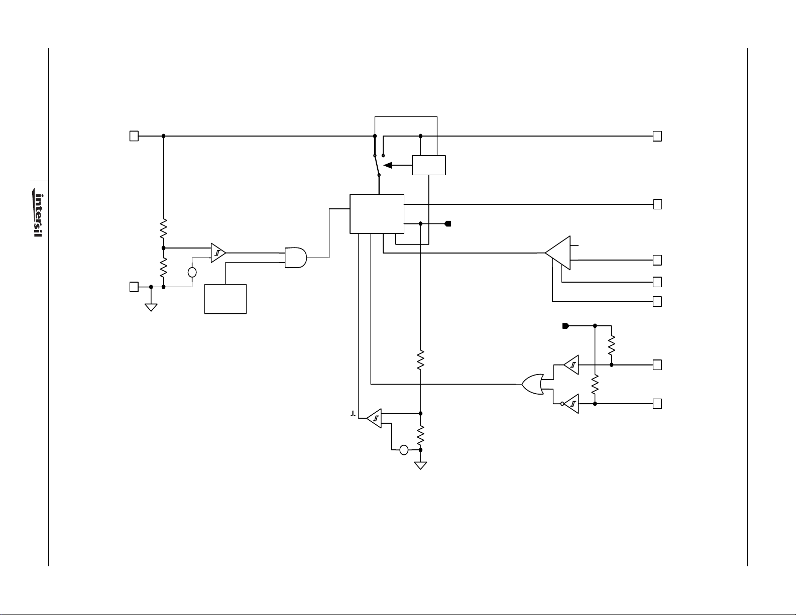
Functional Block Diagram
VPWR
105V MAX
2
VSW
POR
REGULATOR
INT . BIAS
-
+
GND
START/STOP
UV COMPARATOR
+
BG
-
+
-
TMON
+150ºC TRIP
+95ºC CLEAR
VPWR OK
TEMP OK
ENABLE
INP UT
SELECTOR
INT-ENABLE
INT. BIAS
INT . BIA S
1.5V REF
+
_
0V TO 40V
1.5V TO 20V
@ 100mA
AUXIN
VSW
VSW_FB
COMPA
COMPB
ENABLE
ENABLE_N
ISL6719
-
+
BG
October 1, 2007
FN6555.1
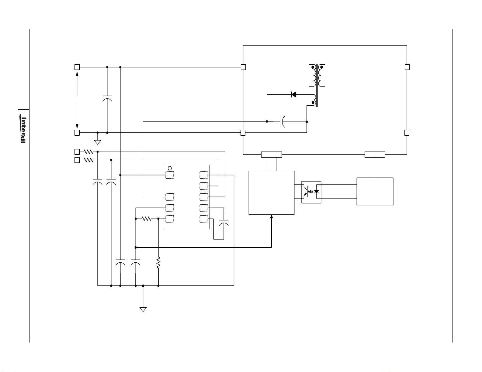
Typical Application
CONVERTER POWER STAGE
VIN
+
3
17V TO 100V
VIN-
ENABLE
DISABLE
1
VPWR
ENABLE_N
2
AUXIN
3
4
VSW_FB
R1
ISL6719
GND
ENABLE
COMPBVSW
COMPA
9
8
7
6
5
C3
220pF
PWM
FEEDBACK
AMP L IF IER
+VOUT
RETURN
ISL6719
C1
October 1, 2007
FN6555.1
C2
1.0μF
R2

ISL6719
Absolute Maximum Ratings Thermal Information
Supply Voltage, VPWR . . . . . . . . . . . . . . . . . .GND - 0.3V to +105V
AUXIN, VSW_FB. . . . . . . . . . . . . . . . . . . . . . . .GND - 0.3V to +40V
COMPB . . . . . . . . . . . . . . . . . . . . . . . . . . . . . . .GND - 0.3V to +30V
VSW. . . . . . . . . . . . . . . . . . . . . . . . . . . . . . . . . . GND - 0.3V to +25V
All Others. . . . . . . . . . . . . . . . . . . . . . . . . . . . . GND - 0.3V to +6.0V
Operating Conditions
Temperature Range
ISL6719AARZ . . . . . . . . . . . . . . . . . . . . . . . . . . .-40°C to +105°C
Supply Voltage Range (Typical). . . . . . . . . . . . . . 18VDC to 80VDC
CAUTION: Do not operate at or near the maximum ratings listed for extended periods of time. Exposure to such conditions may adversely impact product reliability and
result in failures not covered by warranty.
NOTES:
is measured with the component mounted on a high effective thermal conductivity test board in free air. See Tech Brief TB379 for details.
1. θ
JA
2. For θ
3. All voltages are with respect to GND.
, the “case temp” location is the center of the exposed metal pad on the package underside.
JC
Electrical Specifications Recommended operating conditions unless otherwise noted. Refer to “Functional Block Diagram” on page 2
and “Typical Application” on page 3. 17V < VPWR < 100V, C
T
= -40°C to +105°C (Note 4), Typical values are at TA = +25°C.
A
PARAMETER TEST CONDITIONS MIN TYP MAX UNITS
SUPPLY VOLTAGE (VPWR)
Supply Voltage 100 V
Start-Up Current (I
Operating Current (I
UVLO START Threshold VSW Disabled 13.0 16.5 V
UVLO STOP Threshold VSW Disabled 12.0 15.0 V
Hysteresis UVLO START - UVLO STOP 0.8 1.2 1.7 V
AUXILIARY VOLTAGE (AUXIN)
Maximum Bias VPWR = 17V, 100V 40 V
OUTPUT VOLTAGE (VSW)
Load Capacitance Range Note 5 0.47 1.0 1.5 µF
Overall Accuracy VPWR = 18V, 100V, VSW = 5V, 10V, 12V
Setpoint Range VPWR = 100V, AUXIN = 30V 1.55 20 V
Reference VSW_FB = VSW 1.45 1.50 1.55 V
Source Voltage Headroom (AUXIN - VSW) VPWR = 17V, VSW = 10V, I
Source Voltage Headroom (VPWR - VSW) VSW = 20V, AUXIN = 0V
Minimum Required Load -3 mA
) VPWR = 12V 250 450 µA
VPWR
) VSW Enabled, VPWR = 100V , VSW = 10V, 20V ,
VPWR
I
VPWR
- I
VSW
VSW Disabled, VPWR = 100V, 1.1 2.0 mA
AUXIN Biased at 40V, VSW Enabled,
VPWR = 100V, VSW = 10V, 20V,
= -100mA
I
VSW
AUXIN = 15V, I
I
= -100mA 1.8 3.0 V
VSW
I
= -50mA 1.4 2.0 V
VSW
I
= -100mA 6.2 V
VSW
I
= -50mA 5.2 V
VSW
= -3mA to -100mA
VSW
Thermal Resistance (Typical, Notes 1, 2) θ
(°C/W) θJC (°C/W)
JA
9 Ld DFN . . . . . . . . . . . . . . . . . . . . . . . 54 2.8
Maximum Junction Temperature . . . . . . . . . . . . . . .-55°C to +150°C
Maximum Storage Temperature Range. . . . . . . . . .-65°C to +150°C
Pb-free reflow profile . . . . . . . . . . . . . . . . . . . . . . . . . .see link below
http://www.intersil.com/pbfree/Pb-FreeReflow.asp
VSW
= 1μF, I
= -3mA, VSW Enabled,
VSW
1.1 2.0 mA
1.1 2.0 mA
-5 +5 %
= 0.95*I
AUXIN
VSW
4
FN6555.1
October 1, 2007

ISL6719
Electrical Specifications Recommended operating conditions unless otherwise noted. Refer to “Functional Block Diagram” on page 2
and “Typical Application” on page 3. 17V < VPWR < 100V, C
T
= -40°C to +105°C (Note 4), Typical values are at TA = +25°C. (Continued)
A
PARAMETER TEST CONDITIONS MIN TYP MAX UNITS
Maximum VOUT, Faulted VSW_FB VSW_FB = 0V, VPWR = 100V, AUXIN = 40V 22 25 V
Long Term Stability T
= +125°C, 1000 hours (Note 5),
A
VPWR = 48V, VSW = 10V, I
AUXIN = 15V
VSW
= -10mA,
Operational Current (source) VPWR = 48V, AUXIN = 17V, VSW= 15V -100 mA
Current Limit VPWR = 48V, AUXIN = 15V, VSW= 10V -100 -230 -400 mA
VSW_FB Bias Current VPWR = 100V, AUXIN = 40V, VSW = 10V,
VSW_FB = 1.5V
COMPA, COMPB Recommended
Note 5 170 220 270 pF
Capacitance
COMPA Voltage 0.7 V
COMPB Voltage VSW + 5.0 V
ENABLE, ENABLE_N
High Level Input Voltage (VIH) VPWR = 48V, AUXIN = 0V 2.5 3.0 3.6 V
Low Level Input Voltage (VIL) VPWR = 48V, AUXIN = 0V 1.6 2.0 2.5 V
Hysteresis VPWR = 48V, AUXIN = 0V 0.7 1.0 1.3 V
Pull-Up Resistance V
Turn-On Delay T
Turn-Off Delay T
ENABLE =VN_ENABL
VSW,10%
I
VSW
VSW,10%
I
VSW
- T
ENABLE, TVSW,10%
= -3mA
- T
ENABLE, TVSW,10%
= -50mA
=0V - 100 - kΩ
- T
ENABLE_N,
- T
ENABLE_N,
THERMAL PROTECTION
Thermal Shutdown 150 °C
Thermal Shutdown Clear 95 °C
Hysteresis 55 °C
NOTE:
4. Specifications at -40°C and +105°C are guaranteed by +25°C test with margin limits.
5. Limits established by characterization and are not production tested.
VSW
= 1μF, I
= -3mA, VSW Enabled,
VSW
0.3 %
-0.5 1.5 µA
25 µs
40 µs
Typical Performance Curves
5.5
5.0
4.5
4.0
VPWR - VSW (V)
3.5
3.0
0 20 40 60 80 100
VSW CURRENT (mA)
FIGURE 1. VPWR - VSW vs I
@ AUXIN = 0V, +25°C FIGURE 2. AUXIN - VSW vs I
VSW
5
2.5
2.0
1.5
AUXIN - VSW (V)
1.0
0 20 40 60 80 100
VSW CURRENT (mA)
@ VPWR = 17V, +25°C
VSW
FN6555.1
October 1, 2007

Typical Performance Curves (Continued)
ISL6719
1.002
VSW = 1.5V, AUXIN = 15V
1.001
VSW = 5V, AUXIN = 15V
1.000
0.999
VSW = 12V, AUXIN = 15V
0.998
NORMALIZED REGULATION
0.997
FIGURE 3. VSW REGULATION vs TEMPERA TURE @
VSW = 15V, AUXIN = 30V
-40 -25 -10 5 20 35 50 65 80 95 1 10
TEMPERATURE (°C)
VPWR = 100V, I
VSW
VSW = 20V, AUXIN = 30V
= 3mA
Pin Descriptions
VPWR
VPWR is the power connection for the IC. UVLO
enables/disables the output and places the device into a
standby mode even if AUXIN is externally biased.
To optimize noise immunity, bypass VPWR to GND with a
ceramic capacitor as close to the VPWR and GND pins as
possible.
AUXIN
This is the input for an external bias source typically
provided by an auxiliary transformer winding. This input is
not required and may be grounded or left open. Maximum
input bias is 40V.
ENABLE
The positive logic on/off control input. A logic high enables
VSW. Asserting this signal low turns off VSW. ENABLE and
ENABLE_N are logically ORed. Either signal can enable
VSW, but both must be false to disable VSW.
ENABLE_N
The negative logic on/off control input. A logic low enables
VSW. Asserting this signal high turns off VSW . ENABLE and
ENABLE_N are logically ORed. Either signal can enable
VSW, but both must be false to disable VSW.
GND
Signal and power ground connections for this device.
VSW
This is the switched regulated low voltage output supply that
is derived from VPWR or AUXIN. Its output is adjustable
from 1.5V to 20V using an appropriate divider from VSW to
VSW_FB. Protection circuitry prevents the output from
exceeding 25V in the event of a fault on VSW_FB (short high
1.0010
1.0005
1.0000
0.9995
NORMALIZED OUTPUT VOLTAGE
0.9990
0 10 20 30 40 50 60 70 80 90 100
FIGURE 4. VSW REGULATION vs LOAD @ VPWR = 18V,
AUXIN = 15V, +25°C
VSW = 5V
VSW = 10V
VSW = 12V
LOAD (mA)
or low). The minimum output current capability is 100mA.
VSW requires a minimum load of 3mA.
VSW_FB
The feedback pin for VSW. A divider from VSW to ground
sets feedback for VSW and determines the output voltage.
COMPA, COMPB
A compensating capacitor is placed between COMPA and
COMPB to stabilize the control loop. The values may vary
depending on the output load and capacitance applied
between VSW and GND, but for all applications having a
1.0µF load capacitor, a 220pF compensation capacitor is
recommended. The voltage at COMPA is nominally 0.7V.
The voltage at COMPB is nominally VSW +5.0V.
Functional Description
Features
The control circuitry used in Telecom/Datacom DC/DC
converters typically requires an operating bias voltage
significantly lower than the source voltage available to the
converter. Many applications use a discrete linear regulator
from the input source to create the bias supply. Often an
auxiliary winding from the power transformer is used to
supplement or replace the linear supply once the converter
is operating. The auxiliary winding bias voltage may require
regulation as well to minimize the voltage variation inherent
in slave windings. When implemented discretely, this
circuitry occupies significant PWB area, a considerable
problem in today’s high density converters.
The ISL6719 linear regulator simplifies the start-up and
operating bias circuitry needed in Telecom and Datacom
DC/DC converters by integrating these functions, and more,
in a small 3mm x 3mm DFN package.
6
FN6555.1
October 1, 2007
AUXIN
AUXIN is the auxiliary input of the ISL6719, accepting bias
voltage whenever the input source voltage, VPWR, is above
its undervoltage lockout (UVLO) threshold. VSW selects
AUXIN as its source when it is capable supporting the load
on VSW. Otherwise VPWR is selected.
AUXIN can accept voltages up to 40V maximum. Voltages in
excess of 40V, including transients, will cause permanent
damage to the device. Care should be taken when
connecting external sources through very long traces or lead
wires. The lead inductance may cause unexpected
transients in excess of the device’s ratings. In such
circumstances it is recommended that a small resistor be
placed between AUXIN and the external source to dampen
the transient. A value of 10Ω to 100Ω is usually sufficient.
VSW
VSW is the switched output and may be turned on and off
using the ENABLE or ENABLE_N pins. VSW is adjustable
from 1.5V to 20V, but must always be at least 6.2V lower
than VPWR at rated load. Additionally, VSW must be at least
3.0V lower than AUXIN for it to function as the source for
VSW. As the differential voltage between AUXIN and VSW
drops below 3.0V, the input current will shift from AUXIN to
VPWR. The voltage headroom required is load dependent.
See Figures 1 and 2. VSW preferentially uses AUXIN as its
input source, but if AUXIN is unable to supply adequate
voltage, VPWR is selected as the alternate input source.
VSW is capable of delivering up to 100mA continuously,
depending on power dissipation and the thermal
environment in which the device is placed.
The output voltage is adjusted using the VSW_FB input.
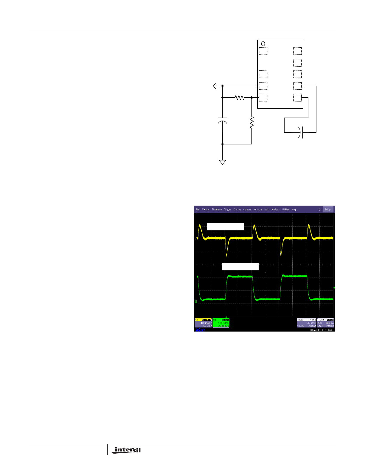
VSW is set with a resistor divider from VSW to ground with
the central node connected to VSW_FB. Refer to Figure 5.
R1R2+
VSW V
Referring to Equation 1, V
has a maximum value of 1.5µA. The error introduced by the
VSW_FB bias current can be minimized by making the
product of R
desired output voltage. For example, setting R
equal to 0.5% of VSW yields a value for R
VSW (kΩ).
REF
---------------------
x I
1
–= V
I
BIASR1
R
2
is nominally 1.5V and I
REF
small, relative to the magnitude of the
BIAS
x I
1
equal to 3.33 x
1
BIAS
(EQ. 1)
BIAS
ISL6719
1
VPWR
ENABLE_N
ENABLE
2
AUXIN
VSW
3
VSW
4
VSW_FB
R2
VSW
R1
C2
1.0μF
FIGURE 5. VSW ADJUSTMENT AND COMPENSATION
TRACE 1: VSW
TRACE 2: I
FIGURE 6. VSW TRANSIENT RESPONSE, 10mA TO 100mA
STEP, VPWR = 18V, AUXIN = 15V, VSW = 12V
GND
COMPB
COMPA
9
8
7
6
5
C3
220pF
VSW requires an external compensation capacitor to remain
stable across the output adjustment range, output
capacitance and loading. A value of 220pF between COMPA
and COMPB is recommended for all operating conditions
with a nominal load capacitance of 1.0µF (0.47µF to 1.5µF).
VSW requires a minimum load of 3mA.
7
Figure 6 depicts the transient response of VSW during a
10mA to 100mA step load when AUXIN is set to 15V and
VPWR is set to 18V.
VPWR
VPWR provides the source voltage for the IC and load until
AUXIN is back biased. VSW is disabled and the IC operates
in a standby (low power consumption) mode when UVLO is
active.
FN6555.1
October 1, 2007

ISL6719
If the application requires high currents or longer start-up
times than the thermal protection allows, the device
dissipation may be reduced by adding a resistor or resistors
in series between the input voltage and VPWR. The
dropping resistance must be selected such that VPWR
remains above the UVLO threshold of VPWR and at least
6.2V greater than VSW under maximum load and minimum
input voltage to maintain regulation.
VIN
1
VPWR
ENABL
2
ENABLE
AUXIN
3
VSW
COMPB
COMPA
4
VSW_FB
FIGURE 7. ADDING DROPPING RESISTORS TO VPWR
GND
E_N
9
8
7
6
5
ENABLE, ENABLE_N
ENABLE and ENABLE_N are complementary inputs used to
turn VSW on and off. Both polarities of the enable function
are provided to ease the interface to the application. VSW
may be enabled by either ENABLE or ENABLE_N, but both
inputs must be logically false to disable the output. Each
enable input has a nominal 100kΩ pull-up resistor to 5V .
TABLE 1. ENABLE, ENABLE_N TRUTH TABLE
INPUTS OUTPUT
ENABLE ENABLE_N VSW
00ON
01OFF
10ON
11ON
The inputs can accept voltages up to 6V maximum down to
0.3V below signal ground. Voltages beyond these limits,
including transients, may cause permanent damage to the
device. Care should be taken when connecting signal
sources through long connections or if significant ground
shift could occur between the source and the input. In such
circumstances, it is recommended that appropriate clamping
networks be used to prevent possible electrical overstress.
Over-Temperature Prot ection
The ISL6719 has an over-temperature shutdown
mechanism to protect the devic e from excessive dissipation.
VSW shutdown occurs approximately at +150°C. The
hysteresis is large so that the IC has sufficient time to
operate at start-up loading levels without re-triggering the
over-temperature protection.
8
FN6555.1
October 1, 2007

Dual Flat No-Lead Plastic Package (DFN)
ISL6719
(DAT UM B )
5
INDEX
AREA
(DATUM A)
5
INDEX
AREA
SEATING
PLANE
NX L
7
A
C
SIDE VIEW
12
N
BOTTOM VIEW
D
TOP
VIEW
D2
N-1
e
(Nd-1)Xe
REF .
D2/2
2X
A3
E2/2
NX b
4
76
0.10
E
A
NX k
E2
2X
L9.3x3
ABC0.15
0.15
CB
C
0.10
//
C
0.08
M
BAC
9 LEAD DUAL FLAT NO-LEAD PLASTIC PACKAGE
MILLIMETERS
SYMBOL
NOTESMIN NOMINAL MAX
A 0.80 0.90 1.00 A1 - - 0.05 A3 0.20 REF -
b 0.20 0.25 0.30 4, 7
D 3.00 BSC D2 1.85 2.00 2.10 6, 7
E 3.00 BSC E2 0.80 0.95 1.05 6, 7
e 0.50 BSC -
k0.60 - - -
L 0.25 0.35 0.45 7
N92
Rev. 0 3/06
NOTES:
1. Dimensioning and tolerancing conform to ASME Y14.5-1994.
2. N is the number of terminals.
3. All dimensions are in millimeters. Angles are in degrees.
4. Dimension b applies to the metallized terminal and is measured
between 0.15mm and 0.30mm from the terminal tip.
5. The configuration of the pin #1 identifier is optional, but must be
located within the zone indicated. The pin #1 identi fier may be
either a mold or mark feature.
6. Dimensions D2 and E2 are for the exposed pads which provide
improved electrical and thermal performance.
7. Nominal dimensions are provided to assist with PCB Land
Pattern Design efforts, see Intersil Technical Brief TB389.
8. COMPLIANT TO JEDEC MO-229-WEED-3 except for
dimensions E2 & D2.
C
L
NX (b)
4
SECTION "C-C"
(A1)
8
e
CC
FOR ODD TERMINAL/SIDE
TERMINAL TIP
L
All Intersil U.S. products are manufactured, assembled and tested utilizing ISO9000 quality systems.
Intersil Corporation’s quality certifications can be viewed at www.intersil.com/design/quality
Intersil products are sold by description only. Intersil Corporation reserves the right to make changes in circuit design, software and/or specifications at any time without
notice. Accordingly, the reader is cautioned to verify that data sheets are current before placing orders. Information furnished by Intersil is believed to be accurate and
reliable. However, no responsibility is assumed by Intersil or its subsidiaries for its use; nor for any infringements of patents or other rights of third parties which may result
from its use. No license is granted by implicat ion or oth erwise u nde r any p a tent or p at ent r ights of Intersil or its subsidiaries.
For information regarding Intersil Corporation and its products, see www.intersil.com
9
FN6555.1
October 1, 2007
 Loading...