®
ISL6622B
Data Sheet March 19, 2009
VR11.1 Compatible Synchronous
Rectified Buck MOSFET Drivers
The ISL6622B is a high frequency MOSFET driver designed
to drive upper and lower power N-Channel MOSFETs in a
synchronous rectified buck converter topology . The advanced
PWM protocol of ISL6622B is specifically designed to work
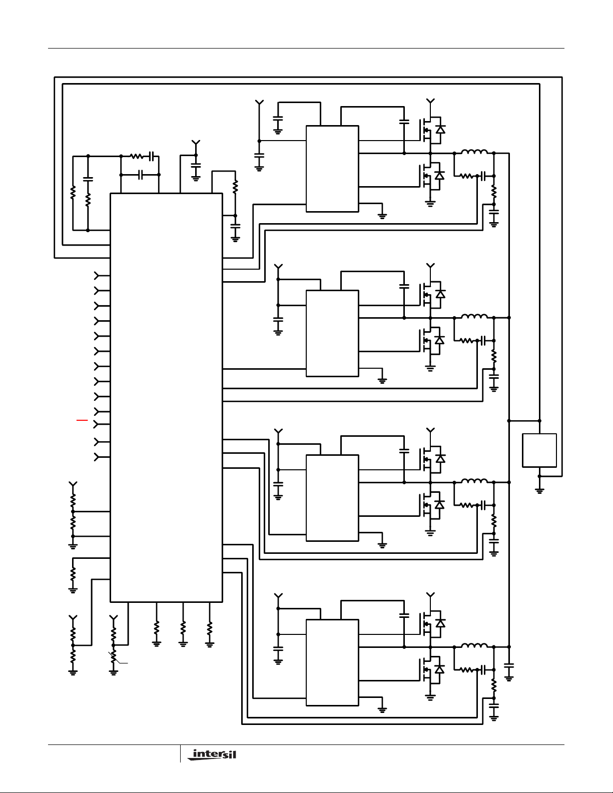
with Intersil VR11.1 controllers and combined with
N-Channel MOSFETs, form a complete core-volt age regulator
solution for ad va nc e d mi cr o pr oc e s sor s . When ISL6622B
detects a PSI
controller, it activates Diode Emulation (DE) operation;
otherwise, it operates in normal Continuous Conduction
Mode (CCM) PWM mode.
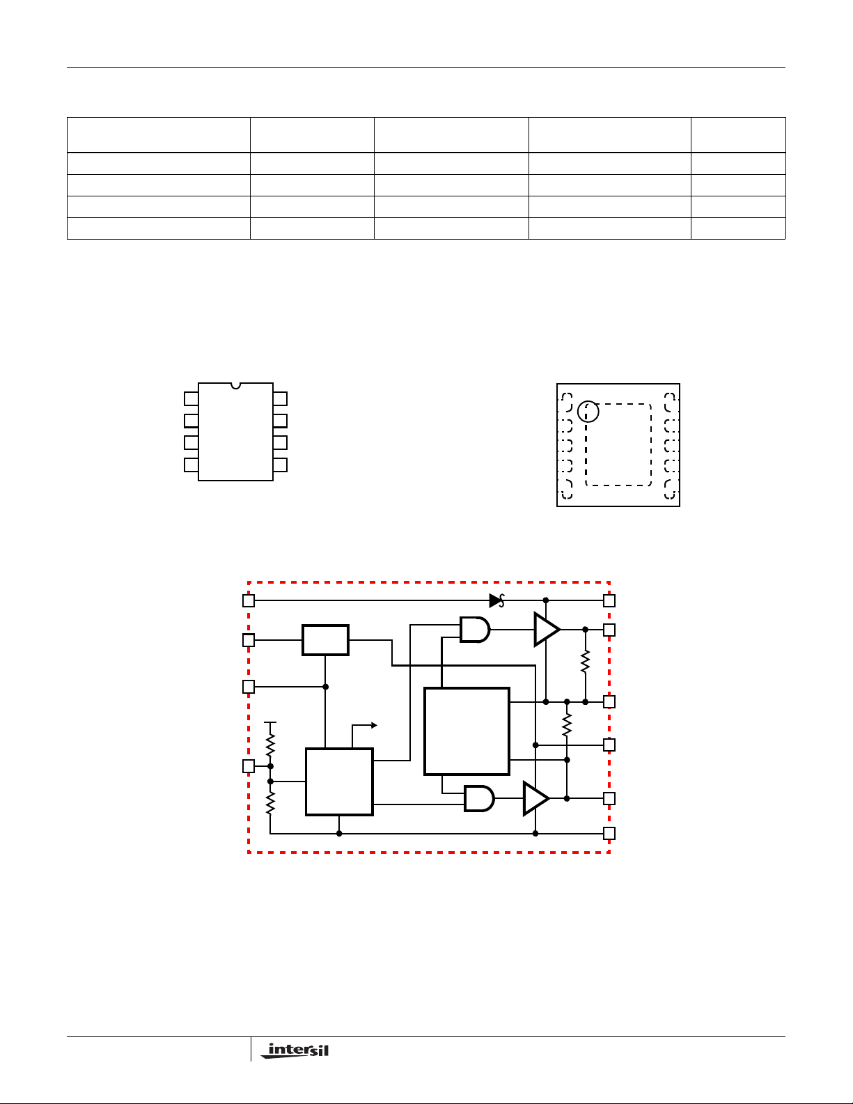
In the 8 Ld SOIC package, the ISL6622B drives the upper
gate to 12V while the lower drive voltage is fixed at 5.75V. The
10 Ld DFN part offers more flexibility: the upper gate can be
driven from 5V to 12V via the UVCC pin, while the lower gate
has a resistor-selectable drive voltage of 5.75V, 6.75V, and
7.75V (typically). This provides the flexibility necessary to
optimize applications involving trade-of fs betwe en gate
charge and conduction losses.
To further enhance light load efficiency, the ISL6622B
enables diode emulation operation during PSI
allows for Discontinuous Conduction Mode (DCM) operation
by detecting when the inductor current reaches zero and
subsequently turning off the low side MOSFET to prevent it
from sinking current.
An advanced adaptive shoot-through protection is integrated
to prevent both the upper and lower MOSFETs from
conducting simultaneously and to minimize dead time. The
ISL6622B has a 20k
gate-to-source resistor to prevent self turn-on due to high
input bus dV/dt. This driver also has an overvoltage
protection feature operational while VCC is below the POR
threshold: the PHASE node is connected to the gate of the
low side MOSFET (LGATE) via a 10k
output voltage of the converter close to the gate threshold of
the low side MOSFET, dependent on the current being
shunted, which provides some protection to the load should
the upper MOSFET(s) be shorted prior to start-up.
PWM protocol sent by an Intersil VR11.1
mode. This
Ω integrated high-side MOSFET
Ω resistor, limiting the
FN6602.1
Features
• Dual MOSFET Drives for Synchronous Rectified Bridge
• Advanced Adaptive Zero Shoot-Through Protection
• Integrated LDO with Selectable Lower Gate Drive Voltage
for Light Load Efficiency Optimization
• 36V Internal Bootstrap Diode
• Advanced PWM Protocol (Patent Pending) to Support PSI
Operation
• Diode Emulation for Enhanced Light Load Efficiency
• Bootstrap Capacitor Overcharging Prevention
• Supports High Switching Frequency
- 3A Sinking Current Capability
- Fast Rise/Fall Times and Low Propagation Delays
• Integrated UGATE-to-PHASE Resistor for Increased
Upper MOSFET Input Bus High dV/dt Immunity
• Pre-POR Overvoltage Protection at Start-Up and
Shutdown
• Dual Flat No-Lead (DFN) Package
- Near Chip-Scale Package Footprint; Improves PCB
Efficiency and Thinner in Profile
- Bottom Copper Pad for Enhanced Heat Sinking
• Pb-Free (RoHS Compliant)
Applications
• High Light-Load Efficiency Voltage Regulators
• Core Regulators for Advanced Microprocessors
• High Current DC/DC Converters
• High Frequency and High Efficiency VRM and VRD
Related Literature
• Technical Brief TB363 “Guidelines for Handling and
Processing Moisture Sensitive Surface Mount Devices
(SMDs)”
• Technical Brief TB417 “Designing Stable Compensation
Networks for Single Phase Voltage Mode Buck
Regulators” for Power Train Design, Layout Guidelines,
and Feedback Compensation Design
1
CAUTION: These devices are sensitive to electrostatic discharge; follow proper IC Handling Procedures.
1-888-INTERSIL or 1-888-468-3774
| Intersil (and design) is a registered trademark of Intersil Americas Inc.
Copyright Intersil Americas Inc. 2008, 2009. All Rights Reserved
All other trademarks mentioned are the property of their respective owners.

ISL6622B
Ordering Information
PART NUMBER
(Note)
ISL6622BCBZ* 6622B CBZ 0 to +70 8 Ld SOIC M8.15
ISL6622BCRZ* 622B 0 to +70 10 Ld 3x3 DF N L10.3x3
ISL6622BIBZ* 6622B IBZ -40
ISL6622BIRZ* 22BI -40
*Add “-T” suffix for tape and reel. Please refer to TB347 for details on reel specifications.
NOTE: These Intersil Pb-free plastic packaged products employ special Pb-free material sets, molding compounds/die attach materials, and 100%
matte tin plate plus anneal (e3 termination finish, which is RoHS compliant and compatible with both SnPb and Pb-free soldering operations). Intersil
Pb-free products are MSL classified at Pb-free peak reflow temperatures that meet or exceed the Pb-free requirements of IPC/JEDEC J STD-020.
PART
MARKING
TEMP. RANGE
(°C)
to +85 8 Ld SOIC M8.15
to +85 10 Ld 3x 3 D FN L10.3x3
PACKAGE
(Pb-free)
PKG.
DWG. #
Pinouts
UGATE
BOOT
PWM
GND
Block Diagrams
ISL6622B
(8 LD SOIC)
TOP VIEW
1
2
3
4
UVCC
GD_SEL
VCC
PWM
ISL6622B
(10 LD 3x3 DFN)
TOP VIEW
8
PHASE
7
6
5
VCC
LVCC
LGATE
UGATE
1
BOOT
2
GD_SEL
3
4
PWM
5
GND LGATE
PAD
10
9
8
7
6
PHASE
VCC
UVCC
LVCC
ISL6622B
BOOT
UGATE
PHASE
LVCC
LGATE
+5V
11.2k
9.6k
LDO
POR/
CONTROL
LOGIC
LVCC
SHOOT-
THROUGH
PROTECTION
20k
10k
GND
LVCC = 5.75V (TYPICALL Y) at 50mA for SOIC
2
UVCC = VCC for SOIC
March 19, 2009

Typical Application Circuit
ISL6622B
VTT
VR_RDY
VID7
VID6
VID5
VID4
VID3
VID2
VID1
VID0
PSI
VR_FAN
VR_HOT
VIN
+5V
VDIFF
VSEN
RGND
EN_VTT
EN_PWR
GND
IMON
TCOMP
TM
+5V
+5V
COMPFB
PWM1
ISEN1-
ISEN1+
ISL6334
ISL6334
PWM2
ISEN2-
ISEN2+
PWM3
ISEN3-
ISEN3+
PWM4
ISEN4-
ISEN4+
OFS FS SS
DACVCC
REF
+12V
+12V
+12V
+12V
LVCC
VCC
PWM
PVCC
VCC
PWM
PVCC
VCC
PWM
PVCC
ISL6622B
DRIVER
ISL6612
DRIVER
ISL6612
DRIVER
BOOT
UGATE
PHASE
LGATE
GND
BOOT
UGATE
PHASE
LGATE
GND
BOOT
UGATE
PHASE
LGATE
GND
BOOT
VIN
VIN
VIN
µP
LOAD
VIN
NTC
VCC
ISL6612
DRIVER
PWM
3
UGATE
PHASE
LGATE
GND
March 19, 2009

ISL6622B
Absolute Maximum Ratings Thermal Information
Supply Voltage (VCC, UVCC) . . . . . . . . . . . . . . . . . . . . . . . . . . .15V
BOOT Voltage (V
Input Voltage (V
UGATE. . . . . . . . . . . . . . . . . . . V
V
LGATE. . . . . . . . . . . . . . . . . . GND - 0.3V
BOOT-GND
PWM
- 3.5V (<100ns Pulse Width, 2µJ) to V
PHASE
GND - 5V (<100ns Pulse Width, 2µJ) to V
PHASE. . . . . . . . . . . . . . . . . . . . . . . . . . . . GND - 0.3V
GND - 8V (<400ns, 20µJ) to 30V (<200ns, V
CAUTION: Do not operate at or near the maximum ratings listed for extended periods of time. Exposure to such conditions may adversely impact product reliability and
result in failures not covered by warranty.
). . . . . . . . . . . . . . . . . . . . . . . . . . . .36V
) . . . . . . . . . . . . . . . . . . . . . .GND - 0.3V to 7V
PHASE
- 0.3VDC to V
to V
DC
LVCCLVCC
LVCCLVCC
BOOT-GND
BOOT
BOOT
to 15V
DC
+ 0.3V
+ 0.3V
+ 0.3V
+ 0.3V
DC
<36V)
NOTES:
is measured with the component mounted on a high effective thermal conductivity test board in free air. See Tech Brief TB379 for details.
1. θ
JA
is measured in free air with the component mounted on a high effective thermal conductivity test board with “direct attach” features. See
2. θ
JA
Tech Brief TB379.
3. For θ
, the “case temp” location is the center of the exposed metal pad on the package underside.
JC
4. Limits should be considered typical and are not production tested.
Z
Electrical Specifications Recommended Operating Conditions. Parameters with MIN and/or MAX limits are 100% tested at +25°C,
unless otherwise specified. Temperature limits established by characterization and are not production
tested.
PARAMETER SYMBOL TEST CONDITIONS MIN TYP MAX UNITS
VCC SUPPLY CURRENT
No Load Switching Supply Current I
Standby Supply Current I
VCC
I
VCC
I
UVCC
VCC
I
VCC
I
UVCC
ISL6622BCBZ and ISL6622BIBZ,
f
PWM
ISL6622BCRZ and ISL6622BIRZ,
f
PWM
ISL6622BCBZ and ISL6622BIBZ, PWM
Transition from 0V to 2.5V
ISL6622BCRZ and ISL6622BIRZ, PWM
Transition from 0V to 2.5V
POWER-ON RESET
VCC Rising Threshold 6.25 6.45 6.70 V
VCC Falling Threshold 4.8 5.0 5.25 V
LVCC Rising Threshold (Note 4) -4.4- V
LVCC Falling Threshold (Note 4) -3.4- V
PWM INPUT (See “TIMING DIAGRAM” on page 6)
Input Current I
PWM
V
PWM
V
PWM
PWM Rising Threshold VCC = 12V - 3.4 - V
PWM Falling Threshold VCC = 12V - 1.6 - V
Tristate Lower Gate Falling Threshold VCC = 12V - 1.60 - V
Tristate Lower Gate Rising Threshold VCC = 12V - 1.1 - V
Tristate Upper Gate Rising Threshold VCC = 12V - 3.2 - V
Tristate Upper Gate Falling Threshold VCC = 12V - 2.8 - V
Thermal Resistance θ
(°C/W) θJC (°C/W)
JA
SOIC Package (Note 1) . . . . . . . . . . . . 100 N/A
DFN Package (Notes 2, 3). . . . . . . . . . 48 7
Maximum Junction Temperature (Plastic Package) . . . . . . .+150°C
Maximum Storage Temperature Range. . . . . . . . . .-65°C to +150°C
Pb-Free Reflow Profile. . . . . . . . . . . . . . . . . . . . . . . . .see link below
http://www.intersil.com/pbfree/Pb-FreeReflow.asp
Recommended Operating Conditions
Ambient Temperature Range
ISL6622BIBZ, ISL6622BIRZ . . . . . . . . . . . . . . . . .-40°C to +85°C
ISL6622BCBZ, ISL6622BCRZ. . . . . . . . . . . . . . . . . 0°C to +70°C
Maximum Operating Junction Temperature. . . . . . . . . . . . . +125°C
Supply Voltage, VCC. . . . . . . . . . . . . . . . . . . . . . . . . . 6.8V to 13.2V
Supply Voltage Range, UVCC. . . . . . . . . . . . . . . . . .4.75V to 13.2V
-8.6-mA
= 300kHz, V
= 300kHz, V
= 5V - 500 - µA
= 0V - -430 - µA
VCC
VCC
= 12V
= 12V
-6.6-mA
-2-mA
-5.1-mA
-5.0-mA
-0.07- mA
4
March 19, 2009
 Loading...