

Page 1
®
ISL6590
Data Sheet April 2003
Digital Multi-Phase PWM Controller for
Core-Voltage Regulation
Processors that operate above a GHz require fast, intelligent
power systems. The Intersil ISL6590 controller offers
intelligent digital, multi-phase control that provides high
bandwidth, optimal control frequency response, noise
immunity and active transient response control algorithms.
The design is fully scalable for controlling up to six phases,
each featuring the Intersil ISL6580 intelligent power stage.
The user can configure and monitor the power system via
the Asynchronous Serial Interface (ASI). The ISL6590
controller flexibility can be extended with the addition of an
external EEPROM for updating key circuit operating
parameters in the control loop and overall system design.
The digital architecture reduces the design time for
engineers with the use of our software. The software allows
the designer the freedom to choose output stage
components and still achieve optimized system
performance.
The ISL6590 digital controller communicates with the
ISL6580 integrated power stages via 100% digital signaling.
Serial communication allows for separation of the controller
and the power stage, providing placement and layout
freedom to the power stage. The digital controller
implements phase balancing to ensure even distribution of
phase currents. The ISL6590 controller configures the
ISL6580 power stage current limit, VID reference, nonoverlap period, Active Transient Response (ATR) trigger
levels and maximum temperature limit. The digital controller
also monitors the ISL6580 power stage peak currents, overtemperature fault, input under voltage, output over/under
voltage to ensure proper operation of the power supply.
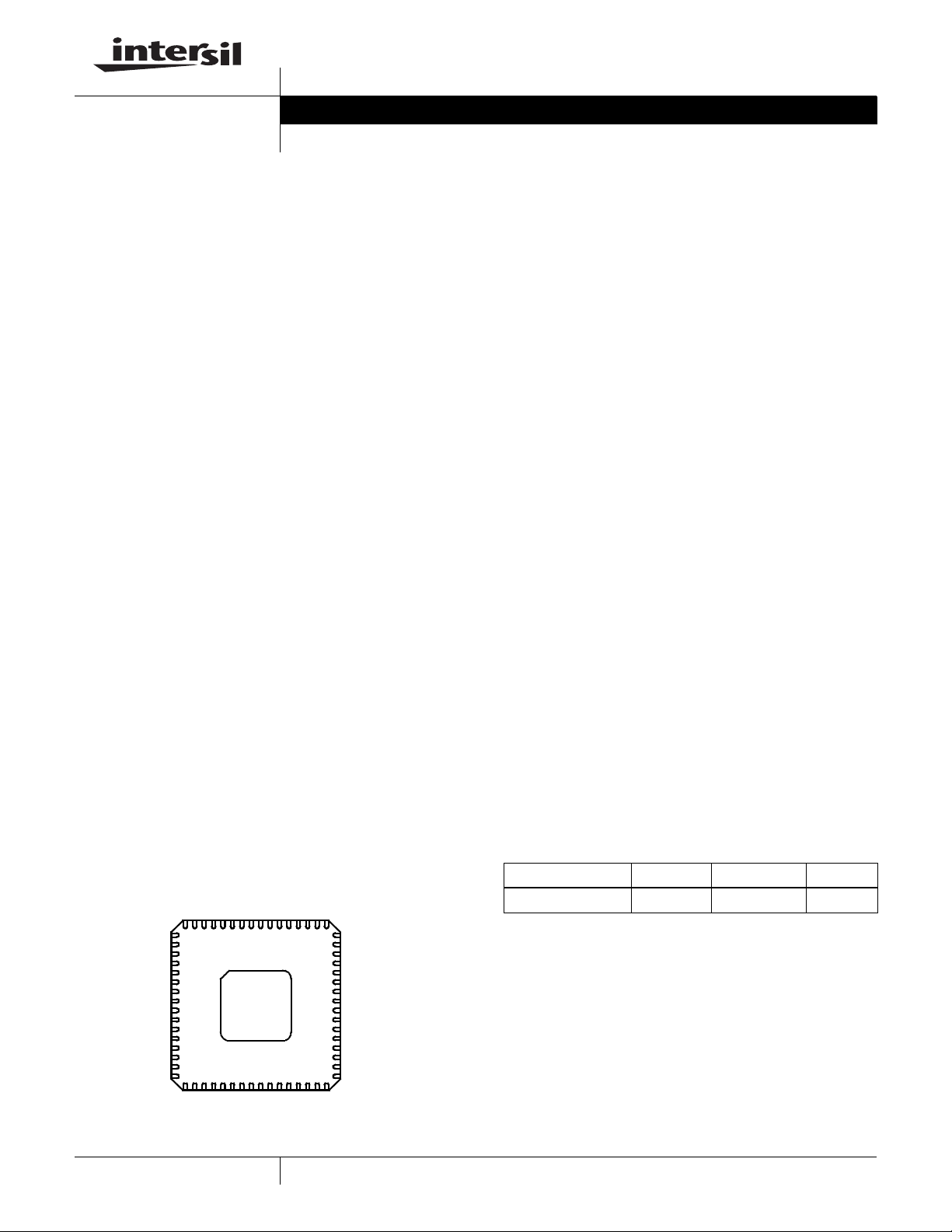
Pinout
ISL6590 (QFN)
TOP VIEW
FN9061
Features
• Open Architecture features software programmable
control loop compensation enabling optimal system
performance
- User accessible asynchronous serial interface
• Intel VR10
- 6-bit Dynamic VID™
- Output voltage regulation range of 0.8375V to 1.600Vdc
• 250kHz to 1MHz switching frequency
• 100% digital control and signaling
• Active Transient Response (ATR) control algorithms for
minimized voltage droop and overshoot
• Controls up to six ISL6580 intelligent power stages (20A
per phase, 120A total system current)
• Programmable Adaptive voltage positioning (AVP) load
line
• Configurable control loop parameters (with optional
external EEPROM)
• Programmable MOSFET dead time control
• High speed voltage and current control loops
• PWRGD and OUTEN
• Serial interface to ISL6580 power stages for system
monitoring and configuration
• 64 Ld 9x9 QFN package
• QFN Package Option
- QFN Compliant to JEDEC PUB95 MO-220 QFN - Quad
Flat No Leads - Product Outline
- QFN Near Chip Scale Package Footprint; Improves
PCB Efficiency, Thinner in Profile.
Ordering Information
OUTEN
VID [0]
VID [1]
VID [2]
VID [3]
VID [4]
VID [5]
VDD_CORE
PWRGD
VDD_IO
MCLK
MDO
MCS
NDRIVE1
PWM1
PART NUMBER TEMP. (oC) PACKAGE PKG. NO.
ISL6590DR 0 to 85 64 Ld 9x9 QFN L64.9x9-S
PLL_FILTER
PLL_ANALOG_VDD
PLL_ANALOG_VSS
PLL_DIGITAL_VSS
OSC_IN
OSC_OUT
ARX
ATX
VDD_IO
SCLK
SDATA
TEST4
TEST3
PLL_DIGITAL_VDD
VDD_CORE
64
01
MDI
16
IDIG1
IDIG2
VDD_CORE
NDRIVE3
IDIG3
PWM3
VDD_IO
NDRIVE4
NDRIVE2
PWM2
1
ATRH
49
TEST 2
48
ATRL
SOC
ERR
VDD_IO
SYS_CLK
VDD_IO
NC
NC
VDD_CORE
NC
NC
IDIG6
PWM6
NDRIVE6
33
TEST1
3217
IDIG4
IDIG5
PWM5
PWM4
NDRIVE5
EXT_RESETB
CCAUTION: These devices are sensitive to electrostatic discharge; follow proper IC Handling Procedures.
1-888-INTERSIL or 321-724-7143
All other trademarks mentioned are the property of their respective owners. Dynamic VID™ is a trademark of Intersil Americas Inc.
| Intersil (and design) is a registered trademark of Intersil Americas Inc.
Copyright © Intersil Americas Inc. 2003. All Rights Reserved
Page 2
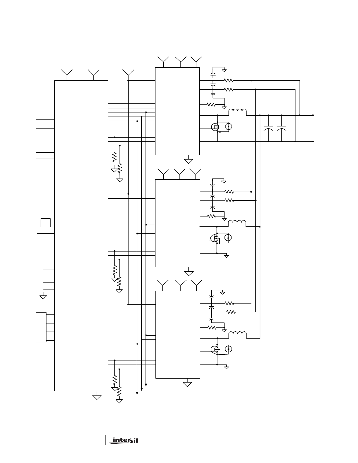
Typical Application Circuit
ISL6590
3.3 V
5-12 V 12 V
3.3 V
V DD_IO V DD_CORE
VID[0:5]
PWRGD
OUTEN
ARX
ATX
1.8 V
SCLK
SDATA
SYSCLK
PWM
NDRIV E
ISL6590
ATRH
ATRL
OSC_IN
OSC_OUT
ERR
SOC
IDIG
2.5 V
VDD VDRIVEVCC
VREF
ATRH
ATRL
ISL6580
ERR
SOC
SCLK
SDATA
CLK
PWM
IDIG
NDRIV E
3.3 V
VDD VDRIVEVCC
VREF
ATRH
ATRL
ISENSE
5-12 V
ISL6580
ERR
SOC
SCLK
SDATA
CLK
ISENS E
VSENP
VSENN
VSW
NGA TE
PGND
GND
12 V
VSENP
VSENN
VSW
NGA TE
REGULATION
CHANNEL
Vout
Vout
RTN
PWM
IDIG
NDRIV E
TEST1
TEST2
TEST3
TEST4
MDO
MDI
EEPROM
MCS
MCL K
PWM
IDIG
NDRIV E
GND
CONTROLLER
INTE RFACE BUS
PWM
IDIG
NDRIV E
5-12 V 12 V
3.3 V
VDD VD RI VEVCC
VREF
ATRH
ATRL
ISL6580
ERR
SOC
SCLK
SDATA
CLK
PWM
IDIG
NDRIV E
PGND
GND
VSENP
VSENN
ISENS E
VSW
NGA TE
PGND
GND
ATR CHANNEL
UV/OV CHANNEL
2
Page 3
ISL6590
Absolute Maximum Ratings
Supply Voltage
(VDD_IO) . . . . . . . . . . . . . . . . . . . . . . . . . . . . . . . . . . . . . . +3.63V
(VDD_Core) . . . . . . . . . . . . . . . . . . . . . . . . . . . . . . . . . . . . +1.98V
ESD Classification . . . . . . . . . . . . . . . . . . . . . . . . . . . . . . . . . . 1.5kV
Recommended Operating Conditions
Supply Voltage
(VDD_IO) . . . . . . . . . . . . . . . . . . . . . . . . . . . . . . . . . . . +3.3V ±5%
(VDD_Core) . . . . . . . . . . . . . . . . . . . . . . . . . . . . . . . . . +1.8V ±5%
(Analog PLL) . . . . . . . . . . . . . . . . . . . . . . . . . . . . . . . . +1.8V ±5%
(Digital PLL) . . . . . . . . . . . . . . . . . . . . . . . . . . . . . . . . . +1.8V ±5%
Ambient Temperature . . . . . . . . . . . . . . . . . . . . . . . . . .0
CAUTION: Stress above those listed in “Absolute Maximum Ratings” may cause permanent damage to the device. This is a stress only rating and operation of the
device at these or any other conditions above those indicated in the operational section of this specification is not implied.
o
C to 85oC
Thermal Information
Thermal Resistance (oC/W)
. . . . . . . . . . . . . . . . . . . . . . . . . . . . 3
θ
JC
θ
JA-0 LFPM AIR
θ
JA-100 LFPM AIR
θ
JA-200 LFPM AIR
θ
JA-400 LFPM AIR
θ
. . . . . . . . . . . . . . . . . . . . . . . . . . . . 8
JB
Maximum Storage Temperature Range . . . . . . . . . -65
Maximum Lead Temperature (Soldering 10s). . . . . . . . . . . . .300
Maximum Junction Temperature. . . . . . . . . . . . . . . . . . . . . . .125
Maximum Storage Temperature Range . . . . . . . . . -65
Maximum Lead Temperature (Soldering 10s). . . . . . . . . . . . .300
. . . . . . . . . . . . . . . . . . . 29.0
. . . . . . . . . . . . . . . . . 26.6
. . . . . . . . . . . . . . . . . 25.0
. . . . . . . . . . . . . . . . . 23.2
o
C to 150oC
o
C to 150oC
o
o
o
NOTE:
is measured with the component mounted on a “High Effective” Thermal Conductivity Board with “Direct Attach” features. (See Tech Brief
1. θ
JA
TB379 for details.)
Electrical Specifications Operating Conditions: V
DDIO
= 3.3V, V
DDCORE
= 1.8V, TA = 25oC, Unless Otherwise Specified
PARAMETER TEST CONDITIONS MIN TYP MAX UNITS
INPUTS
Outen, VID[0:5], V
Outen, VID[0:-5], V
IH
IL
MDI, IDIG[1-6], ATRL, ATRH, SOC,
ERR V
IH
MDI, IDIG[1-6], ATRL, ATRH, SOC,
ERR V
IL
EXT_RESETB, V
EXT_RESETB, V
ARX, V
IH
ARX, V
IL
OSC_IN, V
OSC_IN, V
IH
IL
IH
IL
3.3V no internal pull-up/down resistors 0.8 - - V
3.3V no internal pull-up/down resistors - - 0.4 V
3.3V internal pull-down resistor 2.0 - - V
3.3V internal pull-down resistor - - 0.8 V
3.3V internal pull-up resistor 2.0 - - V
3.3V internal pull-up resistor - - 0.8 V
3.3V internal pull-up resistor 2.0 - - V
3.3V internal pull-up resistor - - 0.8 V
No internal pull-up/down resistors 2.0 - - V
No internal pull-up/down resistors - - 0.8 V
OUTPUTS
MCLK, MDO, MCS, NDRIVE[0:5],
PWM[0:5], ATX, V
OH
MCLK, MDO, MCS, NDRIVE[0:5],
PWM[0:5], ATX, V
SYS_CLK, V
SYS_CLK, V
SCLK, V
SCLK, V
OH
OL
SDATA, V
SDATA, V
SDATA, V
SDATA, V
PWRGD, V
PWRGD, V
OSC_OUT, V
OSC_OUT, V
OL
OH
OL
OH
OL
IH
IL
OH
OL
OH
OL
No internal pull-up/down resistors, 8mA drive 2.4 - - V
No internal pull-up/down resistors, 8mA drive - - 0.4 V
No internal pull-up/down resistors, 20mA drive 2.4 - - V
No internal pull-up/down resistors, 20mA drive - - 0.4 V
No internal pull-up/down resistors, 16mA drive 2.4 - - V
No internal pull-up/down resistors, 16mA drive - - 0.4 V
3.3V pull-up resistor, 16mA drive 2.4 - - V
3.3V pull-up resistor, 16mA drive - - 0.4 V
3.3V pull-up resistor 2.0 - - V
3.3V pull-up resistor - - 0.8 V
Open drain, 6mA drive 2.4 - - V
Open drain, 6mA drive - - 0.4 V
No internal pull-up/down resistors, 10mA drive 2.4 - - V
No internal pull-up/down resistors, 10mA drive - - 0.4 V
C
C
C
3
Page 4
ISL6590
Electrical Specifications Operating Conditions: V
DDIO
= 3.3V, V
DDCORE
= 1.8V, TA = 25oC, Unless Otherwise Specified (Continued)
PARAMETER TEST CONDITIONS MIN TYP MAX UNITS
POWER-ON RESET AND ENABLE
POR Threshold V
Rising 1.4 - - V
ddio
V
Falling - - 2.55 V
ddio
V
ddcore Rising
V
ddcore Falling
0.7 - - V
--1.4V
OUTEN Threshold OUTEN Rising -0.71- V
OUTEN Falling -0.64- V
OSCILLATOR
Adjustment Range 0.250 - 1 MHz
Max Duty Cycle 24 TBD - %
NOTE:
1. Reserved for note.
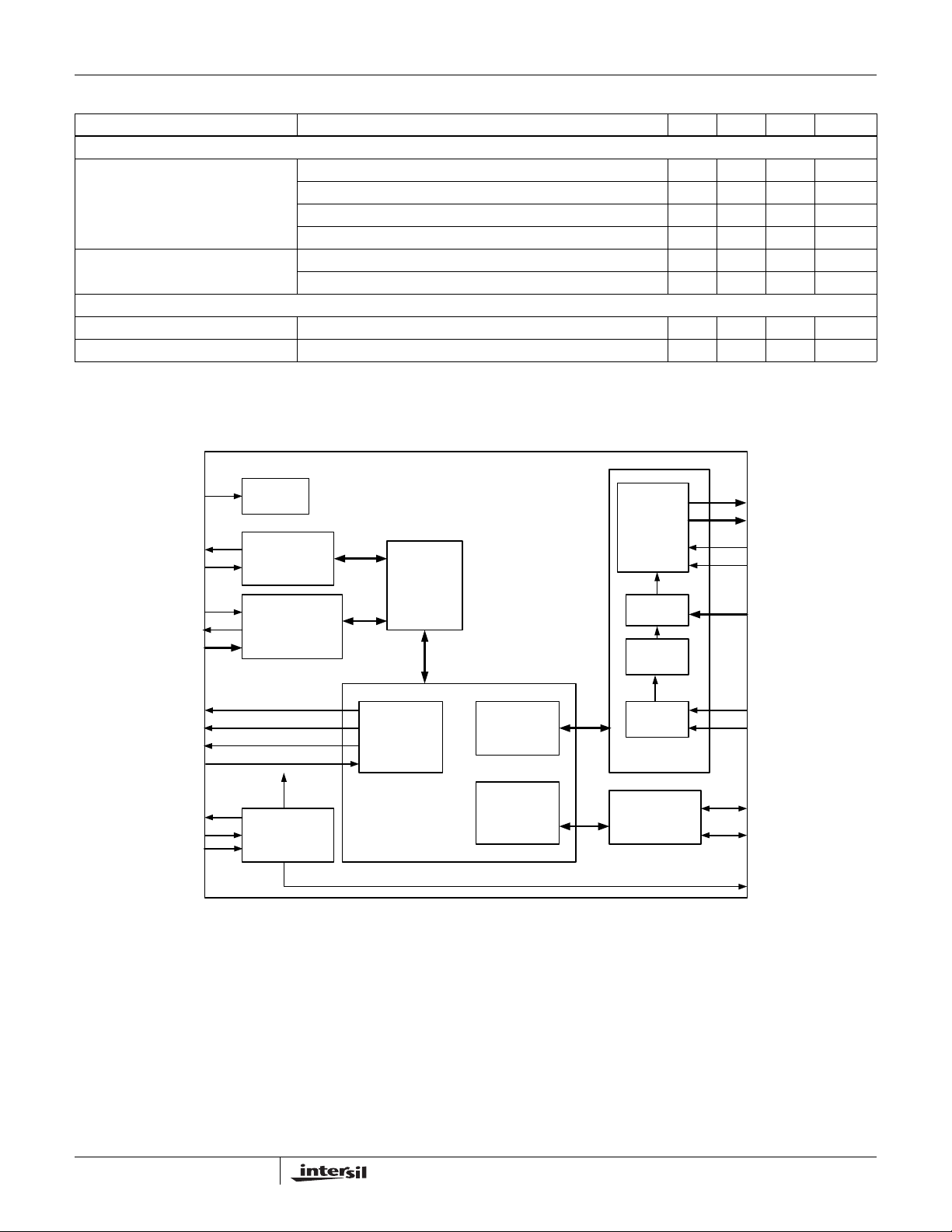
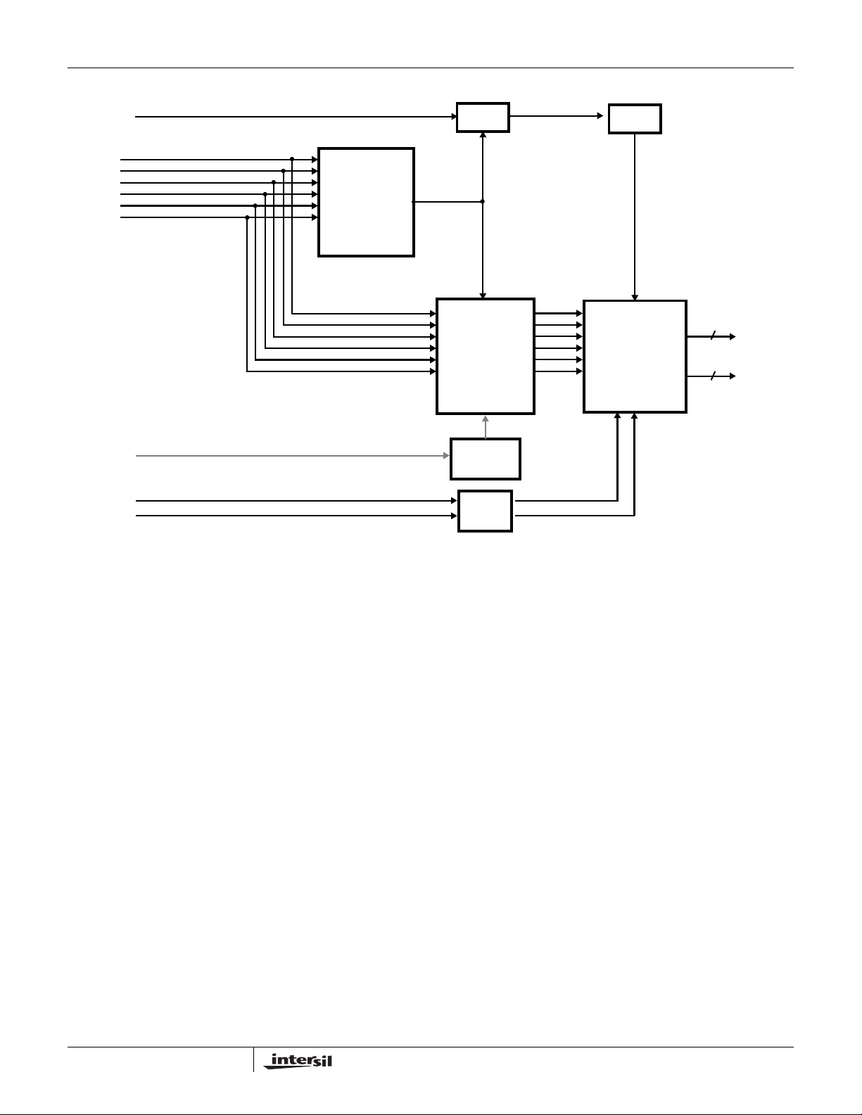
Block Diagram
Ext_Reset
ATX
ARX
OUTEN
PWRGD
VID[5:0]
POR
Asynchronous
Serial Interface
State
Control and
Fault
Moni tor
Memory Bus
MUX
Feedback
Control
PWM Driver
Current
Loop
Voltage
Loop
PWM [6:1]
NDRIVE [6: 1]
ATRH
ATRL
IDIG[6:1]
MDI
MCLK
MCS
MDO
OSC_OUT
OSC_IN
PLL_FILTER
Clock
Distribution
Non-Volatile
SPI EEPOM
Interface
State
Machine
Control/
Status
Registers
MHz Memory
Mapped
Registers
FIGURE 1. ISL6590 BLOCK DIAGRAM
AVP
Backside Serial
Bus
SOC
ERR
SCLK
SDATA
SYS_CLK
4
Page 5

ISL6590
Pin Descriptions
PIN NO. PIN NAME TYPE PIN DESCRIPTION
1 OUTEN Input Output enable high input signal used to command the regulator on and a low input signal turns
the regulator off.
2-7 VID[0:5] Input Voltage identification (6 bit). Programs Vout regulation voltage.
8, 21, 39, 57 VDD_CORE Power IC internal core supply voltage (1.8 VDC logic).
9 PWRGD Output Power Good high output signal to indicate the regulator output voltage is within the specified
10, 25, 42,
44, 54
11 MCLK Output
12 MDO Output
13 MDI Input
14 MCS Output
15, 18, 22,
26, 30, 34
16, 19, 23,
27, 31, 35
17, 20, 24,
28, 32, 36
29 EXT_Reset Input Voltage identification (6 bit). Programs Vout regulation voltage.
33, 48, 50,
51
37, 38, 40,
41
43 SYSCLK Input/Output System clock which runs at a 133.3MHz rate used to clock the ISL6580. This is generated by the
45 ERR Input Serial data transmitted at a 66MHz (or SYSCLK/2) rate. This 6 bit voltage error is feedback into
46 SOC Input Start of Conversion signal initiated by the ISL6580’s Voltage A/D to create the ERR signal.
47 ATRL Input Active Transient Response Low input signal from the ISL6580 indicating a voltage overshoot on
49 ATRH Input Active Transient Response High input signal from the ISL6580 indicating a voltage droop on the
52 SDATA Input/Output Controller serial interface for communication, monitoring, and configuration data between the
53 SCLK Output Serial digital bus clock supplied for the 16.67MHz clocking that accompanies SDATA via the
55 ATX Output Asynchronous Serial Interface Transmit
56 ARX Input Asynchronous Serial Interface Receive
58 OSC_OUT Output Only used if part is using a crystal to generate the system clock.
59 OSC_IN Input Requires a 33.33MHz oscillator or crystal which is used to generate system clock.
60 PLL_DIG_VSS
61 PLL_DIG_VDD Power
62 PLL_ANA_VSS Ground Analog Ground for the 4X clock multiplier PLL.
63 PLL_ANA_VDD Power 1.8V power supply for the 4X clock multiplier PLL (1.8 VDC logic).
64 PLL_Filter Analog Input Filter cap for PLL.
65 GND Ground Paddle IC Ground
VDD_IO Power IC I/O input supply voltage (3.3 VDC logic).
NDRIVE[1:6] Output Low side drive signal used to initiate the ISL6580 to turn on the LSFET.
PWM[1:6] Output PWM performs pulse width modulation which is used to turn on the ISL6580’s power devices.
IDIG[1:6]
TEST[1:4] Output Test pins for part evaluation
NC N/A These pins have not been bonded out.
PLL Bypass
Input Current A/D data serial 7-bit digital word (MSB first). The first bit is a start bit (Start = 1). The
Ground
Input
range. A low signal indicates the voltage is not within range.
EEPROM external memory clock, data is clocked out of the IC on the rising edge and data is
clocked into the ISL6580 IC on the falling edge. Compliant with SPI™ EEPROMs.
EEPROM external memory data output. Compliant with SPI EEPROMs
EEPROM external memory data input. Compliant with SPI EEPROMs.
EEPROM external memory chip select (Active low). Compliant with SPI EEPROMs.
remaining 6 bits represent the sampled peak current in the drain of the particular ISL6580
P-Channel HSFET. (IDIG word transmission is triggered by the falling edge of the PWM signal.)
IDIG is an input that is received at SYSCLK/2, normally 66.6MHz.
internal PLL circuit to create a 4x frequency multiply of the OSC_IN frequency.
the control loop and used to regulate the output voltage.
the converter output.
converter output.
ISL6580 and ISL6590 controller.
Backside serial bus.
Digital Ground
Test mode to bypass PLL input to core.
1.8V power supply for the 4X clock multiplier PLL clock tree driver
for the 4X clock multiplier PLL.
.
(1.8 VDC logic).
5
Page 6

ISL6590
General Description
The ISL6590 is a multiphase digital controller optimized for
microprocessor core voltage generation in the 0.8375Vdc -
1.600Vdc output range and high current loading up to 150A
with a 12Vdc input. It is intended to be used as a chipset with
multiple ISL6580 power stages. The current per stage is up
to 25A and the switching frequency can operate from
250kHz to 1MHz. The adaptability of having a digital
controller with a serial data bus to the power stages means
that the control algorithms can be adjusted with software
instead of having to make hardware or board changes. All of
the features of the ISL6590 are available in applications that
require 3-6 phases of PWM (Pulse-Width Modulation) core
voltage regulation. For more information on the power stage,
consult the ISL6580 data sheet.
Block Diagram Overview
The ISL6590 contains functionality to control up to 6 power
stages with PWM core voltage regulation. The blocks
described follow the block diagram shown in Figure 1. For
additional help it would be useful to reference the block
diagram of the ISL6580, which is located in the ISL6580 data
sheet.
Asynchronous Serial Interface (ASI) (ATX, ARX)
This 2-wire serial data host interface is designed to transfer
command information from the designers PC to the
controller, such as adjustments to register settings. The ASI
is used during the design process to configure and test your
power supply settings. It allows the designer to change loop
coefficients to achieve the best response for their system
design. This serial bus runs at 115K baud rate to interface
with a host computer during testing.
Backside Serial Bus (BSB) (SDATA, SCLK)
The backside serial bus is a 2-wire communication between
the ISL6590 controller and the ISL6580 power ICs used for
transfer of control and status information. This bus is critical
for proper operation of the system, any miscommunications
will cause a bus error between the controller and power
stages and shutdown the power supply. A bus error can be
caused by poor routing of those lines or by a failed ISL6580.
Feedback (PWM, NDRIVE, ATR, IDIG, SOC, ERR)
The feedback control block implements the loop
compensation, hysteretic control, and switch driver. Defaults
for the loop compensation coefficients are retained in the
memory block. If the default values need to be optimized,
they can be adjusted using the ASI.
The PWM generator that drives NDRIVE and PWM derives
its waveform from a current balancing circuit that balances
the current to each phase. The current balancing circuit
requires information about the amount of current each phase
is supporting. This information is obtained using the 6-bit
current ADC in each ISL6580.
Each of the ISL6580s contains a 6-bit voltage ADC that can
be used to measure the difference between the core voltage
at the output and a reference voltage that is set by the VID
information. Even though each ISL6580 has the voltage
ADC, only one of them is required to use it.
When a large change in current occurs at the output load, a
large voltage transient also occurs. The ATRH and ATRL
levels are designed to trigger a temporary mode in which the
PWM generator aligns all phases or removes all phases in
order to quickly raise or lower the output voltage.
Controller Memory
The internal volatile memory provides control and status
registers which are reset to default states on each power up.
These registers can be altered with commands from the ASI,
the State Control and Fault Monitors, or the Serial Interface
with the ISL6580 Power ICs.
EEPROM Interface (MCS, MCLK, MDI, MDO)
An external EEPROM (non-volatile memory) can be used to
write custom information to the volatile memory. The nonvolatile memory can be modified via the ASI. The EEPROM
contains configuration values for a given design. The
ISL6590 uses the standard Serial Peripheral Interface
(SPI™) serial protocol for this memory.
be at least a 2K byte memory. Larger memory can be used
without problems, however the ISL6590 will utilize only 2K
bytes.
The EEPROM must
Clock Distribution (OSC_IN, OSC_OUT)
The clock distribution block creates the internal system clock
from an external clock source such as a crystal oscillator. It
performs a 4x frequency multiplication of the external clock
frequency. The maximum clock input is 33.33MHz for an IC
sample rate of 133.3MHz. It generates the read/write clock
for the ASI. The system clock is provided to the ISL6580s via
the SYS_CLK pin.
State Control and Fault Monitoring (OUTEN,
VID[5:0], PWRGD)
Implements control of the power system state and processes
fault information from the ISL6580 Power IC. All fault
detection within the system is accomplished within each
individual ISL6580 and is communicated to the ISL6590 via
the Backside Serial Interface. ISL6590 detects the fault
through constant polling of the ISL6580 fault registers and
responds by tristating the outputs or shutting down the
system which then requires a power cycle and initiates a
softstart sequence.
Memory Bus Multiplexer
Controls the priority of data transfer to the volatile memory
(control registers) from both the ASI and the state control
and fault monitoring. The state control and fault monitoring is
given priority over the ASI.
6
Page 7
6-BIT OFFSET BINARY
V
ERR
(FROM ERR SIGNAL - ISL6580 VOLTAGE ADC)
1
2
3
4
5
6
6-BIT SERIAL
IDIG
IDIG
IDIG
IDIG
IDIG
IDIG
CURRENT
AVERAGING
ISL6590
I
AVG
AVP
AVP
0
PID
PID
OUT
PWM[6:1]
ISHARE
ATRH
ATRL
(FROM ISL6580 ATRH AND ATRL SIGNALS)
FIGURE 2. FEEDBACK CONTROL DIAGRAM
Block Diagram Details
Feedback Control
At a minimum, there must be three ISL6580s available to
implement the following modes.
1. Regulation Mode (Voltage ADC)
2. Voltage Transient Mode (ATR Window Comparator)
3. Over/Under Voltage Mode (O/U Voltage Comparator)
Additional phases 4-6 are in normal conversion mode.
Located in the Feedback Control section of the ISL6590 is
an interface to the feedback information collected and
delivered by the analog ISL6580 power stages. To
understand the functionality of the ISL6590 feedback
algorithms, key blocks of the ISL6580 must be understood,
such as the ADC converters and the window comparator.
6-bit Current ADC (ISL6580)
A current ADC (Analog-to-Digital Converter) located in each
ISL6580 measures, converts, and transmits that driver’s
current back to the ISL6590 serially via the IDIG[6:1] bus.
The start of conversion is initiated on the falling edge of the
PWM input signal at the ISL6580 and the conversion takes
about 8 SYSCLK cycles. The SYSCLK signal is provided by
the ISL6590 to the ISL6580 and is equal to 4x the crystal
CURRENT
BALANCING
I
ERR
CURRENT
SHARE
FLASH
LOGIC
ATRH
ATRL
PWM
GENERATOR
PARALLEL LINES
NDRIVE[6:1]
(TO ISL6580s)
oscillator rate. The 6-bit current ADC is a successive
approximation converter, requiring one clock per bit, for a
total of 6 clocks. Another clock cycle is for transferring data
to the serial register. Since the PWM and SYSCLK may not
be phase related, one extra clock cycle may be required
depending on the alignment.
It is not possible to predict when the serial data will begin to
transfer on the IDIG bus, so a start bit is used to notify the
ISL6590 that data is coming. The start bit is followed by the
six data bits in descending order from the MSB. A bit is
transferred every two SYSCLK cycles. Since the PWM
signal is used as the start of conversion signal, a significant
glitch on the PWM signal during the conversion or data
transfer will initiate a new conversion and abort the present
conversion. The ISL6590 uses the serial current information
on the IDIG bus to calculate the average of all the phases,
compare it to the current of each phase, and balance the
phases by adjusting each PWM and NDRIVE signal as
necessary.
Because the start of conversion is dictated by the falling
edge of the PWM signal, the effective sample rate of the
current information is the PWM rate (typ<1MHz), even
though each bit is converted and transferred at SYSCLK/2 =
66.6MHz. All ISL6580s will return IDIG information,
regardless of their mode.
7
Page 8
ISL6590
6-bit Voltage ADC (ISL6580)
Each of the ISL6580s contain a 6-bit voltage ADC that can
be used to measure the difference between the core voltage
at the output and a reference voltage that is set by the VID
information. The VID is sent to the designated ISL6580 via
the backside serial bus from the ISL6590 prior to soft start.
The voltage difference measured is sent via the ERR signal
serially to the ISL6590. Even though each ISL6580 has the
voltage ADC, only one of them is required to use it. This
mode is called the Regulation Mode. The conversion is
initiated with the SOC (Start Of Conversion) signal from the
ISL6580 pulsing high for two SYSCLK cycles. After another
two SYSCLK cycles, the 6 bits of data are shifted out of the
ISL6580 on the ERR signal, one bit every two SYSCLK
cycles, starting with the MSB.
Because the ADC uses a successive approximation
architecture, every two SYSCLK cycles converts one bit, for
a total of 12 SYSCLK cycles to make the 6-bit conversion.
With a 133.3MHz SYSCLK, 66.6MHz is the sample rate per
bit of the ADC and is also the serial data rate of the ERR0
signal. However, since the SOC signal initiates the sampling
process, the effective overall sample rate of the voltage
measuring system is equal to the SOC rate.
Window Comparator (ISL6580)
Each ISL6580 contains a window comparator. At least two
ISL6580s must be configured to use it. One is configured
with comparator trip levels for Transient Voltage Mode (ATR
described below) and the other for Over/Under Voltage
Mode which responds via the fault registers and is described
in detail under Fault Processing.
Adaptive Voltage Positioning (AVP)
The Adaptive Voltage Positioning section of the ISL6590
takes the average current of all the active ISL6580 channels
and passes it through an AVP gain factor and a low pass
filter. The AVP gain factor sets the slope of the load line so
that the voltage at high current loading is intentionally less
than the voltage at small current loading. The output of the
low pass filter is subtracted from the ADC voltage error (ERR
signal) to adjust the operating voltage position. The AVP
value is modified in the digital compensation block with the
coefficients stored in the ISL6590 memory. The resulting
modified output is sent to the PWM generator to adjust the
target output voltage for all phases with a voltage offset from
the nominal VID so that current and voltage transients can
better be accommodated.
removes all phases in order to quickly raise or lower the
output voltage. The event is short-lived and the controller
quickly returns to normal operation, but the result is an
instantaneous boost or reduction in output voltage to keep
the transient event within the required regulation window. An
ATR window comparator located in the designated ISL6580
generates the ATRH or ATRL indicator signals when the
event occurs. The ATRH and ATRL trip levels are offsets
from the VID voltage and are set in ISL6590 register 0883h,
each with a 4-bit word. The ATRH, ATRL, and VID values
from the ISL6590 memory are sent to the designated
ISL6580’s registers via the BSB prior to soft start. In the
ISL6580, these are added or subtracted from the VID target
value with 7.5mV LSB resolution to set the trip levels.
Whereas AVP is performed with slight, tightly controlled
modifications to the PWM duty cycle in the ISL6590 using
sampled current data from each phase, ATR is performed
with preset values and trips a comparator in a single
ISL6580. The ISL6580 ATRH or ATRL signals immediately
tell the PWM generator in the ISL6590 to enter the ATR
mode. For this reason, the ATR mode is able to react much
quicker than the sample rate derived AVP.
MAX=VID
ATRL
PAVP
I
=MIN
LOAD
PVID
=MAX
I
LOAD
NAVP
ATRH
MIN
FIGURE 3. ADAPTIVE VOLTAGE POSITIONING AND ACTIVE
TRANSIENT RESPONSE TRIP LEVELS
Active Transient Response (ATR)
Voltage Transient Mode must be performed by one
ISL6580 in the system (but not one already processing
another mode). It is done by using the ATR signals between
the ISL6580 and ISL6590. When a large change in current
occurs at the load, a large voltage transient also occurs. The
ATRH and ATRL levels are designed to trigger a temporary
mode in which the PWM generator aligns all phases or
8
Page 9

ISL6590
VID Map
TABLE 1. VOLTAGE IDENTIFICATION (VID)
V
(V) VID5 VID4 VID3 VID2 VID1 VID0
OUT
0.8375 0 0 1 0 1 0
0.8500 1 0 1 0 0 1
0.8625 0 0 1 0 0 1
0.8750 1 0 1 0 0 0
0.8875 0 0 1 0 0 0
0.9000 1 0 0 1 1 1
0.9125 0 0 0 1 1 1
0.9250 1 0 0 1 1 0
0.9375 0 0 0 1 1 0
0.9500 1 0 0 1 0 1
0.9625 0 0 0 1 0 1
0.9750 1 0 0 1 0 0
0.9875 0 0 0 1 0 0
1.0000 1 0 0 0 1 1
1.0125 0 0 0 0 1 1
1.0250 1 0 0 0 1 0
1.0375 0 0 0 0 1 0
1.0500 1 0 0 0 0 1
1.0625 0 0 0 0 0 1
1.0750 1 0 0 0 0 0
1.0875 0 0 0 0 0 0
OFF 111111
OFF 011111
1.1000 1 1 1 1 1 0
1.1125 0 1 1 1 1 0
1.1250 1 1 1 1 0 1
1.1375 0 1 1 1 0 1
1.1500 1 1 1 1 0 0
1.1625 0 1 1 1 0 0
1.1750 1 1 1 0 1 1
1.1875 0 1 1 0 1 1
1.2000 1 1 1 0 1 0
VID
Control of the output voltage of the regulator is set from the
external six bit VID [5:0] input pins. After power-up, the VID
inputs are sampled and this value is used as the final output
voltage for the Soft Start process. After Soft Start is
complete, the internal VID setting may be changed by
modifying the external six bit VID [5:0] input pins or via the
host interface write to the internal VID register. To allow for
host interface control of VID requires that a separate register
is needed for the value of the external VID input pins. This is
needed to separately track changes to the VID set by the
host interface and the VID set from the external pins. The
same method of output voltage stepping that is used in the
Soft Start process is also applied to dynamic VID changes.
Custom VID
The ISL6590 has additional registers for a custom VID table
to be created and stored in memory locations 0940-097F.
V
(V) VID5 VID4 VID3 VID2 VID1 VID0
OUT
1.2125011010
1.2250111001
1.2375011001
1.2500111000
1.2625011100
1.2750110111
1.2875010111
1.3000110110
1.3125010110
1.3250110101
1.3375010101
1.3500110100
1.3625010000
1.3750110011
1.3875010011
1.4000110010
1.4125010010
1.4250110001
1.4375010001
1.4500110000
1.4625010100
1.4750101111
1.4875001111
1.5000101110
1.5125001110
1.5250101101
1.5375001101
1.5500101100
1.5625001000
1.5750101011
1.5875001011
1.6000101010
9
Page 10

ISL6590
PID
Feedback Control PID block not only performs each of the
basic Proportional, Integral, and Differential compensation
components, it also includes a Low Pass Filter (LPF) to help
reduce high frequency noise and a transient recovery path to
help transient event. The coefficients used in the PID portion
are Kp, Kd, and Ki. The coefficients used in the LPF are Kfp
and Kfd.
The calculations in the transient path take the differential
AVP output (DAVPout), gained up by Kdf, and then added to
the integral path accumulator. The input to the Low pass
filter is the adjusted Verr by AVP output. The coefficients for
the PID block are stored in modifiable registers in the
Controller Memory Map. In order to put a cap on PID output,
the Duty_limit term from the memory map is used to saturate
the output of the PID block.
Current Balancing
This block adjusts each individual channel current, I
comparing it with the average current, I
, of all the active
AV
channels. The difference between each channel current and
the average current passes through a low pass filter and a
shift operation to suppress it before it is added to PID output.
I
is an input from the Current Sharing block (not
ERR
implemented) and represents a difference between the local
module’s average current and the average currents of all
other modules in the system.
1-6
, by
PWM Generator
The PWM generator delivers 1-6 complementary high side
(PWM) and low side (NDRIVE) outputs to each of the
ISL6580 power stage’s inputs. A high state on the PWM
signal enables the high side integrated P-channel MOSFET
of each ISL6580. The low side drive signal is a
complementary, non-overlapped version of the PWM signal.
The rising edge of each PWM phase is evenly distributed
over the switching period. Prior to each PWM output, the
generator samples the PID output value and generates a
pulse that is proportional to the sampled value.
A high level on the OUTEN input signal enables the PWM
generator. The PWRGD output signal denotes that the
output is regulated within the specified limits. If OUTEN is
low or a major fault occurs, PWRGD will be low.
Asynchronous Serial Interface Details
Writes to the control registers from the ASI are second
priority to the fault and state monitoring writes to the control
registers. The priority is handled by the Memory Bus
Multiplexer. The ASI functions at 115.2 kbits/second with a
50ms inter-byte time-out and reset. The ASI waits for
command bytes after reset. The serial data is constructed
with a start bit, eight data bits, and a stop bit. Parity is not
supported.
Controller specific serial interface commands are restricted
to reads and writes of the controller memory map. Details
are provided in Tables 2-5.
TABLE 2. ASYNCHRONOUS SERIAL INTERFACE
COMMAND
NAME
Read_Byte 00h Reads 1 byte at starting address
Write_Byte 01h Writes 1 byte at starting address
TABLE 3. ASYNCHRONOUS SERIAL INTERFACE ERROR
COMMAND
NAME
No Error 00h No Error
Bus Error 01h Bus Error
TABLE 4. ASYNCHRONOUS SERIAL INTERFACE
Address (LSB) 1 In
Address (MSB) 1 In
Error 1 Out
Read data (0 bytes if error) 1 Out
TABLE 5. ASYNCHRONOUS SERIAL INTERFACE
Address (LSB) 1 In
Address (MSB) 1 In
Write data 1 In
Error 1 Out
CONTROLLER SPECIFIC COMMANDS
CODE
(8 BITS) DESCRIPTION
02h-FFh Reserved
CODES
CODE
(8 BITS) DESCRIPTION
02h-FFh Reserved
READ_BYTE COMMAND FORMAT
DATA BYTE DESCRIPTION
(FIRST TO LAST)
WRITE_BYTE COMMAND FORMAT
DATA BYTE DESCRIPTION
(FIRST TO LAST)
LENGTH
(BYTES) DIRECTION
LENGTH
(BYTES) DIRECTION
EEPROM Operation
After the Controller powers up, the SPI Serial EEPROM
interface is polled to see if a memory device is connected.
This polling is performed by doing a SPI Memory Write
Enable (WREN) command and then doing a Read Status
Register (RDSR) to see if the Write Enabl e bi t is set
correctly. If an external SPI Serial EEPROM is connected to
the controller, the Non-Volatile Memory block asserts an
EXTMEM bit in the Memory Status Register. If the
NVMEMCODE check passes, all non-volatile memory
locations in the Controller Memory Map are read from the
serial memory and loaded into the local register copies in the
Controller. Once the startup checks and configuration
loading (if possible) are complete, SPI_READY bit is set in
10
Page 11

ISL6590
the status register which then allows accesses to the NonVolatile Memory map.
FIGURE 4. EEPROM DATA READ TIMING
TABLE 6. EEPROM DATA READ TIMING
TIMING NAME PARAMETER MIN UNITS
Data Setup t
Data Hold t
DSU
DH
20 ns
20 ns
ISL6590 Data Write Timing
Tp
SCLK
t
DSU
t
DH
t
KH
SDATA
FIGURE 6. ISL6590 DATA WRITE TIMING
TABLE 8. DATA WRITE TIMING
TIMING NAME PARAMETER TYPICAL UNITS
Data Setup t
Data Hold t
Kick Hold t
Stop Hold t
SCLK Period t
DSU
DH
KH
SPH
p
45 ns
15 ns
15 ns
15 ns
62.5 ns
ISL6590 Data Read Timing
t
SPH
FIGURE 5. EEPROM DATA WRITE TIMING
TABLE 7. EEPROM TIMING
TIMING NAME PARAMETER TYPICAL UNITS
CS to MCLK delay t
Data Setup t
Data Hold t
Clock Period t
MCLK to CS delay t
CSSU
DSU
DH
P
CSH
480 ns
240 ns
240 ns
480 ns
720 ns
Write-Through Cycles
During startup and local register loading, any incoming
writecycles to the Non-Volatile Memory will be held off until
start up and configuration is complete. During normal
operation, writes to the Non-Volatile Memory shall be
extended until such time that the data is both written to and
read back from the external EEPROM.
FIGURE 7. DATA READ TIMING
TABLE 9. DATA READ TIMING
TIMING NAME PARAMETER TYPICAL UNITS
Data Setup t
Data Hold t
DSU
DH
52 ns
14 ns
11
Page 12

ISL6590 Data Write Protocol
5 cl oc k s 5 clocks 8 Clock s
CLK
DATA
ISL6590
Start Addre s s:
Device ID
Addre s s :
Regi s ter
ISL6590 Data Read Protocol
5 clo cks 5 c locks 8 Clocks
SCLK
SDATA
Star t Address: De viceID Address: Regist er R/W
R/W Dea d
Cycle
FIGURE 8. ISL6590 WRITE PROTOCOL
Dead
Cycle
(from
ISL6580
(from
ISL6580
Dead
Cycle
Dead
Cyc le
Ack
(from
ISL6580
Ack
(from
ISL6580
Stop Data Byte (to ISL6580)Ack
Stop Data Byte (from ISL6580)Ack
12
FIGURE 9. ISL6590 READ PROTOCOL
Page 13

ISL6590
ATX
ARX
ASYNCHRONOUS
SERIAL
INTERFACE
(ASI)
WRITE
READ
ADDR[15:0]
DATA[7:0]
DONE OPEN LOOP
MEMORY
BUS
MUX
READ
WRITE
ADDR[15:0]
WRITE
READ
ADDR[15:0]
DATA[7:0]
DATA[7:0]
CONTROL
AND
STATUS
REGISTERS
EEPROM
INTERFACE
ISL6580
MAPPED
REGISTERS
STATUS
COEFFICIENTS
CONTROL
STATE
CONTROL/
FAULT
MONITOR
MDI
/MCS
MCLK
MDO
STATUS
DONE
WRITE
DEVICE[4:0]
DATA[7:0]
ADDR[4:0]
VID[5:0]
OUTEN
PWRGD
FEEDBACK
CONTROL
EEPROM
INTERFACE
BACKSIDE
SERIAL
BUS
MEMORY
(REGISTERS)
FIGURE 10. MEMORY INTERFACE DIAGRAM
Backside Serial Bus (BSB)
The transfer of data on the BSB consists of a start bit, 5 ID
bits, 5 memory address bits, a read/write bit, an address
acknowledge bit, 8 data bits, a data acknowledge bit, and a
stop bit. The rate of transfer is set by the serial clock divider
register.
Background polling of ISL6580 fault registers is performed
using the BSB. The fault information is written to the
ISL6590 local copies of the ISL6580 fault registers. ISL6580
control registers can be written to or read back from the
ISL6590 memory via the BSB.
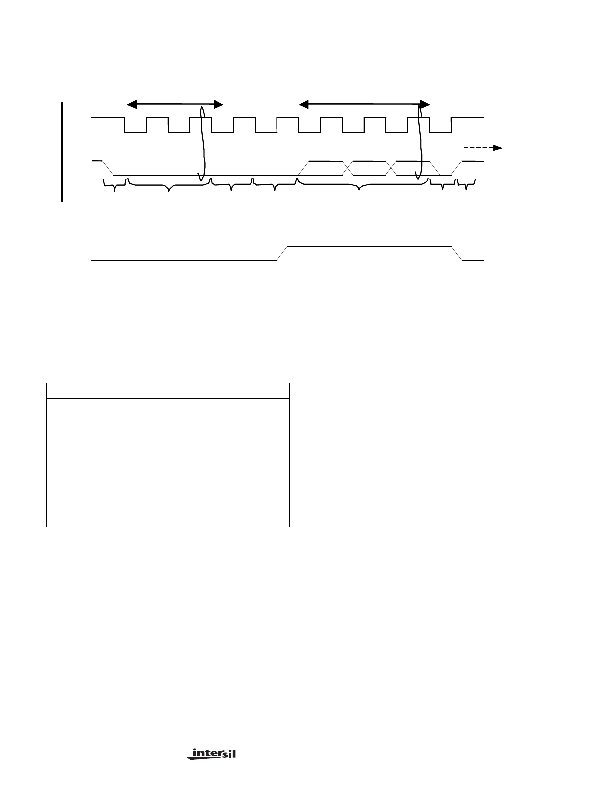
Startup Process
ISL6580 Enumeration
After power-up of the system, each installed ISL6580 is
polled for its existence. This procedure involves the
Controller to assert the PWM signal for a specific Power IC.
If the specified Power IC is present, it will assert its signal to
acknowledge seeing its PWM asserted. This sequence is
repeated for each Power IC that may be in the system. This
process is known as Device Polling.
After this initial PWM polling is complete, the serial interface
of each Power IC has to be configured with a device ID to be
able to respond to serial commands later. This procedure
involves issuing a “config call” which is to send a serial write
command to global device ID ‘0’. During the data portion of
the cycle, the Power IC to be configured has its PWM signal
asserted by the Controller. This action allows the data bits
that are sent from the Controller to be shifted into a device ID
register within the Power IC. This process is known as
Enumeration.
During enumeration, the address on the serial bus for each
ISL6580 is uniquely defined according to Table 6. If an
address acknowledge bit is not returned, the device is not
used because it is either not present or not functional. The
PWM signals are used to enable address writing to each
ISL6580. Fault processing is disabled during enumeration.
13
Page 14
SCLK
SCLK
SDATA
SDATA
ISL6590
Address Cycle Data Cycle
Address Cycle Data Cycle
10 clocks 8 Clocks
10 clocks 8 Clocks
Repeat for N-1 devices
Repeat for N-1 devices
Start
Start
"0000000000"
"0000000000"
PWM1 MHz Power IC 1 ID register enable
PWM1 MHz Power IC 1 ID register enable
("ID" register enable)
("ID" register enable)
MHz Power IC Configuration Process
First the master will initiate “config call” by sending a “10’h00” address
All of the slaves should “ACK” because every MHz Power IC register contains 0” after reset
The ID is then sent out during the data cycle.
The process is repeated until all (N) of the devices are configured.
TABLE 10. SERIAL BUS ID MAPPING
BSB ID DESCRIPTION
00h “config call”
01h Power IC 1
02h Power IC 2
03h Power IC 3
04h Power IC 4
05h Power IC 5
06h Power IC 6
09-1Fh Reserved
ISL6580 Calibration
Prior to calibration, the status of each ISL6580 is checked.
The input supply voltage is checked by polling the status of
the under-voltage lockout in the status registers of the
ISL6580s. Other faults are also checked. If a fault is
detected during or after calibration, the system state may be
frozen while fault processing takes over to resolve the error.
To calibrate the voltage ADC, the VID is set to the same
voltage as the external VID setting. Voltage ADC calibration
is initiated by setting the device that is hard wired for
Ack R/W
Ack R/W
Directio
Directio
FIGURE 11. ENUMERATION TIMING DIAGRAM
ID for Power IC 1
ID for Power IC 1
n
n
ISL6580 Softstart
The system is slowly brought out of the no output voltage
open loop state by sending a small PWM pulse width to the
ISl6580s. A fixed time period and step size is used to bring
the output voltage into the lower range of the voltage ADC.
Once the voltage ADC begins readin g vo lt ag e , a fi xed V
step size is used (25mV). After each V
performed, the output voltage must settle within a +/(V
/2) mV window of the specified VID voltage before
step
stepping to the next output voltage setting. The stepping
continues until the final voltage is reached.
Power On Reset
The ISL6590 controller performs a Power On Reset function
internally. It holds all internal logic in a reset state until the
Vdd (3.3V) exceeds a threshold. While in the reset state all
PWM and NDRIVE signals are held at ground and all
MOSFETs are OFF.
Duty Cycle Limit
The ISL6590 limits the on time of the upper FETs. The
system designer can set the maximum ON time with
PowerCode software The value is put in as a percentage. If
the duty cycle reaches this percentage, the top side FET
turns off until the next cycle.
Regulation mode into calibration mode. This should be
device #1. During calibration, any offset voltage internal to
the ADC is output on the ERR serial line. The error is stored
in the non-volatile memory. Then the ISL6590 changes
themode of the ISL6580 to normal operation and calibration
is complete.
Ack Stop Configcall
Ack Stop Configcall
step
step
step is
14
Page 15

Loop Compensation
Any closed loop system must be designed to insure stability
(prevent oscillation) and provide correct response to external
events such as load transients. The output of a buck
regulator has an inherent, low pass filter formed by the
output inductor(s), output capacitance and their ESRs
(Equivalent Series Resistance). Figure 12 shows a typical
gain and phase plot of output inductors, capacitors and ESR.
ISL6590
0
-10
-20
-30
-40
-50
-60
Plant Gain (in DB)
-70
-80
-90
1 10 100 1000 10000
Frequency (in KHz)
FIGURE 12. FREQUENCY RESPONSE OF THE OUTPUT
INDUCTORS AND CAPACITORS
Plant Gain
Phase
0
-20
-40
-60
-80
-100
Phase (in Degrees)
-120
-140
Above the resonant frequency of the output LC filter (10kHz
in this case) the gain falls at a rate of 40dB/decade and the
phase shift approaches –180 degrees. At a frequency
above the F = 1/(2πC*ESR) = 500kHz in this case) the gain
slope changes to –20dB/decade and the phase shift
approaches –90 degrees In a closed loop control system,
the output is subtracted from a reference voltage to produce
an error voltage. The error voltage is amplified and fed to
the output stage. In a buck regulator the output stage
consists of a Pulse Width Modulator (PWM), switching
transistors (typically MOSFETs), series inductor(s) and
output capacitors. High gain feedback reduces variation in
the output due to changes in input voltage, load current and
component values. However, high gain at high frequencies
can cause excessive over shoot in response to transients ( if
phase shift > 120 degrees and gain > 0dB ) or oscillation ( if
phase shift > 180 degrees and gain > 0dB ). The trade off in
designing the loop compensation is to achieve fast response
to transients without excessive overshoot or oscillation.
FIGURE 13. TYPICAL ANALOG VOLTAGE LOOP BLOCK
FIGURE 14. DIGITAL CONTROL LOOP BLOCK DIAGRAM
DIAGRAM
The ISL6580 subtracts a reference from the output voltage
to produce an error voltage. It converts the error voltage to a
6 bit digital number and sends it to the ISL6590 controller.
The controller processes the error number numerically to
provide gain (P
phase lead (D
roportional), phase lag (Integration) and
erivative) functions. This forms the digital PID
control.
15
FIGURE 15. TYPICAL ANALOG ERROR AMPLIFIER AND
COMPENSATION
Page 16
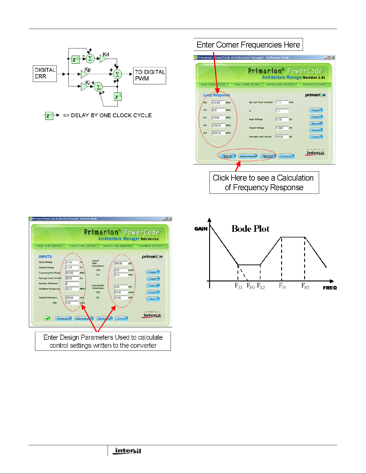
Adjusting The Digital PID
FIGURE 16. DIGITAL PID COMPENSATOR
Frequency response of the digital PID compensator is
determined by the Kp, Ki, Kd factors. These factors are
stored in nonvolatile memory and are loaded in the controller
at power on reset. The system designer sets the PID
compensators frequency response using user interface
software. The designer enters the frequencies of the
desired poles and zeros and user interface software
calculates the Kp, Ki and Kd factors. the software will
calculate and display the frequency response of the
feedback and the closed loop system.
ISL6590
FIGURE 18. SMALL SIGNAL DESIGN WINDOW
FIGURE 17. DESIGN PARAMETER INPUT WINDOW
16
FIGURE 19. BODE PLOT
F
= Frequency of first zero
Z1
= Frequency of second zero
F
Z2
FP0 = Gain * frequency of first pole (A
DC*F P0
)
FP1 = Frequency of second pole
RP2 = External Resistor used for third pole
CP2 = External Capacitor used for third pole
FP2 = 1 / (2 * π* RP2 * CP2 )
The software will calculate the frequency response of the
PID controller and the closed loop system as in figures 20
and 21 below.
Primarion is a registered trademark of Primarion, Inc. Primarion PowerCode is a trademark of Primarion, Inc
Page 17

ISL6590
60
50
40
30
20
Feedback Gain (in DB)
10
0
1 10 100 1000 10000
Frequency (in KHz)
Compensation
Phase
0
-10
-20
-30
-40
-50
-60
-70
-80
-90
FIGURE 20. PID COMPENSATOR FREQUENCY RESPONSE
60
40
20
0
-20
-40
-60
Loop Gain (in DB)
-80
-100
-120
1 10 100 1000 10000
Loop
Phase
Frequency (in KHz)
400
350
300
250
200
150
100
50
0
-50
Phase (in Degrees)
Phase (in Degrees)
slightly below 180 degrees at the cross over frequency, the
loop will respond to transients with overshoot and ringing.
Loop phase shift between 90 and 120 degrees at the cross
over frequency (Phase margin = 60 to 90 degrees) results in
little or no over shoot and ringing. Large phase margins
(>90 degrees) result in slower transient response.
Time Domain
It is recommended to place the first zero (FZ1) at the
resonant frequency of the output inductors and capacitors (F
= 1/(2π√LC = 10kHz in this case). Then increase F
F
to minimize response time over (under) shoot and
P0
ringing. The first microseconds of transient response are
primarily dependant on the ESR and ESL of the output
capacitors. After the affects of ESL and ESR pass the loop
must control the response.
Z2
and
FIGURE 21. FREQUENCY RESPONSE OF THE CLOSED LOOP
Compensation Methodology
Due to the user interface software interface, it is very easy to
change the frequency compensation and see the resulting
performance on a scope or network analyzer. Transient
response is viewed by applying a transient load and
monitoring the output voltage with a scope. Frequency
response is viewed by placing a small resistor between the
output and the feed back network, applying a small sine
wave at the input to the feed back network and measuring
the amplitude and phase shift of the resulting sine wave on
the output. Sweeping the frequency produces plots similar
to those above.
Frequency Domain
It is recommended to place the first zero (FZ1) at the
resonant frequency of the output inductors and capacitors (F
= 1/(2π√LC) = 10kHz in this case). Then increase F
F
to maximize DC gain and the frequency at which gain
P0
drops below 0dB while keeping the phase margin above 60
degrees. Phase Margin is the difference between 180
degrees and the phase shift of the loop at the frequency
where the gain drops below 0dB (cross over frequency). If
the loops phase shift reaches 180 degrees and has gain
equal to or greater than 0dB, it acts as positive feed back
and the loop will oscillate. Even if the loops phase shift is
Z2
and
FIGURE 22. TYPICAL RESPONSE TO A LOAD TRANSIENT
User Interface Software
The ISL6590 controller and the ISL6580 intelligent power
stage have programmable values that can be changed using
the User Interface Software. The loop configuration and
system performance is adjusted using the software. The use
of the software allows the engineer to evaluate the system
performance without having to physically change
components on the board. Primarion PowerCode user
interface software (provided by Intersil and our partner
Primarion).
Below are screen shots showing data entry points, pull down
menus, buttons for help and a tutorial. The user interface
software allows the designer to adjust the load line,
frequency response, ATR and protection modes.
17
Page 18

ISL6590
FIGURE 23. PRIMARION POWERCODE LOADLINE AND ATR
SETTINGS
FIGURE 24. PRIMARION POWERCODE LOOP RESPONSE
SETTINGS
FIGURE 25. PRIMARION POWERCODE MONITOR WINDOW
FIGURE 26. PRIMARION POWERCODE DESIGN INPUTS
18
FIGURE 27. PRIMARION POWERCODE DUTY CYCLE LIMIT
SELECTION
Page 19

ISL6590
Register Description Tables
TABLE 11. ISL6590 MEMORY MAP
R/W/S
ADDRESS RANGE NAME
VOLATILE MEMORY
0000 - 01FF General Control Registers R/W/Ws
0000 Part Number (ASCII character #1) R 8
0001 Part Number (ASCII character #2) R 8
0002 Part Number (ASCII character #3) R 8
0003 Part Number (ASCII character #4) R 8
0004 Version Number (ASCII) R8
0005 Vendor Name (ASCII character #1) R 8
0006 Vendor Name (ASCII character #2) R 8
0007 Vendor Name (ASCII character #3) R 8
0008 Vendor Name (ASCII character #4) R 8
0009 Reserved
000A SPI Memory Status Register R3
000B Reserved
000C Serial Polling Enable R/W 1
000D Reserved
000E System Status (LSB) R/Ws 8
000F System Status (MSB) R/Ws 8
0010 Oscillator-In Frequency (LSB) R 8
0011 Oscillator-In Frequency (MSB) R 8
0012 State Control Status (LSB) R/Ws 8
0013 State Control Status (MSB) R/Ws 8
0014 Reserved
0015 Reserved
0016 – 00EF Reserved
00F0 Scratchpad R/W 8
00F1 – 00FF Reserved
0100 - 01FF Reserved
0200 - 02FF Control/Status Registers R/W/Ws
0200 Reserved
0201 Feedback Loop Control R/W 6
0202 Open Loop PID (LSB) R/W 8
0203 Open Loop PID (MSB) R/W 7
0204 – 0205 Reserved
0206 ATR Control
0207 Phases Used
0208 Phase Enables
209 Reserved
(NOTE 1)
R/W 4
R4
R/W 8
(BITS)
1
SIZE (bits)
1
Size (bits)
SIZE
19
Page 20

ISL6590
TABLE 11. ISL6590 MEMORY MAP (Continued)
R/W/S
ADDRESS RANGE NAME
020A VID_IN_SOFT R/W 6
020B Alive Found R8
020D Reserved
020E VCODE_IN R8
020F VCODE_OUT R/W 8
0210 Enumeration Control R/W 3
0211 Enumeration Done R4
0212 VID_IN (from VID pins) R6
0213 OUTEN (from OUTEN pin) R1
0214 PWRGD R1
0215 VID_OUT R7
0216 Voltage Error R6
0217 Average Peak Channel Current R 6
0218 Overload R8
0219 AVP Offset R8
021A Voltage Calibration Offset R/W 5
021B Regulated R1
021C – 21F Reserved
0220 Peak Channel Current – Phase 1 R 6
0221 Peak Channel Current – Phase 2 R 6
0222 Peak Channel Current – Phase 3 R 6
0223 Peak Channel Current – Phase 4 R 6
0224 Peak Channel Current – Phase 5 R 6
0225 Peak Channel Current – Phase 6 R 6
0226 Peak Channel Current – Phase 7 R 6
0227 Peak Channel Current – Phase 8 R 6
0228 – 022F Reserved
0230 On Time – Phase 1 (upper 8 bits) R 8
0231 On Time – Phase 2 (upper 8 bits) R 8
0232 On Time – Phase 3 (upper 8 bits) R 8
0233 On Time – Phase 4 (upper 8 bits) R 8
0234 On Time – Phase 5 (upper 8 bits) R 8
0235 On Time – Phase 6 (upper 8 bits) R 8
0236 On Time – Phase 7 (upper 8 bits) R 8
0237 On Time – Phase 8 (upper 8 bits) R 8
0238 – 02FF Reserved
0300 - 03FF Reserved
0400 – 07FF Broadcast Write Memory Map R/W/Ws
0400 Reserved
(NOTE 1)
1
Size (bits)
SIZE
(BITS)
20
Page 21

ISL6590
TABLE 11. ISL6590 MEMORY MAP (Continued)
R/W/S
ADDRESS RANGE NAME
0401 Reserved
0402 HFWND (High ATR Window) W 4
0403 LFWND (Low ATR Window) W4
0404 VID (7 bit Voltage Identification) W 7
0405 ILIM (Current Limit) W2
0406 TSD (Thermal Shutdown) W3
0407 Reserved
0408 TEST W8
0409 ENABLE1 (Block Enables LSB) W 8
040A ENABLE2 (Block Enables MSB) W 3
040B SPARE1 W8
040C SPARE2 W8
040D – 041F Reserved
Device 1 Memory Map R/W/Ws
0420 Reserved
0421 Bus ID R4
0422 HFWND (High ATR Window) R/W 4
0423 LFWND (Low ATR Window) R/W 4
0424 VID (7 bit Voltage Identification) R/W 7
0425 ILIM (Current Limit) R/W 2
0426 TSD (Thermal Shutdown) R/W 3
0427 FAULT (Fault Status) R6
0428 TEST R/W 8
0429 ENABLE1 (Block Enables LSB) R/W 8
042A ENABLE2 (Block Enables MSB) R/W 3
042B SPARE1 R/W 8
042C SPARE2 R/W 8
0440 – 07FF Device n to 31 Memory Map (structure as Device 1)
NON-VOLATILE MEMORY
0800 – 09FF General Settings R/W/Ws
0800 NVMEMCODE R/W 8
0801 Serial Clock Divider R/W 3
0802 VID_IN Table Select R/W 2
0803 VID_OUT Table Select R/W 2
0804 OffOn Non-Overlap Driver Control R/W 4
0805 OnOff Non-Overlap Driver Control R/W 4
0806 Duty Limit R/W 8
0807 System Configuration R/W 3
0808 Reserved R/W 5
(NOTE 1)
(BITS)
1
SIZE (bits)
1
Size (bits)
SIZE
21
Page 22

ISL6590
TABLE 11. ISL6590 MEMORY MAP (Continued)
R/W/S
ADDRESS RANGE NAME
0809 A/D ID R/W 5
080A WCOMP ID R/W 5
080B OUVP ID R/W 5
080C MG Poll Priority R/W 7
080D State Control R/W 6
080E Reserved R/W 2
080F Phases to be Used R/W 8
0810 POR Wait R/W 5
0811 Regulation Window R/W 6
0812 Regulation Time R/W 8
0813 Voltage Calibration Maximum R/W 6
0814 Reserved R/W 8
0815 Startup Fault Mask R/W 7
0816 Startup Enables 1 R/W 8
0817 Startup Enables 2 R/W 5
0818 Active Fault Mask R/W 7
0819 Active Enables 1 R/W 8
081A Active Enables 2 R/W 5
081B Active Feature Mask R/W 1
081C Reserved
081D Current Limit R/W 6
081E – 083F Reserved
0840 ATR Exit Delay R/W 5
0841 ATR Count Max (LSB) R/W 8
0842 ATR Count Max (MSB) R/W 1
0843 PVID Offset R/W 4
0844 – 086F Reserved
0870 – 08FF Reserved
Address Range General Control Registers R/W/Ws1 Size (bits)
Phase # Independent Compensation Parameters
0900 Kp AVP R/W 8
0901 Kd AVP R/W 8
0902 Kp PID R/W 6
0903 Ki PID R/W 8
0904 Kd Transient Recovery R/W 8
0905 Vos AVP R/W 6
0906 Ios AVP R/W 8
0907 Kfp PID R/W 6
0908 Kfd PID R/W 6
(NOTE 1)
SIZE
(BITS)
22
Page 23

ISL6590
TABLE 11. ISL6590 MEMORY MAP (Continued)
R/W/S
ADDRESS RANGE NAME
Phase # Dependent Compensation Parameters
0909 K Current Balancing R/W 8
090A Kd PID R/W 8
090B HFWND R/W 4
090C LFWND R/W 4
090D OUVPLF R/W 4
090E OOVPHF R/W 4
090F ILIM (not phase # dependent) R/W 2
0910 Reserved
0911 Reserved
0912 Switching Frequency Phases=1 (LSB) R/W 8
0913 Switching Frequency Phases=1 (MSB) R/W 4
0914 Switching Frequency Phases=2 (LSB) R/W 8
0915 Switching Frequency Phases=2 (MSB) R/W 4
0916 Switching Frequency Phases=3 (LSB) R/W 8
0917 Switching Frequency Phases=3 (MSB) R/W 4
0918 Switching Frequency Phases=4 (LSB) R/W 8
0919 Switching Frequency Phases=4 (MSB) R/W 4
091A Switching Frequency Phases=5 (LSB) R/W 8
091B Switching Frequency Phases=5 (MSB) R/W 4
091C Switching Frequency Phases=6 (LSB) R/W 8
091D Switching Frequency Phases=6 (MSB) R/W 4
091E Switching Frequency Phases=7 (LSB) R/W 8
091F Switching Frequency Phases=7 (MSB) R/W 4
0920 Switching Frequency Phases=7 (LSB) R/W 8
0921 Switching Frequency Phases=7 (MSB) R/W 4
0922 – 093F Reserved
0940 Custom VID2VCODE0 LUT Entry
0941 – 097F Custom VID2VCODE1 to VID2VCODE63 LUT Entries
0980 – 09FF Reserved for User R/W/Ws1SIZE (bits)
0A00 – FFFF Reserved
TABLE 12. SECOND SOURCE INFORMATION
o
PART NUMBER TEMP. (
Primarion PX3530 0 to 85 64 Ld QFN L64.9x9
C) PACKAGE PKG. NO
(NOTE 1)
R/W 8
R/W 8
SIZE
(BITS)
All Intersil U.S. products are manufactured, assembled and tested utilizing ISO9000 quality systems.
Intersil Corporation’s quality certifications can be viewed at www.intersil.com/design/quality
Intersil products are sold by description only. Intersil Corporation reserves the right to make changes in circuit design, software and/or specifications at any time without
notice. Accordingly, the reader is cautioned to verify that data she ets are current before placin g orders. Information furn ished by Intersil is believed to be accurate and
reliable. However, no responsibility is assumed by Intersil or its subsidiaries for its use; nor for any infringements of patents or other rights of third parties which may result
from its use. No license is granted by implication or othe rwise under any patent or patent righ ts of Intersil or its subsidiaries.
For information regarding Intersil Corporation and its products, see www.intersil.com
23
Page 24

ISL6590
Quad Flat No-Lead Plastic Package (QFN)
Micro Lead Frame Plastic Package (MLFP)
0.10
2X
2X
SEATING
PLANE
(DATUM B)
(DATUM A)
NX L
INDEX
AREA
C
4X P
6
INDEX
AREA
B
4X
4X P
2X
A
N
6
1
2
3
C0.10
A
0
C
4X b
3
2
1
N
D
9
TOP VIEW
SIDE VIEW
5
0.10 BAMC
D2
e
(Nd-1)Xe
REF.
BOTTOM VIEW
NX b
5
SECTION "C-C"
SCALE: NONE
D1
78
D2
2
D/2
D1/2
NX k
N
A1
E1/2
A3
E2/2
A0.10
C
2X
0.10
C
E/2
E
E1
9
B
A2
A
/
0.10
C
/
0.08 C
A1
(Ne-1)Xe
E2
REF.
7
8
L64.9x9-S
64 LEAD QUAD FLAT NO-LEAD PLASTIC PACKAGE
MILLIMETERS
SYMBOL
A 0.70 0.75 0.80 A1 - - 0.05 A2 - 0.50 - -
B
A3 0.25 REF -
b 0.18 0.20 0.30 5, 8
D 9.00 BSC D1 8.75 BSC D2 3.64 3.74 3.84 7, 8
E 9.00 BSC E1 8.75 BSC E2 3.64 3.74 3.84 7, 8
e 0.50 BSC -
k0.25 - - -
L 0.30 0.40 0.50 8
L1 - - 0.15 9
N642
Nd 16 3
Ne 16 3
P- -0.50-
θ --8-
NOTES:
1. Dimensioning and tolerancing conform to ASME Y14.5-1994.
2. N is the number of terminals.
3. Nd and Ne refer to the number of terminals on each D and E.
4. All dimensions are in millimeters. Angles are in degrees.
5. Dimension b applies to the metallized terminal and is measured
between 0.15mm and 0.30mm from the terminal tip.
6. The configuration of the pin #1 identifier is optional, but must be
located within the zone indicated. The pin #1 identifier may be
either a mold or mark feature.
7. Dimensions D2 and E2 are for the exposed pads which provide
improved electrical and thermal performance.
8. Nominal dimensions are provided to assist with PCB Land Pattern
Design efforts, see Intersil Technical Brief TB389.
9. Depending on the method of lead termination at the edge of the
package, a maximum 0.15mm pull back (L1) maybe present. L
minus L1 to be equal to or greater than 0.3mm.
NOTESMIN NOMINAL MAX
Rev. 0 04/03
TERMINAL TIP
C
L
e
FOR EVEN TERMINAL/SIDE
24
9
L
L1
 Loading...