

查询ISL6571供应商
®
ISL6571
Data Sheet April 18, 2005
Complementary MOSFET Driver and
Synchronous Half-Bridge Switch
The Intersil ISL6571 provides a new approach for
implementing a synchronous rectified buck switching
regulator. The ISL6571 replaces two power MOSFETs, a
Schottky diode, two gate drivers and synchronous control
circuitry. Its main applications address high-density power
conversion circuits including multiphase-topology computer
microprocessor core power regulators, ASIC and memory
array regulators, etc. Another useful feature of the ISL6571
is the compatibility with three-state input control: left open,
the PWM input turns off both output drives. The ISL6571
operates in continuous conduction mode reducing EMI
constraints and enabling high bandwidth operation.
Ordering Information
TEMP.
PART NUMBER
ISL6571CR* 0 to 70 68 Ld 10x10 QFN L68.10x10A
ISL6571CRZ*
(See Note)
ISL6571EVAL1 Evaluation Board
*Add “-T” suffix for tape and reel.
NOTE: Intersil Pb-free products employ special Pb-free material
sets; molding compounds/die attach materials and 100% matte tin
plate termination finish, which are RoHS compliant and compatible
with both SnPb and Pb-free soldering operations. Intersil Pb-free
products are MSL classified at Pb-free peak reflow temperatures that
meet or exceed the Pb-free requirements of IPC/JEDEC J STD-020.
RANGE (°C) PACKAGE
0 to 70 68 Ld 10x10 QFN
(Pb-free)
PKG.
DWG. #
L68.10x10A
FN9082.4
Features
• Improved Performance over Conventional Synchronous
Buck Converter using Discrete Components
• Optimal Deadtime Provided by Adaptive Shoot-Through
• Switching Frequency up to 1MHz
- High-Bandwidth, Fast Transient Response
- Small, Low Profile Converters
• Reduced Connection Parasitics between Discrete
Components
- Low Electromagnetic Emissions
• Low Profile, Low Thermal Impedance Packaging
- High Power Density Applications
• QFN Package:
- Compliant to JEDEC PUB95 MO-220
QFN - Quad Flat No Leads - Package Outline
- Near Chip Scale Package footprint, which improves
PCB efficiency and has a thinner profile
• Pb-Free Available (RoHS Compliant)
Applications
•
Multiphase Power Regulators
•
Low-Voltage Switchmode Power Conversion
• High-Density Power Converters
1
CAUTION: These devices are sensitive to electrostatic discharge; follow proper IC Handling Procedures.
1-888-INTERSIL or 1-888-352-6832
| Intersil (and design) is a registered trademark of Intersil Americas Inc.
All other trademarks mentioned are the property of their respective owners.
Copyright Intersil Americas Inc. 2003-2005. All Rights Reserved

ISL6571
Pinout
PHASE
PHASE
PHASE
PHASE
PHASE
PHASE
PHASE
PHASE
PHASE
PHASE
PHASE
PHASE
PHASE
PHASE
PHASE
PHASE
PHASE
PGND
PGND
PGND
PGND
67666564636261
68
1
2
3
4
5
6
7
8
9
10
11
12
13
14
15
16
17
18
19202122232425
ISL6571 (QFN) TOP VIEW
PGND
PGND
PGND
PGND
PGND
LGATE1
PHASEPHASE
58
59
60
69
PHASE
28
27
26
PVCC
56
NC
55
71
GND
70
VIN
VCC
54
GND
57
2930313233
LGATE
NC
52
53
NC51
50
GND
49
NC
48
PWM
47
BOOT
GND
46
45
PHASE
44
VIN
43
VIN
42
VIN
41
VIN
VIN
40
VIN
39
38
VIN
VIN
37
36
VIN
VIN
35
34
NC
NC
NCNCNC
NC
NC
NC
NC
NC
VIN
VIN
VIN
VIN
VIN
VIN
2
FN9082.4
ISL6571
BOOT
UFET
VIN
DRIVE1
PVCC
PHASE
GATE
PVCC
CONTROL
LGATE
LFET
PGND
LGATE1
DRIVE2
VCC
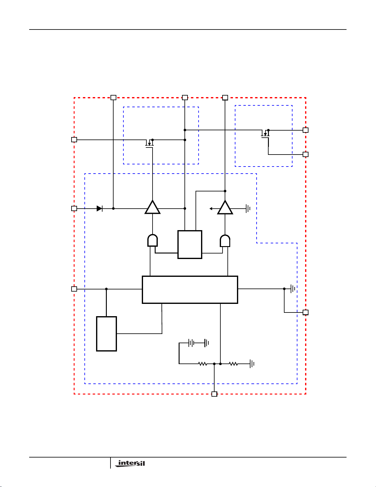
FIGURE 1. BLOCK DIAGRAM
LOGIC
CONTROL
GND
5V
+
-
POWER-ON
RESET (POR)
10K
PWM
10K
3
FN9082.4

+12VIN
+12VIN
+5VIN
PWM
ISL6571
CONTROL
AND
DRIVERS
ISL6571
FIGURE 2. SIMPLIFIED POWER SYSTEM DIAGRAM
L
IN
C
BOOT
L
OUT
C
OUT
V
OUT
+5VIN
POWER
GOOD
C
+
VCC
PWM
PVCC
BOOT
VIN
U2
ISL6571
GND
PVCC
U3
PHASE
PGND
BOOT
VIN
PHASE
18
17
19
PWM4
ISEN4
PGOOD
20
VCC
PWM1
ISEN1
PWM2
ISEN2
LGATE1
LGATE
15
16
14
13
VCC
PWM
ISL6571
LGATE1
U1
HIP6301
8
FS/DIS
R
FS
PWM3
ISEN3
11
12
LGATE
GND
PGND
IN1
C
BOOT1
L
OUT1
R
SNS1
C
+
IN2
C
BOOT2
L
OUT2
V
OUT
R
SNS2
C
OUT
+
R
OFFSET
COMP
VSEN
10
FB
6
7
C2
C1
R2
VCC
PWM
PVCC
U4
BOOT
VIN
ISL6571
GND
PHASE
PGND
LGATE1
LGATE
R1
5
VID0
4
VID1
3
VID2
2
VID3
1
VID4
GND
9
C
+
IN3
C
BOOT3
L
OUT3
R
SNS3
FIGURE 3. TYPICAL APPLICATION
4
FN9082.4

ISL6571
Absolute Maximum Ratings Thermal Information
Bias Supply Voltage, VCC . . . . . . . . . . . . . . . . . . . . . . . . . . . . .+15V
Driver Supply, PVCC . . . . . . . . . . . . . . . . . . . . . . . . . . . . . . . +10.5V
Conversion Voltage, VIN . . . . . . . . . . . . . . . . . . . . . . . . . VCC+0.3V
DRIVE1 Voltage, V
Input Voltage, PWM . . . . . . . . . . . . . . . . . . . . . . . . GND -0.3V to 7V
BOOT
- V
. . . . . . . . . . . . . . . . . . . . . .+15V
PHASE
ESD Classification . . . . . . . . . . . . . . . . . . . . . . . . . . . . . . . . Class 2
Recommended Operating Conditions
Control and Conversion Voltage, VCC, VIN. . . . . . . . . . +12V ±10%
MOSFET Bias Supply, PVCC . . . . . . . . . . . . . . . . . . . +5V to +10V
Ambient Temperature Range . . . . . . . . . . . . . . . . . . . . . 0°C to 70°C
Junction Temperature Range . . . . . . . . . . . . . . . . . . . . 0°C to 125°C
CAUTION: Stresses above those listed in “Absolute Maximum Ratings” may cause permanent damage to the device. This is a stress only rating and operation of the
device at these or any other conditions above those indicated in the operational sections of this specification is not implied.
NOTE:
is measured with the component mounted on a typical application PCB. A separate θ
1. θ
JC
pads (#69, 70, 71). Each value should be used in combination with the power dissipated by only the individual die mounted on that pad.
Electrical Specifications Recommended Operating Conditions, Unless Otherwise Noted. Refer to Figures 1, 2 and 3
PARAMETER SYMBOL TEST CONDITIONS MIN TYP MAX UNITS
SUPPLY CURRENT
Nominal Bias Supply Current I
VCC
POWER-ON RESET
Rising VCC Threshold 9.70 9.95 10.40 V
VCC Threshold Hysteresis -2.40- V
MOSFET DRIVER
Input Impedance Z
IN
PWM Rising Threshold - - 3.80 V
PWM Falling Threshold 1.30 - - V
PWM-to-PHASE Low-to-High Propagation
Delay
PWM-to-PHASE High-to-Low Propagation
t
PLH
t
PHL
Delay
Shutdown Window 1.60 - 3.40 V
Shutdown Holdoff Time t
SH
UPPER MOSFET (UFET)
Drain-to-Source ON-State Resistance r
DS(ON)
ON-State Drain Current V
LOWER MOSFET (LFET)
Drain-to-Source ON-State Resistance r
DS(ON)
ON-State Drain Current V
PWM Open - 2.5 3.6 mA
V
- V
BOOT
V
- V
BOOT
- V
BOOT
V
= 5V 4.10 4.80 5.55 mΩ
PVCC
V
= 10V 3.40 4.05 4.70 mΩ
PVCC
= 5V 25 - - A
PVCC
Thermal Resistance (Typical, Note 1)
Pad 69 . . . . . . . . . . . . . . . . . . . . . . . . . . . . . . . . . . . 1.3
Pad 70 . . . . . . . . . . . . . . . . . . . . . . . . . . . . . . . . . . . 4.0
Pad 71 . . . . . . . . . . . . . . . . . . . . . . . . . . . . . . . . . . . 6.0
Maximum Junction Temperature . . . . . . . . . . . . . . . . . . . . . . . 125°C
Maximum Storage Temperature Range . . . . . . . . . . . -40°C to 125°C
Maximum Lead Temperature (Soldering 10s) . . . . . . . . . . . . . 300°C
value is provided for each of the three exposed die
JC
-5- kΩ
-80- ns
-56- ns
- 230 - ns
= 5V 12.8 13.5 18.2 mΩ
PHASE
= 10V 7.70 9.20 12.7 mΩ
PHASE
= 5V 25 - - A
PHASE
θ
JC
(°C/W)
5
FN9082.4

Typical Performance Curves/Setup
∆I
(p-p)
+12V
+5V
+12V
C
PVCC
C
VCC
VCC
PVCC
BOOT
VIN
LOUT
C
VIN
C
BOOT
ISL6571
V
R
OUT
OUT
(DS)ON
1.8
1.6
1.4
1.2
VGS = 10V
ID = 12A
1.0
NORMALIZED r
0.8
0.6
-25 0 25 50 100 125 150
75
Tj (°C)
FIGURE 5. UPPER MOSFET ON RESISTANCE vs
PWM
CONTROL
DRIVERS
ISL6571
GND
AND
PGND
PHASE
FIGURE 4. TYPICAL TEST CIRCUIT
C
L
OUT
OUT
V
OUT
R
OUT
TEMPERATURE
126
V
= 5V
PVCC
108
V
= 10V
PVCC
I
= 0A
PHASE
90
72
(mA)
54
PVCC
I
36
18
0
100 200 300 400 500 600 700 800 900 1000
SWITCHING FREQUENCY (kHz)
1.26
1.08
0.90
0.72
0.54
0.36
0.18
0
(W)
PVCC
P
1.6
VGS = 10V
1.4
(DS)ON
1.2
1.0
NORMALIZED r
0.8
0.6
ID = 20A
-25 0 25 50 100 125 150
Tj (°C)
75
FIGURE 6. BIAS SUPPLY CURRENT/POWER vs FREQUENCY FIGURE 7. LOWER MOSFET ON RESISTANCE vs
TEMPERATURE
4.00
V
= 5V
PVCC
I
= 12A
LOUT
3.50
L
= 1µH
OUT
3.00
2.50
DISSIPATED POWER (W)
2.00
1.50
200 500 700 900 1000
SWITCHING FREQUENCY (kHz)
600
800300 400
FIGURE 8. ISL6571 POWER DISSIPATION vs FREQUENCY
AT 12A
6
4.00
V
= 5V
PVCC
L
3.50
3.00
2.50
2.00
1.50
1.00
DISSIPATED POWER (W)
0.50
0
= 1µH
OUT
12Vin/1.5Vout
0 4.5 7.5 10.5 12.0
6.0
OUTPUT CURRENT (A)
9.01.5 3.0
750kHz
13.5
500kHz
300kHz
200kHz
15.0 16.5
FIGURE 9. ISL6571 POWER DISSIPATION vs CURRENT AT
200kHz, 300kHz, 500kHz, 750kHz
FN9082.4

ISL6571
Typical Performance Curves/Setup (Continued)
93
91
89
87
85
83
81
EFFICIENCY (%)
79
77
75
73
0 4.5 7.5 10.5 12.0
1.5 3.0
FIGURE 10. ISL6571 EFFICIENCY AT 200kHz, 300kHz, 500kHz, 750kHz
OUTPUT CURRENT (A)
Functional Pin Descriptions
VCC (Pin 54)
Provide a 12V bias supply for the driver IC to this pin. The
voltage at this pin is monitored for Power-On Reset (POR)
purposes.
PVCC (Pin 56)
Provide a well decoupled 5V to 10V bias supply at this pin.
The voltage at this pin is used to bias the gates of the
MOSFET switches.
GND (Pins 46, 50, 57, 71)
Ground pins for the driver IC. Connect these pins to the
circuit ground (plane) and to the PGND pins using the
shortest available paths.
PGND (Pins 60-68)
This is the source ground connection for the lower MOSFET
switches. Connect these pins to the circuit ground (plane)
and to the GND pins using the shortest available paths.
VIN (Pins 29-44, 70)
Connect these pins to the input voltage to be converted
down. Provide bulk and high-frequency decoupling
capacitors as close to these pins as feasible.
PHASE (Pins 1-17, 27, 45, 59, 69)
As a minimum, connect pin 69 to the output inductor. The
remainder of the PHASE pins may be tied to pin 69, left
open, or used for other connections. It is recommended pin
45 is connected to the bootstrap capacitor, C
BOOT (Pin 47)
This pin is connected to the PVCC pin through an internal
quasi-diode. Connect a bootstrap capacitor from this pin to
PHASE pin 45 (0.1µF recommended). This capacitor
BOOT
.
6.0
200kHz
300kHz
500kHz
750kHz
9.0
13.5
15.0 16.5
provides the bias for the upper MOSFET drive and the gate
charge for the upper MOSFET.
LGATE (Pin 53)
This pin is the output of the lower MOSFET drive. Connect
this pin to LGATE1 pin using the shortest available path.
LGATE1 (Pin 58)
This pin is connected to the gate of the lower MOSFET
switch. Connect this pin to LGATE pin using the shortest
available path.
PWM (Pin 48)
Connect this pin to the regulating controller’s PWM output.
Left open, this input will float to approximately 2.5V and
cause both MOSFET switches to be turned off. Applying 5V
to this input causes the upper MOSFET switch to be turned
on. A 0V applied to this input causes the lower MOSFET
switch to be turned on. The approximate input impedance of
this pin is 5kΩ.
NC (Pins 18-26, 28, 49, 51, 52, 55)
These pins are not internally connected.
Description
Bias Requirements
The on-board driver includes a Power-On Reset (POR)
function, which continually monitors the input bias supply.
The POR monitors the bias voltage (+12V
and enables the ISL6571 for operation immediately after it
exceeds the rising threshold. Upon the bias voltage’s drop
below the falling threshold, the IC is disabled and both
internal MOSFETs are turned off.
The output drivers are powered from the PVCC pin. For
proper functionality and driving capability, connect PVCC to
) at the VCC pin,
IN
7
FN9082.4

ISL6571
a suitable supply, 5V to 10V, no higher than the voltage
applied at the VCC pin. The higher the voltage applied at the
PVCC pin, the better the channel enhancement of the onboard power MOSFETs, but also the higher the power
dissipated inside the driver.
The down-conversion voltage applied at VIN cannot exceed
the bias voltage applied at VCC, but can be as low as
practically possible.
Operation
The ISL6571 combines two MOSFET transistors in a
synchronous buck power train configuration, along with a halfbridge MOSFET driver designed to control these two
MOSFETs. When reviewing the operational details, refer to
Figure 5 test setup.
With all requirements for operation met, a logic high signal
on the PWM pin causes the UFET to turn on, while a logic
low signal applied to the PWM pin causes LFET to turn on. If
the PWM input is driven within the shutdown window and
remains there for the minimum holdoff time specified (See
‘Electrical Specifications’), both MOSFETs are turned off.
PWM
GND
PHASE
GND
SH
PLH
t
FIGURE 11. PHASE RESPONSE TO PWM INPUT
PHL
t
t
At the transition between the on intervals of the two
MOSFETs, the internal driver acts in a ‘break-before-make’
fashion. Thus, the driver monitors the on device and turns on
the (previously) off device, following a short time delay after
the on MOSFET has turned off. This behavior is necessary
to insure the absence of cross-conduction (shoot-through)
amongst the two MOSFETs.
Application and Component Selection
Guidelines
Layout Considerations
MOSFETs switch very fast and efficiently. The speed with
which the current transitions from one device to another
causes voltage spikes across the interconnecting
impedances and parasitic circuit elements. The voltage
spikes can degrade efficiency, radiate noise into the circuit,
and lead to device overvoltage stress. Careful component
layout and printed circuit design minimizes the voltage
spikes in the converter. Consider, as an example, the turn-off
transition of the upper MOSFET. Prior to turn-off, the upper
MOSFET was carrying the full load current. During the turnoff, current stops flowing in the upper MOSFET and is picked
up by the lower MOSFET or Schottky diode. Any inductance
in the switched current path generates a large voltage spike
during the switching interval. Careful component selection,
tight layout of the critical components, and short, wide circuit
traces minimize the magnitude of voltage spikes.
The ISL6571 is the first step in such an efficient design. By
bringing the driver and switching transistors in close
proximity, most of the interconnect/layout parasitic
inductances are greatly reduced. However, these benefits
are nulled if the associated decoupling elements and other
circuit components are not carefully positioned and laid out
to help the ISL6571 realize its full potential. Figure 12 shows
one possible layout pattern, detailing preferred positioning of
components, land size/pattern, and via count. Figure 12 is
one of many possible layouts yielding good results; use it for
general illustration and guidance.
Locate the decoupling capacitors, especially the highfrequency ceramic capacitors, close to the ISL6571. To fully
exploit ceramic capacitors’ low equivalent series inductance
(ESL), insure their ground connection is made as close to
their grounded terminal as physically feasible. Figure 12
details via-in-pad (VIP) practices, where the via is placed on
the component’s landing pad, thus yielding the shortestpath, lowest ESL connection to the desired plane/island.
Via-in-pad design is very important to the layout of the
ISL6571, since it is an integral part of the thermal design
consideration. VIP not only provides the lowest ESL circuit
connections, but it is essential to the propagation of heat
from the internal dies to the ambient. The vias placed directly
underneath the bottom pads of the package provide a low
thermal impedance path for the heat generated inside the IC
to diffuse through the internal planes, as well as through
islands on the back side of the board. Layout with landing
pads for the bottom pads of the package devoid of vias is
possible (rather, with vias placed outside of the package
outline), but the thermal performance of such a layout would
be significantly reduced. Use the smallest diameter vias
available and avoid the use of thermal relief on the contacts
with internal planes; if thermal relief is mandatory on all vias,
design the thermal relief so that it voids the smallest possible
copper area around the vias (thus preserving thermal
conductivity and reducing electrical contact resistance).
A multi-layer printed circuit board is recommended. Dedicate
one solid layer for a ground plane and make all critical
component ground connections with vias to this layer.
Dedicate another solid layer as a power plane and break this
plane into smaller islands of common voltage levels. The
power plane should support the input power and output
power nodes.
8
FN9082.4

TO +12V
TO +5V
C
PVCC
C
VCC
TO PWM
C
BULK
C
PHASE
BOOT
VINGND
TO V
CHF (x2)
IN
ISL6571
Use the remaining printed circuit layers for small signal
wiring. The wiring traces from the surrounding application to
the ISL6571 should be sized according to their task. Thus,
small-signal traces, like the PWM signal or the ISEN
feedback (if used in conjunction with another Intersil
controller), only need be as wide as 5-10mils. Traces
carrying bias current should be larger, proportionately with
the current flowing through them; for example, traces
carrying PVCC current around 50-100mA would require
30-50mils. Generally, the best connections are the shortest,
enclosing the least amount of area possible. Similarly, from a
conduction requirement perspective, where vias are required
to carry current, use a via for each 2-3A of RMS current.
Bootstrap Requirements
The ISL6571 features an integrated boot element connected
between the PVCC and BOOT pins. A 0.1µF external
bootstrap capacitor is recommended.
TO L
OUT
KEY
ISLAND ON POWER PLANE LAYER
CONNECTING TRACES ON TOP/BOTTOM LAYERS
VIA CONNECTION TO OTHER PLANEs
FIGURE 12. PRINTED CIRCUIT BOARD POWER PLANES AND
ISLANDS
Use copper-filled polygons on the top and bottom circuit
layers for the PHASE node, but do not unnecessarily
oversize these particular islands. Since the PHASE node is
subject to very high dV/dt voltages, the stray capacitors
formed between these islands and the surrounding circuitry
or internal planes will tend to couple switching noise. On the
other hand, these islands have to be sufficiently large to offer
a good path to surrounding environment for the heat
produced inside the ISL6571.
Capacitor (Decoupling) Selection
To fully extract the benefits of a highly performant power
integrated circuit, the circuit elements surrounding it must
conform to the same high standards as the active power
element. As such, the capacitors used for high-frequency
decoupling of the ISL6571 should be good quality ceramic,
with a low ESR and ESL (X7R, X5R dielectric, and 0805 or
smaller footprints recommended); a minimum of two 1µF
capacitors are recommended. Bulk decoupling capacitor
technology is not restricted to ceramic, as electrolytic
capacitors are also suitable. For best results, select
capacitors based on the input RMS current draw of the
circuit, with a low ESL; distribute evenly amongst and place
them as close to the ISL6571 as possible.
ISL6571 DC-DC Converter Application
Circuit
Figure 13 shows an application circuit of a power supply for
a microprocessor computer system. For detailed information
on the circuit, including a Bill-of-Materials and circuit board
description, contact Intersil to order the evaluation kit
ISL6571EVAL1. Also see Intersil web page
(http://www.intersil.com).
All Intersil U.S. products are manufactured, assembled and tested utilizing ISO9000 quality systems.
Intersil Corporation’s quality certifications can be viewed at www.intersil.com/design/quality
Intersil products are sold by description only. Intersil Corporation reserves the right to make changes in circuit design, software and/or specifications at any time without
notice. Accordingly, the reader is cautioned to verify that data sheets are current before placing orders. Information furnished by Intersil is believed to be accurate and
reliable. However, no responsibility is assumed by Intersil or its subsidiaries for its use; nor for any infringements of patents or other rights of third parties which may result
from its use. No license is granted by implication or otherwise under any patent or patent rights of Intersil or its subsidiaries.
For information regarding Intersil Corporation and its products, see www.intersil.com
9
FN9082.4

+12VIN
+5VIN
POWER
GOOD
>
R
FS
ISL6571
L
IN
>
>
VCC
PWM
LGATE1
ISL6571
LGATE2
C
VCC1
20
VCC
R
PG
19
PGOOD
U1
PWM1
ISEN1
PWM2
ISEN2
PWM3
ISEN3
15
16
14
13
11
12
HIP6301
8
5
4
3
2
1
FS/DIS
VID0
VID1
VID2
VID3
VID4
GND
9
PWM4
ISEN4
COMP
VSEN
10
FB
18
17
6
C2
C1
7
R2
LGATE
VCC
PWM
LGATE1
ISL6571
LGATE2
LGATE
VCC
PWM
LGATE1
ISL6571
LGATE2
PVCC
U2
GND
PVCC
U3
GND
PVCC
U4
BOOT
VIN
PHASE
PGND
BOOT
VIN
PHASE
PGND
BOOT
VIN
PHASE
+
C
IN1
C
BOOT1
L
OUT1
R
SNS1
+
C
IN2
C
BOOT2
L
OUT2
+
C
C
BOOT3
OUT
L
OUT3
V
OUT
R
SNS2
C
+
IN3
ADDITIONAL
HIGH-FREQUENCY
DECOUPLING
C
VCC2-5
C
PVCC2-5
C
VIN2-5
C
OUT_HF
C
OUT_BULK
R
OFFSET
1 to each of VCC2-5
1 to each of PVCC2-5
2 to each of VIN2-5
varied HF mix to V
varied bulk mix to V
OUT
10
OUT
R3
C3
LGATE
R1
VCC
PWM
LGATE1
LGATE2
LGATE
GND
PVCC
U5
ISL6571
GND
PGND
BOOT
VIN
PHASE
PGND
FIGURE 13. TYPICAL ISL6571 APPLICATION CIRCUIT
R
SNS3
C
+
IN4
C
BOOT4
L
OUT4
R
SNS3
FN9082.4

ISL6571
Quad Flat No-Lead Plastic Package (QFN)
Micro Lead Frame Plastic Package (MLFP)
2X
C
A
5
0.10 C A B
7
A1
E1/2
M
8
NX k
E2/2
0.15
E1
A3 A1
(Ne–1)Xe
E2
8
A2
REF.
7
CC
E/2
C
2X
E
B
A
NX
E4
E3
L
e
0.15
2X
2X
SEATING
PLANE
INDEX
AREA
C
0.15
C
INDEX
AREA
NX L
8
6
4X P
4X P
6
A
N
1
2
3
B
C
A
θ
b
NX
3
2
1
N
C
L
D
D1
TOP VIEW
SIDE VIEW
D2
D4
69
e
(Nd–1)Xe
REF.
BOTTOM VIEW
NX b
D/2
D1/2
D2/2
D3
70
71
5
SECTION "C-C"
e
TERMINAL TIP
FOR ODD TERMINAL/SIDE FOR EVEN TERMINAL/SIDE
0.15
0.05
L68.10x10A
68 LEAD MICRO LEAD FRAME PLASTIC PACKAGE
(CUSTOMIZED WITH THREE EXPOSED PADS)
MILLIMETERS
SYMBOL
C
B
A- -0.90A1 - - 0.05 A2 - - 0.70 A3 0.20 REF -
b 0.18 0.23 0.30 5, 8
D 10.00 BSC D1 9.75 BSC D2 7.55 7.70 7.85 7, 8
D3 2.44 2.59 2.74 7, 8
D4 4.48 4.63 4.78 7, 8
E 10.00 BSC E1 9.75 BSC E2 7.55 7.70 7.85 7, 8
C
E3 2.44 2.59 2.74 7, 8
E4 4.48 4.63 4.78 7, 8
e 0.50 BSC -
k0.25 - - L 0.50 0.60 0.75 8
N682
Nd 17 3
Ne 17 3
P- -0.60-
θ --12-
NOTES:
1. Dimensioning and tolerancing per ASME Y14.5-1994.
2. N is the number of peripheral terminals. Exposed pads are
terminals 69, 70 and 71, as shown.
3. Nd is the number of terminals in the X direction, and Ne is the
number of terminals in the Y direction.
4. Controlling dimension: Millimeters. Angles are in degrees.
5. Dimension b applies to the plated terminal and is measured
between 0.20mm and 0.25mm from the terminal tip.
6. The configuration of the pin #1 identifier is optional, but must be
located within the zone indicated. The pin #1 identifier may be
either a molded or marked feature.
7. Dimensions D2/3/4 and E2/3/4 are for the three exposed pads
which provide improved electrical and thermal performance.
8. Nominal dimensions provided to assist with PCB Land Pattern
Design efforts, see Technical Brief TB389.
NOTESMIN NOMINAL MAX
Rev. 0 2/02
11
FN9082.4
 Loading...