®
ISL6566
Data Sheet
Three-Phase Buck PWM Controller with
Integrated MOSFET Drivers for VRM9,
VRM10, and AMD Hammer Applications
The ISL6566 three-phase PWM control IC provides a
precision voltage regulation system for advanced
microprocessors. The integration of power MOSFET drivers
into the controller IC marks a departure from the separate
PWM controller and driver configuration of previous multiphase product families. By reducing the number of external
parts, this integration is optimized for a cost and space
saving power management solution.
Outstanding features of this controller IC include
programmable VID codes compatible with Intel VRM9,
VRM10, as well as AMD Hammer microprocessors. A unity
gain, differential amplifier is provided for remote voltage
sensing, compensating for any potential difference between
remote and local grounds. The output voltage can also be
positively or negatively offset through the use of a single
external resistor.
A unique feature of the ISL6566 is the combined use of both
DCR and r
positioning (droop) and overcurrent protection are
accomplished through continuous inductor DCR current
sensing, while r
channel-current balance. Using both methods of current
sampling utilizes the best advantages of each technique.
Protection features of this controller IC include a set of
sophisticated overvoltage, undervoltage, and overcurrent
protection. Overvoltage results in the converter turning the
lower MOSFETs ON to clamp the rising output voltage and
protect the microprocessor. The overcurrent protection level
is set through a single external resistor. Furthermore, the
ISL6566 includes protection against an open circuit on the
remote sensing inputs. Combined, these features provide
advanced protection for the microprocessor and power
system.
current sensing. Load line voltage
DS(ON)
current sensing is used for accurate
DS(ON)
March 9, 2006
FN9178.4
Features
• Integrated Multi-Phase Power Conversion
- 1, 2, or 3-Phase Operation
• Precision Core Voltage Regulation
- Differential Remote Voltage Sensing
- ±0.5% System Accuracy Over Temperature
- Adjustable Reference-Voltage Offset
• Precision Channel Current Sharing
- Uses Loss-Less r
DS(ON)
Current Sampling
• Accurate Load Line Programming
- Uses Loss-Less Inductor DCR Current Sampling
• Variable Gate Drive Bias: 5V to 12V
• Microprocessor Voltage Identification Inputs
- Up to a 6-Bit DAC
- Selectable between Intel’s VRM9, VRM10, or AMD
Hammer DAC Codes
- Dynamic VID Technology
• Overcurrent Protection
• Multi-tiered Overvoltage Protection
• Digital Soft-Start
• Selectable Operation Frequency up to 1.5MHz Per Phase
• Pb-Free Plus Anneal Available (RoHS Compliant)
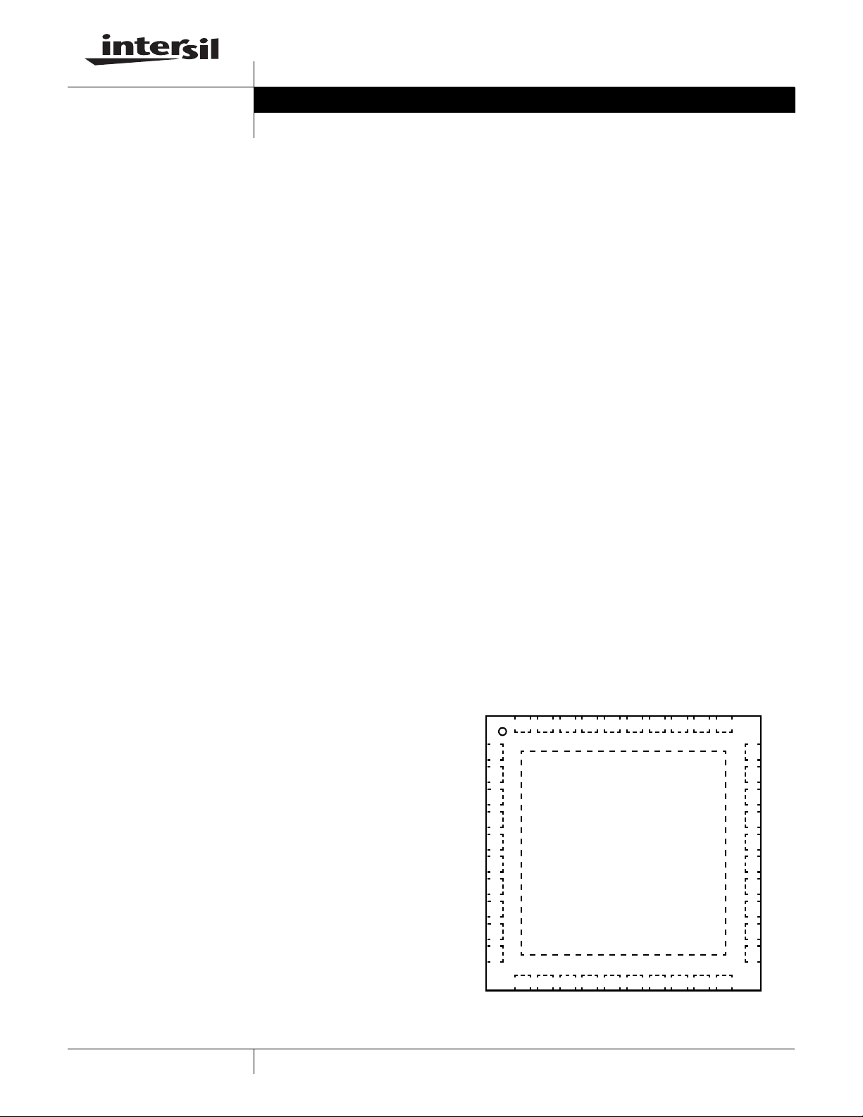
Pinout
ISL6566 (QFN)
TOP VIEW
VID3
VID4
VID1
VID0
VID12.5
VRM10
REF
OFS
VCC
COMP
FB
VDIFF
VID2
40
39 38 37 36 35 34 33 32 31
1
2
3
4
5
6
7
8
9
10
ENLL
FS
41
GND
PGOOD
LGATE1
PVCC1
ISEN1
UGATE1
30
29
28
27
26
25
24
23
22
21
BOOT1
PHASE1
PHASE2
UGATE2
BOOT2
ISEN2
PVCC2
LGATE2
PHASE3
BOOT3
11 12 13 14 15 16 17 18 19 20
IREF
VSEN
RGND
1
CAUTION: These devices are sensitive to electrostatic discharge; follow proper IC Handling Procedures.
1-888-INTERSIL or 1-888-468-3774
| Intersil (and design) is a registered trademark of Intersil Americas Inc.
All other trademarks mentioned are the property of their respective owners.
OCSET
Copyright Intersil Americas Inc. 2004-2006. All Rights Reserved
ISUM
ICOMP
LGATE3
ISEN3
PVCC3
UGATE3

Ordering Information
ISL6566ISL6566
PART
PART NUMBER
ISL6566CRR5184 ISL6566CR 0 to 70 40 Ld 6x6 QFN L40.6x6
ISL6566CR-TR5184 ISL6566CR 0 to 70 40 Ld 6x6 QFN Tape and Reel L40.6x6
ISL6566CRZR5184 (Note) ISL6566CRZ 0 to 70 40 Ld 6x6 QFN (Pb-free) L40.6x6
ISL6566CRZ-TR5184 (Note) ISL6566CRZ 0 to 70 40 Ld 6x6 QFN (Pb-free) Tape and Reel L40.6x6
ISL6566CRZAR5184 (Note) ISL6566CRZ 0 to 70 40 Ld 6x6 QFN (Pb-free) L40.6x6
ISL6566CRZA-TR5184 (Note) ISL6566CRZ 0 to 70 40 Ld 6x6 QFN (Pb-free) Tape and Reel L40.6x6
ISL6566IR ISL6566IR -40 to 85 40 Ld 6x6 QFN L40.6x6
ISL6566IR-T ISL6566IR -40 to 85 40 Ld 6x6 QFN Tape and Reel L40.6x6
ISL6566IRZ (Note) ISL6566IRZ -40 to 85 40 Ld 6x6 QFN (Pb-free) L40.6x6
ISL6566IRZ-T (Note) ISL6566IRZ -40 to 85 40 Ld 6x6 QFN (Pb-free) Tape and Reel L40.6x6
ISL6566IRZA (Note) ISL6566IRZ -40 to 85 40 Ld 6x6 QFN (Pb-free) L40.6x6
ISL6566IRZA-T (Note) ISL6566IRZ -40 to 85 40 Ld 6x6 QFN (Pb-free) L40.6x6
NOTE: Intersil Pb-free plus anneal products employ special Pb-free material sets; molding compounds/die attach materials and 100% matte tin plate
termination finish, which are RoHS compliant and compatible with both SnPb and Pb-free soldering operations. Intersil Pb-free products are MSL classified
at Pb-free peak reflow temperatures that meet or exceed the Pb-free requirements of IPC/JEDEC J STD-020.
MARKING
TEMP.
(°C) PACKAGE
PKG.
DWG. #
2
FN9178.4
March 9, 2006
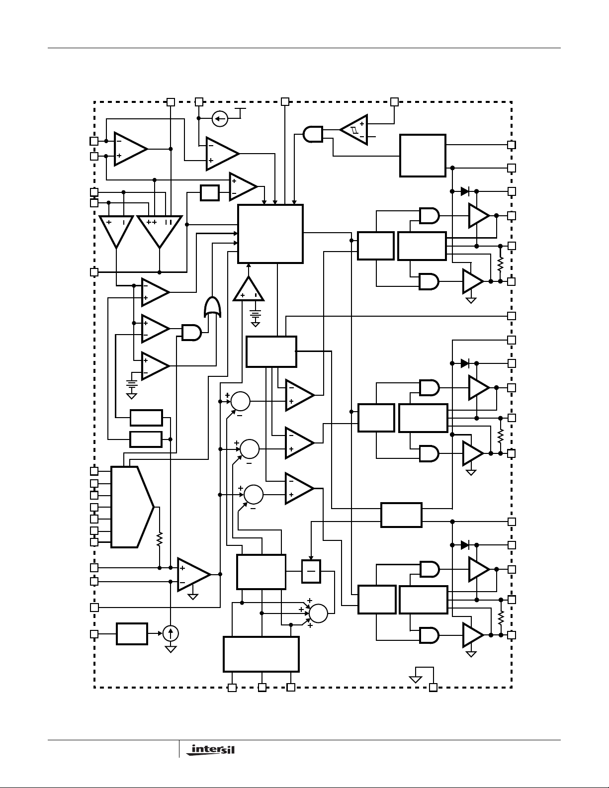
Block Diagram
ISL6566ISL6566
ISUM
IREF
RGND
VSEN
VDIFF
ISEN AMP
x1
UVP
OVP
OVP
ICOMP
x1
OCSET
+1V
100µA
OC
PGOOD
SOFT-START
AND
FAULT LOGIC
0.2V
CLOCK AND
SAWTOOTH
GENERATOR
0.66V
GATE
CONTROL
LOGIC
ENLL
POWER-ON
THROUGH
PROTECTION
RESET
SHOOT-
VCC
PVCC1
BOOT1
UGATE1
PHASE1
LGATE1
FS
PVCC2
BOOT2
VID4
VID3
VID2
VID1
VID0
VID12.5
VRM10
REF
FB
COMP
OFS
+150mV
x 0.82
DYNAMIC
VID
D/A
OFFSET
V
OVP
E/A
∑
∑
∑
CHANNEL
CURRENT
BALANCE
CHANNEL
CURRENT
SENSE
PWM1
PWM2
PWM3
UGATE2
GATE
CONTROL
LOGIC
1
N
GATE
CONTROL
∑
LOGIC
SHOOT-
THROUGH
PROTECTION
CHANNEL
DETECT
SHOOT-
THROUGH
PROTECTION
PHASE2
LGATE2
PVCC3
BOOT3
UGATE3
PHASE3
LGATE3
ISEN1
ISEN2
ISEN3
3
GND
FN9178.4
March 9, 2006
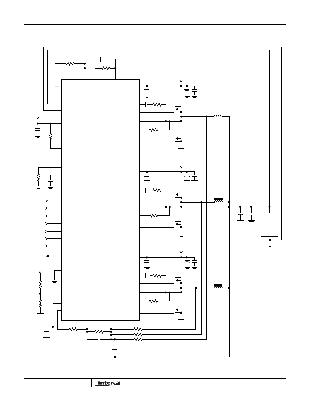
Typical Application - ISL6566
VDIFF
FB
COMP
ISL6566ISL6566
+12V
PVCC1
+5V
VSEN
RGND
VCC
OFS
FS
REF
VID4
VID3
VID2
VID1
VID0
VID12.5
VRM10
PGOOD
ISL6566
BOOT1
UGATE1
PHASE1
ISEN1
LGATE1
PVCC2
BOOT2
UGATE2
PHASE2
ISEN2
LGATE2
PVCC3
+12V
LOAD
+12V
+12V
GND
ENLL
IREF
OCSET
ICOMP
4
ISUM
BOOT3
UGATE3
PHASE3
ISEN3
LGATE3
FN9178.4
March 9, 2006
ISL6566ISL6566
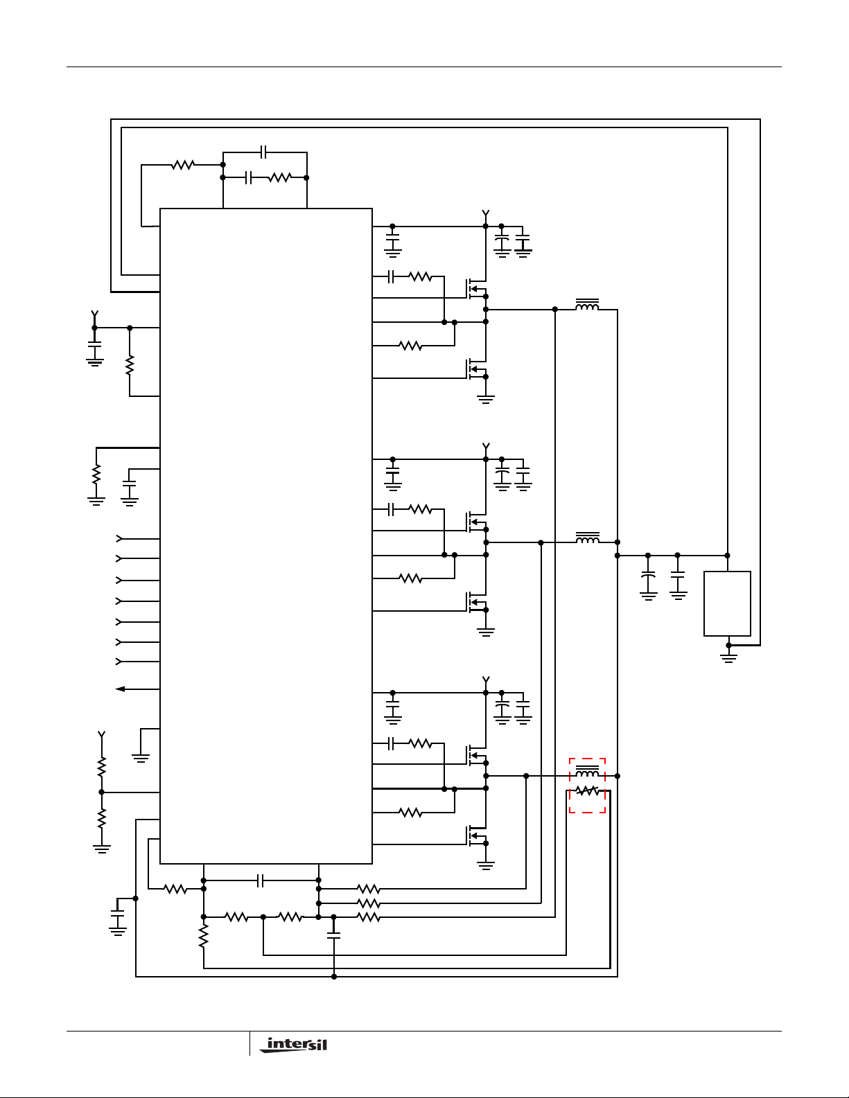
Typical Application - ISL6566 with NTC Thermal Compensation
+12V
VDIFF
FB
COMP
PVCC1
+5V
VSEN
RGND
VCC
OFS
FS
REF
VID4
VID3
VID2
VID1
VID0
VID12.5
VRM10
PGOOD
ISL6566
BOOT1
UGATE1
PHASE1
ISEN1
LGATE1
PVCC2
BOOT2
UGATE2
PHASE2
ISEN2
LGATE2
PVCC3
+12V
LOAD
+12V
+12V
GND
ENLL
IREF
OCSET
ICOMP
BOOT3
UGATE3
PHASE3
ISEN3
LGATE3
ISUM
5
PLACE IN CLOSE
PROXIMITY
NTC
FN9178.4
March 9, 2006

ISL6566ISL6566
Absolute Maximum Ratings
Supply Voltage, VCC . . . . . . . . . . . . . . . . . . . . . . . . . . . -0.3V to +6V
Supply Voltage, PVCC. . . . . . . . . . . . . . . . . . . . . . . . . -0.3V to +15V
Absolute Boot Voltage, V
Phase Voltage, V
GND - 8V (<400ns, 20µJ) to 24V (<200ns, V
PHASE
Upper Gate Voltage, V
V
- 3.5V (<100ns Pulse Width, 2µJ) to V
Lower Gate Voltage, V
PHASE
GND - 5V (<100ns Pulse Width, 2µJ) to PVCC+ 0.3V
. . . . . . . . GND - 0.3V to GND + 36V
BOOT
. . . . . . . . GND - 0.3V to 15V (PVCC = 12)
. . . . V
UGATE
LGATE
PHASE
. . . . . . . . GND - 0.3V to PVCC + 0.3V
BOOT-PHASE
- 0.3V to V
BOOT
BOOT
+ 0.3V
+ 0.3V
= 12V)
Thermal Information
Thermal Resistance θJA (°C/W) θJC (°C/W)
QFN Package (Notes 1, 2). . . . . . . . . . 32 3.5
Maximum Junction Temperature . . . . . . . . . . . . . . . . . . . . . . . 150°C
Maximum Storage Temperature Range. . . . . . . . . . . -65°C to 150°C
Maximum Lead Temperature (Soldering 10s) . . . . . . . . . . . . . 300°C
Input, Output, or I/O Voltage . . . . . . . . . GND - 0.3V to VCC + 0.3V
ESD Classification . . . . . . . . . . . . . . . . . . . . . . . Class I JEDEC STD
Recommended Operating Conditions
VCC Supply Voltage . . . . . . . . . . . . . . . . . . . . . . . . . . . . . +5V ±5%
PVCC Supply Voltage . . . . . . . . . . . . . . . . . . . . . . . +5V to 12V ±5%
Ambient Temperature (ISL6566CR, ISL6566CRZ) . . . . 0°C to 70°C
Ambient Temperature (ISL6566IR, ISL6566IRZ) . . . . . -40°C to 85°C
CAUTION: Stress above those listed in “Absolute Maximum Ratings” may cause permanent damage to the device. This is a stress only rating and operation of the
device at these or any other conditions above those indicated in the operational section of this specification is not implied.
NOTES:
is measured in free air with the component mounted on a high effective thermal conductivity test board with “direct attach” features. See
1. θ
JA
Tech Brief TB379.
2. For θ
, the “case temp” location is the center of the exposed metal pad on the package underside.
JC
Electrical Specifications Recommended Operating Conditions, Unless Otherwise Specified.
PARAMETER TEST CONDITIONS MIN TYP MAX UNITS
BIAS SUPPLY AND INTERNAL OSCILLATOR
Input Bias Supply Current I
Gate Drive Bias Current I
VCC POR (Power-On Reset) Threshold VCC Rising 4.25 4.38 4.50 V
PVCC POR (Power-On Reset) Threshold PVCC Rising 4.25 4.38 4.50 V
Oscillator Ramp Amplitude (Note 3) V
Maximum Duty Cycle (Note 3) - 66.6 - %
Oscillator Frequency, F
SW
CONTROL THRESHOLDS
ENLL Rising Threshold -0.66-V
ENLL Hysteresis - 100 - mV
COMP Shutdown Threshold COMP Falling 0.2 0.3 0.4 V
REFERENCE AND DAC
System Accuracy (VID = 1.0V - 1.850V) -0.5 - 0.5 %
System Accuracy (VID = 0.8V - 1.0V) -0.8 - 0.8 %
DAC Input Low Voltage (VR9, VR10) --0.4V
DAC Input High Voltage (VR9, VR10) 0.8 - - V
DAC Input Low Voltage (AMD) --0.6V
DAC Input High Voltage (AMD) 1.0 - - V
OFS Sink Current Accuracy (Negative Offset) R
OFS Source Current Accuracy (Positive Offset) R
; ENLL = high - 15 20 mA
VCC
; ENLL = high - 0.8 - mA
PVCC
VCC Falling 3.75 3.88 4.00 V
PVCC Falling 3.60 3.88 4.00 V
PP
-1.50-V
RT = 100kΩ (± 0.1%) 225 250 275 kHz
= 30kΩ from OFS to VCC 47.5 50.0 52.5 µA
OFS
= 10kΩ from OFS to GND 47.5 50.0 52.5 µA
OFS
6
FN9178.4
March 9, 2006

ISL6566ISL6566
Electrical Specifications Recommended Operating Conditions, Unless Otherwise Specified. (Continued)
PARAMETER TEST CONDITIONS MIN TYP MAX UNITS
ERROR AMPLIFIER
DC Gain (Note 3) R
Gain-Bandwidth Product (Note 3) C
Slew Rate (Note 3) C
Maximum Output Voltage Load = 1mA 3.90 4.20 - V
Minimum Output Voltage Load = -1mA - 0.85 1.0 V
OVERCURRENT PROTECTION
OCSET trip current 93 100 107 µA
OCSET Accuracy OCSET and ISUM Difference -5 0 5 mV
ICOMP Offset -5 0 5 mV
PROTECTION
Undervoltage Threshold VSEN falling 80 82 84 %VID
Undervoltage Hysteresis VSEN Rising - 3 - %VID
Overvoltage Threshold while IC Disabled V
Overvoltage Threshold VSEN Rising VID +
Overvoltage Hysteresis VSEN Falling - 50 - mV
Open Sense-Line Protection Threshold IREF Rising and Falling VDIFF
SWITCHING TIME (Note 3)
UGATE Rise Time t
LGATE Rise Time t
UGATE Fall Time t
LGATE Fall Time t
UGATE Turn-On Non-overlap t
LGATE Turn-On Non-overlap t
GATE DRIVE RESISTANCE (Note 3)
Upper Drive Source Resistance V
Upper Drive Sink Resistance V
Lower Drive Source Resistance V
Lower Drive Sink Resistance V
OVER TEMPERATURE SHUTDOWN
Thermal Shutdown Setpoint (Note 3) - 160 - °C
Thermal Recovery Setpoint (Note 3) - 100 - °C
NOTE:
3. Parameter magnitude guaranteed by design. Not 100% tested.
= 10K to ground - 96 - dB
L
= 100pF, RL = 10K to ground - 20 - MHz
L
= 100pF, Load = ±400µA-8-V/µs
L
, VRM9.0 Configuration 1.92 1.97 2.02 V
OVP
, Hammer and VRM10.0 Configurations 1.62 1.67 1.72 V
V
OVP
125mV
VID +
150mV
VID +
175mV
VDIFF + 1VVDIFF
+ 0.9V
RUGATE; VPVCC
RLGATE; VPVCC
FUGATE; VPVCC
FLGATE; VPVCC
PDHUGATE
PDHLGATE
= 12V, 15mA Source Current 1.25 2.0 3.0 Ω
PVCC
= 12V, 15mA Sink Current 0.9 1.65 3.0 Ω
PVCC
= 12V, 15mA Source Current 0.85 1.25 2.2 Ω
PVCC
= 12V, 15mA Sink Current 0.60 0.80 1.35 Ω
PVCC
= 12V, 3nF Load, 10% to 90% - 26 - ns
= 12V, 3nF Load, 10% to 90% - 18 - ns
= 12V, 3nF Load, 90% to 10% - 18 - ns
= 12V, 3nF Load, 90% to 10% - 12 - ns
; V
; V
= 12V, 3nF Load, Adaptive - 10 - ns
PVCC
= 12V, 3nF Load, Adaptive - 10 - ns
PVCC
+ 1.1V
V
V
7
FN9178.4
March 9, 2006
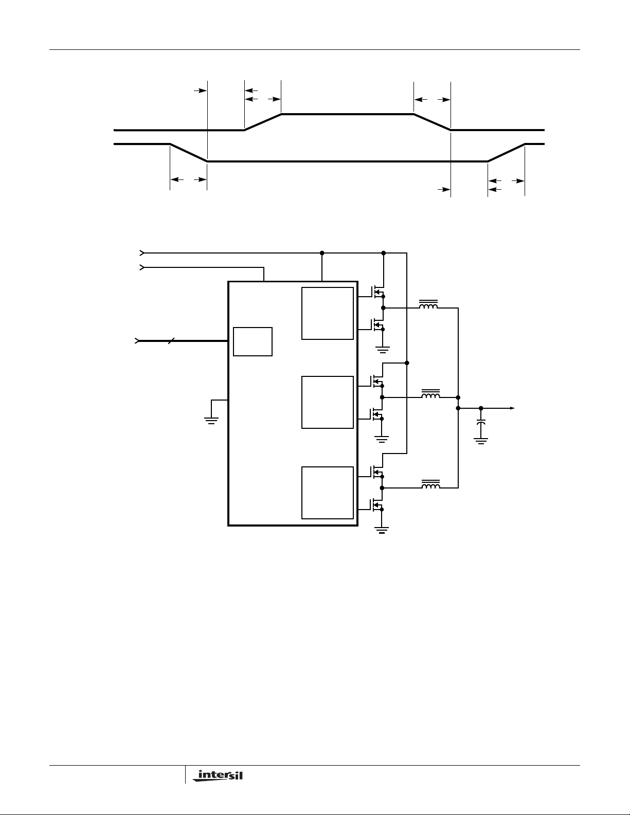
Timing Diagram
UGATE
LGATE
t
PDHUGATE
t
RUGATE
ISL6566ISL6566
t
FUGATE
t
FLGATE
Simplified Power System Diagram
+12V
IN
+5V
IN
VID
5-6
DAC
ISL6566
CHANNEL1
CHANNEL2
t
PDHLGATE
Q1
Q2
Q3
Q4
t
RLGATE
V
OUT
Functional Pin Description
VCC
VCC is the bias supply for the ICs small-signal circuitry.
Connect this pin to a +5V supply and locally decouple using
a quality 1.0µF ceramic capacitor.
PVCC1, PVCC2, PVCC3
These pins are the power supply pins for the corresponding
channel MOSFET drive, and can be connected to any
voltage from +5V to +12V, depending on the desired
MOSFET gate drive level.
The number of active channels is determined by the state of
PVCC2 and PVCC3. Leave PVCC3 unconnected or
grounded for 2-phase operation. For 1-phase operation
leave both PVCC3 and PVCC2 unconnected or grounded.
Q5
CHANNEL3
Q6
GND
GND is the bias and reference ground for the IC.
ENLL
This pin is a threshold-sensitive (approximately 0.66V) enable
input for the controller. Held low, this pin disables controller
operation. Pulled high, the pin enables the controller for
operation. ENLL has a internal 1.0µA pull-up to 5V.
FS
A resistor, placed from FS to ground, will set the switching
frequency. Refer to Equation 34 for proper resistor
calculation.
8
FN9178.4
March 9, 2006

ISL6566ISL6566
VID4, VID3, VID2, VID1, VID0, and VID12.5
These are the inputs for the internal DAC that provides the
reference voltage for output regulation. These pins respond to
TTL logic thresholds. The ISL6566 decodes the VID inputs to
establish the output voltage; see VID Tables for
correspondence between DAC codes and output voltage
settings. These pins are internally pulled high, to
approximately 1.2V, by 40µA (typically) internal current
sources; the internal pull-up current decreases to 0 as the VID
voltage approaches the internal pull-up voltage. All VID pins
are compatible with external pull-up voltages not exceeding
the IC’s bias voltage (VCC).
VRM10
This pin selects VRM10.0 DAC compliance when pulled high or
open. If VRM10 is grounded, VID12.5 selects the compliance
standard for the internal DAC: pulled to ground, it encodes the
DAC with AMD Hammer VID codes, while left open or pulled
high, it encodes the DAC with Intel VRM9.0 codes.
VSEN and RGND
VSEN and RGND are inputs to the precision differential
remote-sense amplifier and should be connected to the sense
pins of the remote load.
ICOMP, ISUM, and IREF
ISUM, IREF, and ICOMP are the DCR current sense
amplifier’s negative input, positive input, and output
respectively. For accurate DCR current sensing, connect a
resistor from each channel’s phase node to ISUM and
connect IREF to the summing point of the output inductors,
roughly Vout. A parallel R-C feedback circuit connected
between ISUM and ICOMP will then create a voltage from
IREF to ICOMP proportional to the voltage drop across the
inductor DCR. This voltage is referred to as the droop voltage
and is added to the differential remote-sense amplifier output.
Note: An optional 0.01µF ceramic capacitor can be placed
from the IREF pin to the ISUM pin, or from the IREF pin to
GND to help reduce any noise affects that may occur due to
layout.
VDIFF
VDIFF is the output of the differential remote-sense amplifier.
The voltage on this pin is equal to the difference between
VSEN and RGND added to the difference between IREF and
ICOMP. VDIFF therefore represents the output voltage plus
the droop voltage.
FB and COMP
These pins are the internal error amplifier inverting input and
output respectively. FB, VDIFF, and COMP are tied together
through external R-C networks to compensate the regulator.
REF
The REF input pin is the positive input of the error amplifier. It
is internally connected to the DAC output through a 1kΩ
resistor. A capacitor is used between the REF pin and ground
to smooth the voltage transition during Dynamic VID
operations.
OFS
The OFS pin provides a means to program a dc current for
generating an offset voltage across the resistor between FB
and VDIFF. The offset current is generated via an external
resistor and precision internal voltage references. The polarity
of the offset is selected by connecting the resistor to GND or
VCC. For no offset, the OFS pin should be left unconnected.
OCSET
This is the overcurrent set pin. Placing a resistor from OCSET
to ICOMP allows a 100µA current to flow out this pin,
producing a voltage reference. Internal circuitry compares the
voltage at OCSET to the voltage at ISUM, and if ISUM ever
exceeds OCSET, the overcurrent protection activates.
ISEN1, ISEN2 and ISEN3
These pins are used for balancing the channel currents by
sensing the current through each channel’s lower MOSFET
when it is conducting. Connect a resistor between the
ISEN1, ISEN2, and ISEN3 pins and their respective phase
node. This resistor sets a current proportional to the current
in the lower MOSFET during its conduction interval.
UGATE1, UGATE2, an d U G AT E3
Connect these pins to the corresponding upper MOSFET
gates. These pins are used to control the upper MOSFETs
and are monitored for shoot-through prevention purposes.
Maximum individual channel duty cycle is limited to 66%.
BOOT1, BOOT2, and BOOT3
These pins provide the bias voltage for the corresponding
upper MOSFET drives. Connect these pins to appropriatelychosen external bootstrap capacitors. Internal bootstrap
diodes connected to the PVCC pins provide the necessary
bootstrap charge.
PHASE1, PHASE2, and PHASE3
Connect these pins to the sources of the corresponding
upper MOSFETs. These pins are the return path for the
upper MOSFET drives.
LGATE1, LGATE2, and LGATE3
These pins are used to control the lower MOSFETs. Connect
these pins to the corresponding lower MOSFETs’ gates.
PGOOD
During normal operation PGOOD indicates whether the
output voltage is within specified overvoltage and
undervoltage limits. If the output voltage exceeds these limits
or a reset event occurs (such as an overcurrent event),
PGOOD is pulled low. PGOOD is always low prior to the end
of soft-start.
9
FN9178.4
March 9, 2006
 Loading...