®
ISL6566A
Data Sheet
Three-Phase Buck PWM Controller with
Two Integrated MOSFET Drivers and One
External Driver Signal
The ISL6566A three-phase PWM control IC provides a
precision voltage regulation system for advanced
microprocessors. The integration of power MOSFET drivers
into the controller IC marks a departure from the separate
PWM controller and driver configuration of previous multiphase product families. By reducing the number of external
parts, this integration is optimized for a cost and space
saving power management solution.
Outstanding features of this controller IC include programmable
VID codes compatible with Intel VRM9, VRM10, as well as
AMD Hammer microprocessors. A unity gain, differential
amplifier is provided for remote voltage sensing, compensating
for any potential difference between remote and local grounds.
The output voltage can also be positively or negatively offset
through the use of a single external resistor.
A unique feature of the ISL6566A is the combined use of
both DCR and r
current sensing. Load line voltage
DS(ON)
positioning (droop) and overcurrent protection are
accomplished through continuous inductor DCR current
sensing, while r
current sensing is used for accurate
DS(ON)
channel-current balance. Using both methods of current
sampling utilizes the best advantages of each technique.
Protection features of this controller IC include a set of
sophisticated overvoltage, undervoltage, and overcurrent
protection. Overvoltage results in the converter turning the
lower MOSFETs ON to clamp the rising output voltage and
protect the microprocessor. The overcurrent protection level is
set through a single external resistor. Furthermore, the
ISL6566A includes protection against an open circuit on the
remote sensing inputs. Combined, these features provide
advanced protection for the microprocessor and power system.
Ordering Information
TEMP.
PART NUMBER*
ISL6566ACR 0 to 70 40 Ld 6x6 QFN L40.6x6
ISL6566ACRZ (Note) 0 to 70 40 Ld 6x6 QFN (Pb-free) L40.6x6
ISL6566ACRZA (Note) 0 to 70 40 Ld 6x6 QFN (Pb-free) L40.6x6
ISL6566AIR -40 to 85 40 Ld 6x6 QFN L40.6x6
ISL6566AIRZ (Note) -40 to 85 40 Ld 6x6 QFN (Pb-free) L40.6x6
ISL6566AIRZA (Note) -40 to 85 40 Ld 6x6 QFN (Pb-free) L40.6x6
NOTE: Intersil Pb-free plus anneal products employ special Pb-free
material sets; molding compounds/die attach materials and 100%
matte tin plate termination finish, which are RoHS compliant and
compatible with both SnPb and Pb-free soldering operations. Intersil
Pb-free products are MSL classified at Pb-free peak reflow
temperatures that meet or exceed the Pb-free requirements of
IPC/JEDEC J STD-020
*Add “-T” suffix for tape and reel.
(°C) PACKAGE
PKG.
DWG. #
July 27, 2005
FN9200.2
Features
• Integrated Multi-Phase Power Conversion
- 1 or 2-Phase Operation with Internal Drivers
- 3-Phase Operation with External PWM Driver Signal
• Precision Core Voltage Regulation
- Differential Remote Voltage Sensing
- ±0.5% System Accuracy Over Temperature
- Adjustable Reference-Voltage Offset
• Precision Channel Current Sharing
- Uses Loss-Less r
DS(ON)
Current Sampling
• Accurate Load Line Programming
- Uses Loss-Less Inductor DCR Current Sampling
• Variable Gate Drive Bias: 5V to 12V
• Microprocessor Voltage Identification Inputs
- Up to a 6-Bit DAC
- Selectable between Intel’s VRM9, VRM10, or AMD
Hammer DAC codes
- Dynamic VID-on-the-fly Technology
• Multi-tiered Overvoltage and Overcurrent Protection
• Digital Soft-Start
• Selectable Operation Frequency up to 1.5MHz Per Phase
• Pb-Free Plus Anneal Available (RoHS Compliant)
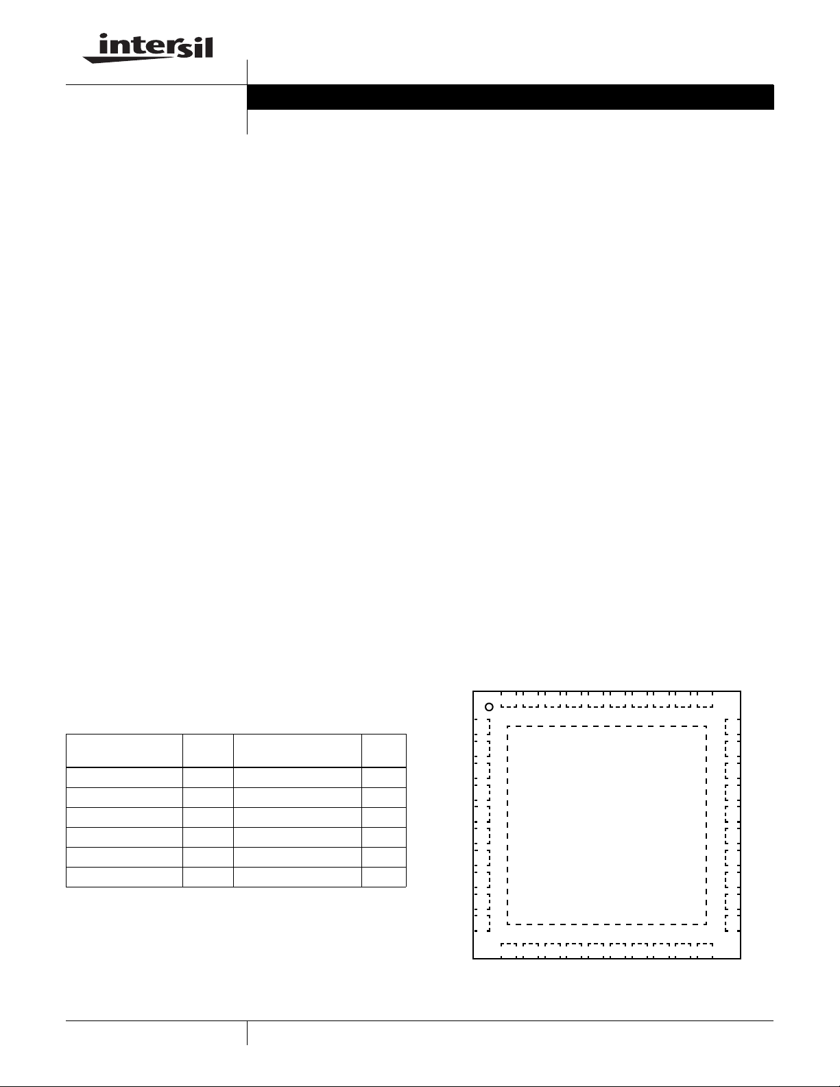
Pinout
ISL6566A (QFN)
TOP VIEW
VID3
VID4
VID1
VID0
VID12.5
VRM10
REF
OFS
VCC
COMP
FB
VDIFF
VID2
40
39 38 37 36 35 34 33 32 31
1
2
3
4
5
6
7
8
9
10
11 12 13 14 15 16 17 18 19 20
VSEN
RGND
ENLL
ICOMP
OCSET
FS
41
GND
ISUM
PGOOD
IREF
LGATE1
LGATE2
PVCC1
PVCC2
ISEN1
UGATE1
30
29
28
27
26
25
24
23
22
21
ISEN2
UGATE2
BOOT1
PHASE1
NC
PWM3
NC
ISEN3
EN_PH3
NC
PHASE2
BOOT2
1
CAUTION: These devices are sensitive to electrostatic discharge; follow proper IC Handling Procedures.
1-888-INTERSIL or1-888-468-3774
| Intersil (and design) is a registered trademark of Intersil Americas Inc.
All other trademarks mentioned are the property of their respective owners.
Copyright Intersil Americas Inc. 2005. All Rights Reserved
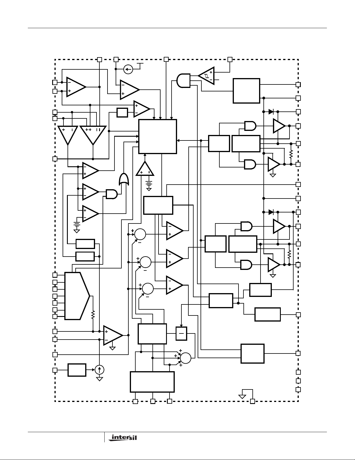
Block Diagram
ISL6566AISL6566A
ISUM
IREF
RGND
VSEN
VDIFF
ISEN AMP
x1
UVP
OVP
OVP
ICOMP
x1
OCSET
+1V
100µA
OC
PGOOD
SOFT-START
AND
FAULT LOGIC
0.2V
CLOCK AND
SAWTOOTH
GENERATOR
0.66V
GATE
CONTROL
LOGIC
ENLL
POWER-ON
THROUGH
PROTECTION
RESET
SHOOT-
VCC
PVCC1
BOOT1
UGATE1
PHASE1
LGATE1
FS
PVCC2
BOOT2
VID4
VID3
VID2
VID1
VID0
VID12.5
VRM10
REF
FB
COMP
OFS
+150mV
x 0.82
DYNAMIC
VID
D/A
OFFSET
V
OVP
E/A
∑
∑
∑
CHANNEL
CURRENT
BALANCE
CHANNEL
CURRENT
SENSE
PWM1
PWM2
PWM3
UGATE2
GATE
CONTROL
LOGIC
CHANNEL
DETECT
1
N
∑
SHOOT-
THROUGH
PROTECTION
PWM3
SIGNAL
LOGIC
PH2
DETECT
PH3 POR /
DETECT
PHASE2
LGATE2
EN_PH3
PWM3
NC
NC
NC
ISEN1
ISEN2
ISEN3
2
GND
FN9200.2
July 27, 2005
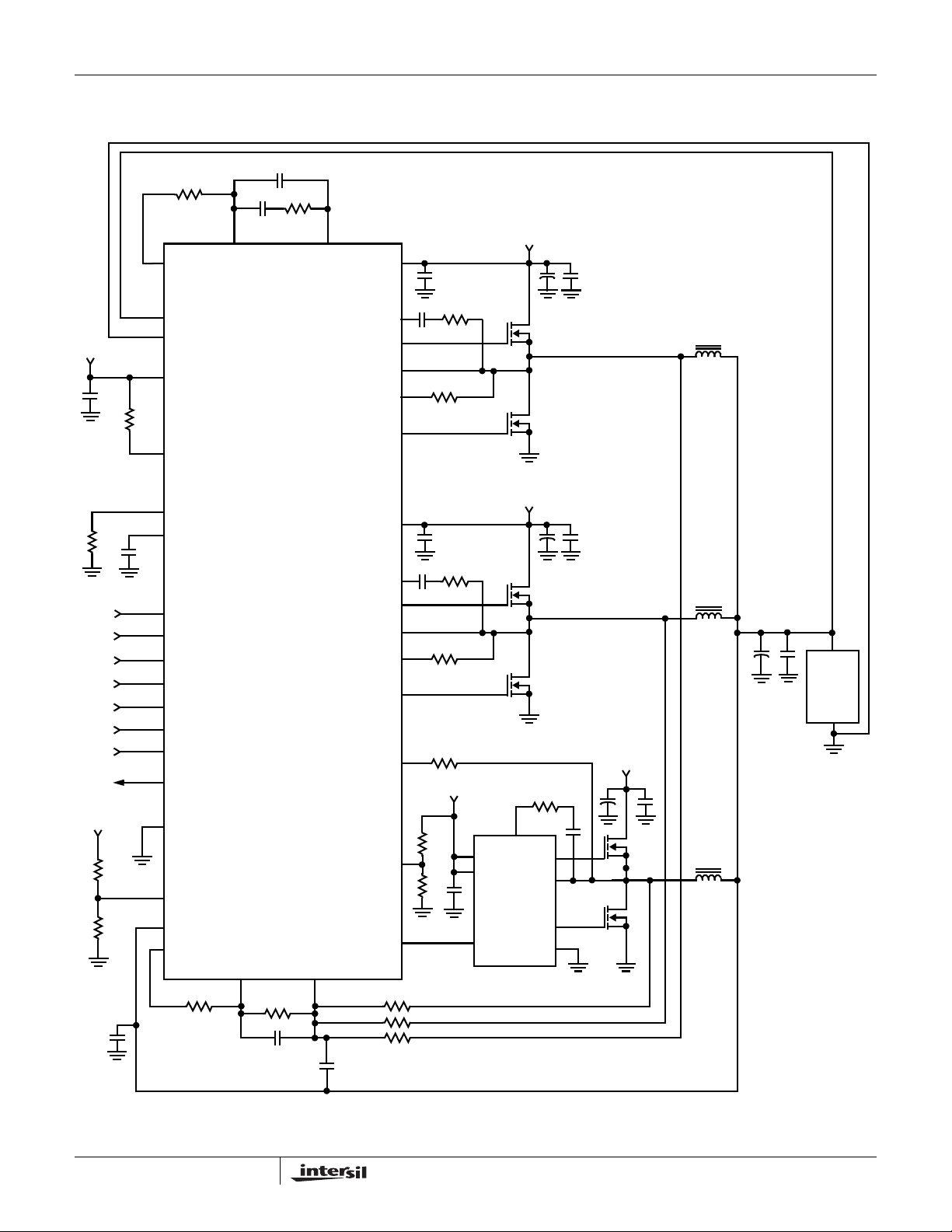
Typical Application - ISL6566A
VDIFF
FB
COMP
ISL6566AISL6566A
+12V
PVCC1
+5V
VSEN
RGND
VCC
OFS
FS
REF
VID4
VID3
VID2
VID1
VID0
VID12.5
VRM10
PGOOD
ISL6566A
BOOT1
UGATE1
PHASE1
ISEN1
LGATE1
PVCC2
BOOT2
UGATE2
PHASE2
ISEN2
LGATE2
ISEN3
+12V
LOAD
+12V
+12V
+12V
GND
ENLL
IREF
OCSET
ICOMP
BOOT
VCC
EN_PH3
PVCC
UGATE
PHASE
ISL6612
LGATE
PWM3
ISUM
3
PWM
GND
FN9200.2
July 27, 2005
ISL6566AISL6566A
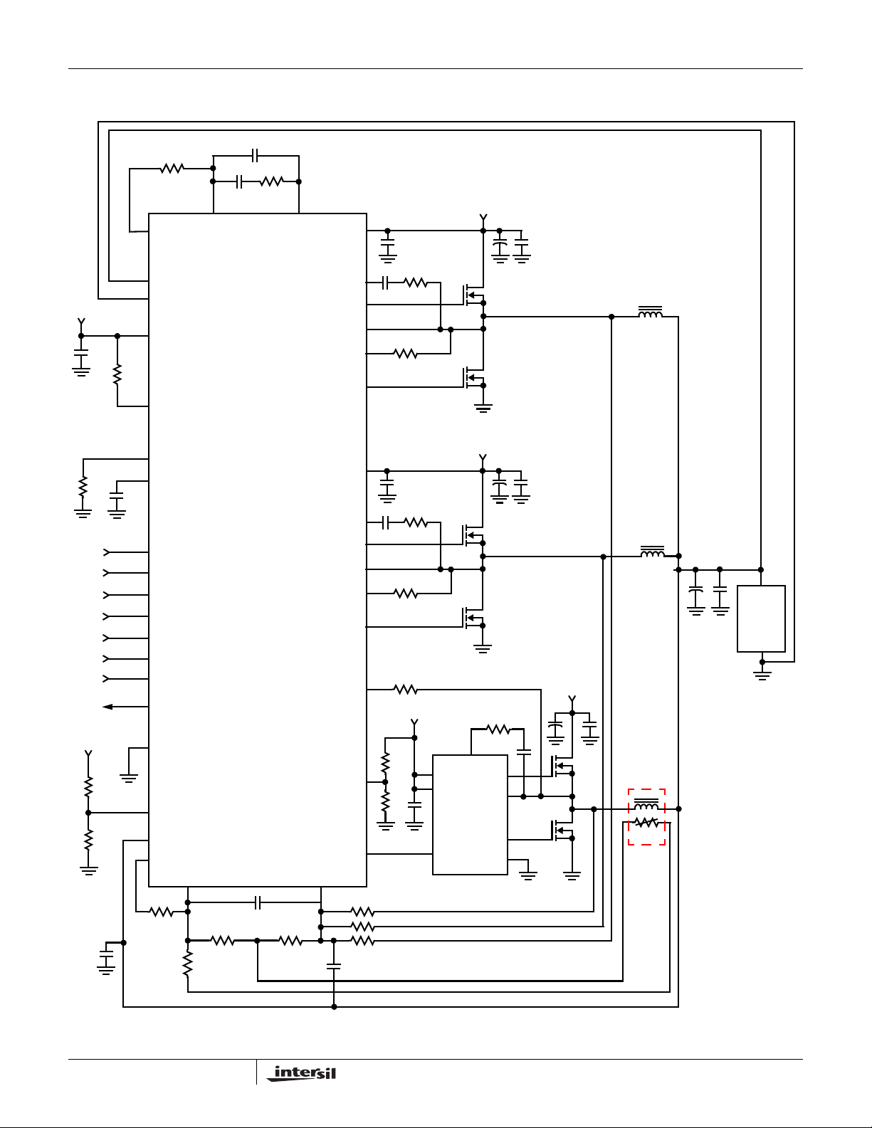
Typical Application - ISL6566A with NTC Thermal Compensation
+12V
VDIFF
FB
COMP
PVCC1
+5V
VSEN
RGND
VCC
OFS
FS
REF
VID4
VID3
VID2
VID1
VID0
VID12.5
VRM10
PGOOD
ISL6566A
BOOT1
UGATE1
PHASE1
ISEN1
LGATE1
PVCC2
BOOT2
UGATE2
PHASE2
ISEN2
LGATE2
ISEN3
+12V
LOAD
+12V
+12V
+12V
GND
ENLL
IREF
OCSET
ICOMP
PLACE
IN CLOSE
PROXIMITY
EN_PH3
VCC
PVCC
BOOT
UGATE
PHASE
ISL6612
LGATE
PWM3
ISUM
PWM
GND
4
NTC
FN9200.2
July 27, 2005

ISL6566AISL6566A
Absolute Maximum Ratings
Supply Voltage, VCC . . . . . . . . . . . . . . . . . . . . . . . . . . . -0.3V to +6V
Supply Voltage, PVCC. . . . . . . . . . . . . . . . . . . . . . . . . -0.3V to +15V
Absolute Boot Voltage, V
Phase Voltage, V
GND - 8V (<400ns, 20µJ) to 24V (<200ns, V
PHASE
Upper Gate Voltage, V
V
- 3.5V (<100ns Pulse Width, 2µJ) to V
Lower Gate Voltage, V
PHASE
GND - 5V (<100ns Pulse Width, 2µJ) to PVCC+ 0.3V
. . . . . . . . GND - 0.3V to GND + 36V
BOOT
. . . . . . . . GND - 0.3V to 15V (PVCC = 12)
. . . . V
UGATE
LGATE
PHASE
. . . . . . . . GND - 0.3V to PVCC + 0.3V
BOOT-PHASE
- 0.3V to V
BOOT
BOOT
+ 0.3V
+ 0.3V
= 12V)
Thermal Information
Thermal Resistance θJA (°C/W) θJC (°C/W)
QFN Package (Notes 1, 2). . . . . . . . . . 32 3.5
Maximum Junction Temperature . . . . . . . . . . . . . . . . . . . . . . . 150°C
Maximum Storage Temperature Range. . . . . . . . . . . -65°C to 150°C
Maximum Lead Temperature (Soldering 10s) . . . . . . . . . . . . . 300°C
Input, Output, or I/O Voltage . . . . . . . . . GND - 0.3V to VCC + 0.3V
ESD Classification . . . . . . . . . . . . . . . . . . . . . . . Class I JEDEC STD
Recommended Operating Conditions
VCC Supply Voltage . . . . . . . . . . . . . . . . . . . . . . . . . . . . . +5V ±5%
PVCC Supply Voltage . . . . . . . . . . . . . . . . . . . . . . . +5V to 12V ±5%
Ambient Temperature (ISL6566ACR, ISL6566ACRZ) . . 0°C to 70°C
Ambient Temperature (ISL6566AIR, ISL6566AIRZ) . .-40°C to 85°C
CAUTION: Stress above those listed in “Absolute Maximum Ratings” may cause permanent damage to the device. This is a stress only rating and operation of the
device at these or any other conditions above those indicated in the operational section of this specification is not implied.
NOTES:
is measured in free air with the component mounted on a high effective thermal conductivity test board with “direct attach” features. See
1. θ
JA
Tech Brief TB379.
2. For θ
, the “case temp” location is the center of the exposed metal pad on the package underside.
JC
Electrical Specifications Recommended Operating Conditions, Unless Otherwise Specified.
PARAMETER TEST CONDITIONS MIN TYP MAX UNITS
BIAS SUPPLY AND INTERNAL OSCILLATOR
Input Bias Supply Current I
Gate Drive Bias Current I
VCC POR (Power-On Reset) Threshold VCC Rising 4.25 4.38 4.50 V
PVCC POR (Power-On Reset) Threshold PVCC Rising 4.25 4.38 4.50 V
Oscillator Ramp Amplitude (Note 3) V
Maximum Duty Cycle (Note 3) - 66.6 - %
Oscillator Frequency, F
SW
CONTROL THRESHOLDS
ENLL Rising Threshold -0.66-V
ENLL Hysteresis - 100 - mV
EN_PH3 Rising Threshold 1.190 1.220 1.250 V
EN_PH3 Falling Threshold 1.000 1.045 1.090 V
COMP Shutdown Threshold COMP Falling 0.2 0.3 0.4 V
REFERENCE AND DAC
System Accuracy (VID = 1.0V - 1.850V) -0.5 - 0.5 %
System Accuracy (VID = 0.8V - 1.0V) -0.8 - 0.8 %
DAC Input Low Voltage (VR9, VR10) --0.4V
DAC Input High Voltage (VR9, VR10) 0.8 - - V
DAC Input Low Voltage (AMD) --0.6V
; ENLL = high - 15 20 mA
VCC
; ENLL = high - 1.06 - mA
PVCC
VCC Falling 3.75 3.88 4.00 V
PVCC Falling 3.60 3.88 4.00 V
PP
-1.50-V
RT = 100kΩ (± 0.1%) 225 250 275 kHz
5
FN9200.2
July 27, 2005

ISL6566AISL6566A
Electrical Specifications Recommended Operating Conditions, Unless Otherwise Specified. (Continued)
PARAMETER TEST CONDITIONS MIN TYP MAX UNITS
DAC Input High Voltage (AMD) 1.0 - - V
OFS Sink Current Accuracy (Negative Offset) R
OFS Source Current Accuracy (Positive Offset) R
ERROR AMPLIFIER
DC Gain (Note 3) R
Gain-Bandwidth Product (Note 3) C
Slew Rate (Note 3) CL = 100pF, Load = ±400µA-8-V/µs
Maximum Output Voltage Load = 1mA 3.90 4.20 - V
Minimum Output Voltage Load = -1mA - 0.85 1.0 V
OVERCURRENT PROTECTION
OCSET trip current 93 100 107 µA
OCSET Accuracy OCSET and ISUM Difference -5 0 5 mV
ICOMP Offset -5 0 5 mV
PROTECTION
Undervoltage Threshold VSEN falling 80 82 84 %VID
Undervoltage Hysteresis VSEN Rising - 3 - %VID
Overvoltage Threshold while IC Disabled V
Overvoltage Threshold VSEN Rising VID +
Overvoltage Hysteresis VSEN Falling - 50 - mV
Open Sense-Line Protection Threshold IREF Rising and Falling VDIFF
SWITCHING TIME (Note 3)
UGATE Rise Time t
LGATE Rise Time t
UGATE Fall Time t
LGATE Fall Time t
UGATE Turn-On Non-overlap t
LGATE Turn-On Non-overlap t
GATE DRIVE RESISTANCE (Note 3)
Upper Drive Source Resistance V
Upper Drive Sink Resistance V
Lower Drive Source Resistance V
Lower Drive Sink Resistance V
OVER TEMPERATURE SHUTDOWN
Thermal Shutdown Setpoint (Note 3) - 160 - °C
Thermal Recovery Setpoint (Note 3) - 100 - °C
NOTE:
3. Parameter magnitude guaranteed by design. Not 100% tested.
= 30kΩ from OFS to VCC 47.5 50.0 52.5 µA
OFS
= 10kΩ from OFS to GND 47.5 50.0 52.5 µA
OFS
= 10K to ground - 96 - dB
L
= 100pF, RL = 10K to ground - 20 - MHz
L
, VRM9.0 Configuration 1.92 1.97 2.02 V
OVP
V
, Hammer and VRM10.0 Configurations 1.62 1.67 1.72 V
OVP
125mV
VID +
150mV
VID +
175mV
VDIFF + 1VVDIFF
+ 0.9V
RUGATE; VPVCC
RLGATE; VPVCC
FUGATE; VPVCC
FLGATE; VPVCC
PDHUGATE
PDHLGATE
= 12V, 15mA Source Current 1.25 2.0 3.0 Ω
PVCC
= 12V, 15mA Sink Current 0.9 1.65 3.0 Ω
PVCC
= 12V, 15mA Source Current 0.85 1.25 2.2 Ω
PVCC
= 12V, 15mA Sink Current 0.60 0.80 1.35 Ω
PVCC
= 12V, 3nF Load, 10% to 90% - 26 - ns
= 12V, 3nF Load, 10% to 90% - 18 - ns
= 12V, 3nF Load, 90% to 10% - 18 - ns
= 12V, 3nF Load, 90% to 10% - 12 - ns
; V
= 12V, 3nF Load, Adaptive - 10 - ns
PVCC
; V
= 12V, 3nF Load, Adaptive - 10 - ns
PVCC
+ 1.1V
V
V
6
FN9200.2
July 27, 2005
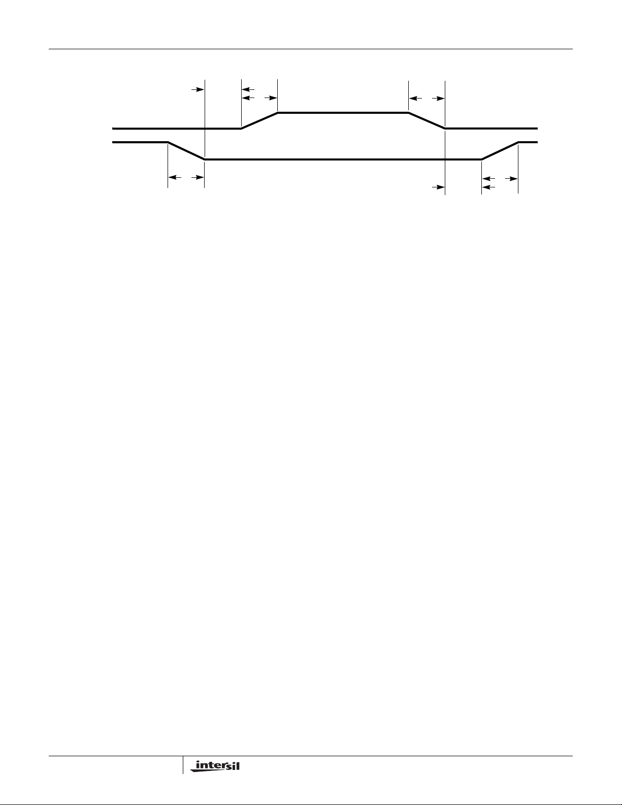
Timing Diagram
UGATE
LGATE
t
PDHUGATE
t
RUGATE
ISL6566AISL6566A
t
FUGATE
t
FLGATE
Simplified Power System Diagram
Functional Pin Description
VCC
VCC is the bias supply for the ICs small-signal circuitry.
Connect this pin to a +5V supply and locally decouple using
a quality 1.0µF ceramic capacitor.
PVCC1 and PVCC2
These pins are the power supply pins for the corresponding
channel MOSFET drive, and can be connected to any
voltage from +5V to +12V, depending on the desired
MOSFET gate drive level.
Internally these pins are bonded so DO NOT connect
these pins to different voltages.
GND
GND is the bias and reference ground for the IC.
ENLL
This pin is a threshold-sensitive (approximately 0.66V) enable
input for the controller. Held low, this pin disables controller
operation. Pulled high, the pin enables the controller for
operation. ENLL has a internal 1.0µA pull-up to 5V.
FS
A resistor, placed from FS to ground, will set the switching
frequency. Refer to Equation 34 for proper resistor
calculation.
VID4, VID3, VID2, VID1, VID0, and VID12.5
These are the inputs for the internal DAC that provides the
reference voltage for output regulation. These pins respond to
TTL logic thresholds. The ISL6566A decodes the VID inputs
to establish the output voltage; see VID Tables for
correspondence between DAC codes and output voltage
settings. These pins are internally pulled high, to
approximately 1.2V, by 40µA (typically) internal current
sources; the internal pull-up current decreases to 0 as the VID
voltage approaches the internal pull-up voltage. All VID pins
are compatible with external pull-up voltages not exceeding
the IC’s bias voltage (VCC).
t
RLGATE
t
PDHLGATE
VRM10
This pin selects VRM10.0 DAC compliance when pulled high or
open. If VRM10 is grounded, VID12.5 selects the compliance
standard for the internal DAC: pulled to ground, it encodes the
DAC with AMD Hammer VID codes, while left open or pulled
high, it encodes the DAC with Intel VRM9.0 codes.
VSEN and RGND
VSEN and RGND are inputs to the precision differential
remote-sense amplifier and should be connected to the sense
pins of the remote load.
ICOMP, ISUM, and IREF
ISUM, IREF, and ICOMP are the DCR current sense
amplifier’s negative input, positive input, and output
respectively. For accurate DCR current sensing, connect a
resistor from each channel’s phase node to ISUM and
connect IREF to the summing point of the output inductors,
roughly Vout. A parallel R-C feedback circuit connected
between ISUM and ICOMP will then create a voltage from
IREF to ICOMP proportional to the voltage drop across the
inductor DCR. This voltage is referred to as the droop voltage
and is added to the differential remote-sense amplifier output.
Note: An optional 0.01µF ceramic capacitor can be placed
from the IREF pin to the ISUM pin to help reduce any noise
affects that may occur due to layout.
VDIFF
VDIFF is the output of the differential remote-sense amplifier.
The voltage on this pin is equal to the difference between
VSEN and RGND added to the difference between IREF and
ICOMP. VDIFF therefore represents the output voltage plus
the droop voltage.
FB and COMP
These pins are the internal error amplifier inverting input and
output respectively. FB, VDIFF, and COMP are tied together
through external R-C networks to compensate the regulator.
REF
The REF input pin is the positive input of the error amplifier. It
is internally connected to the DAC output through a 1kΩ
resistor. A capacitor is used between the REF pin and ground
7
FN9200.2
July 27, 2005
ISL6566AISL6566A
to smooth the voltage transition during Dynamic VID
operations.
OFS
The OFS pin provides a means to program a dc current for
generating an offset voltage across the resistor between FB
and VDIFF. The offset current is generated via an external
resistor and precision internal voltage references. The polarity
of the offset is selected by connecting the resistor to GND or
VCC. For no offset, the OFS pin should be left unconnected.
OCSET
This is the overcurrent set pin. Placing a resistor from OCSET
to ICOMP allows a 100µA current to flow out this pin,
producing a voltage reference. Internal circuitry compares the
voltage at OCSET to the voltage at ISUM, and if ISUM ever
exceeds OCSET, the overcurrent protection activates.
ISEN1, ISEN2 and ISEN3
These pins are used for balancing the channel currents by
sensing the current through each channel’s lower MOSFET
when it is conducting. Connect a resistor between the
ISEN1, ISEN2, and ISEN3 pins and their respective phase
node. This resistor sets a current proportional to the current
in the lower MOSFET during its conduction interval.
UGATE1 and UGATE2
Connect these pins to the corresponding upper MOSFET
gates. These pins are used to control the upper MOSFETs
and are monitored for shoot-through prevention purposes.
Maximum individual channel duty cycle is limited to 66%.
BOOT1 and BOOT2
These pins provide the bias voltage for the corresponding
upper MOSFET drives. Connect these pins to appropriatelychosen external bootstrap capacitors. Internal bootstrap
diodes connected to the PVCC pins provide the necessary
bootstrap charge.
PHASE1 and PHASE2
Connect these pins to the sources of the upper MOSFETs.
These pins are the return path for the upper MOSFET
drives.
LGATE1 and LGATE2
These pins are used to control the lower MOSFETs. Connect
these pins to the corresponding lower MOSFETs’ gates.
PWM3
Pulse-width modulation output. Connect this pin to the PWM
input pin of an Intersil driver IC if 3-phase operation is
desired.
EN_PH3
This pin has two functions. First, a resistor divider connected
to this pin will provide a POR power up synch between the
on-chip and external driver. The resistor divider should be
designed so that when the POR-trip point of the external
driver is reached the voltage on this pin should be 1.220V.
The second function of this pin is disabling PWM3 for 2phase operation. This can be accomplished by connecting
this pin to a +5V supply.
PGOOD
During normal operation PGOOD indicates whether the
output voltage is within specified overvoltage and
undervoltage limits. If the output voltage exceeds these limits
or a reset event occurs (such as an overcurrent event),
PGOOD is pulled low. PGOOD is always low prior to the end
of soft-start.
Operation
Multi-Phase Power Conversion
Microprocessor load current profiles have changed to the
point that the advantages of multi-phase power conversion
are impossible to ignore. The technical challenges
associated with producing a single-phase converter that is
both cost-effective and thermally viable have forced a
change to the cost-saving approach of multi-phase. The
ISL6566A controller helps simplify implementation by
integrating vital functions and requiring minimal external
components. The block diagram on page 2 provides a top
level view of multi-phase power conversion using the
ISL6566A controller.
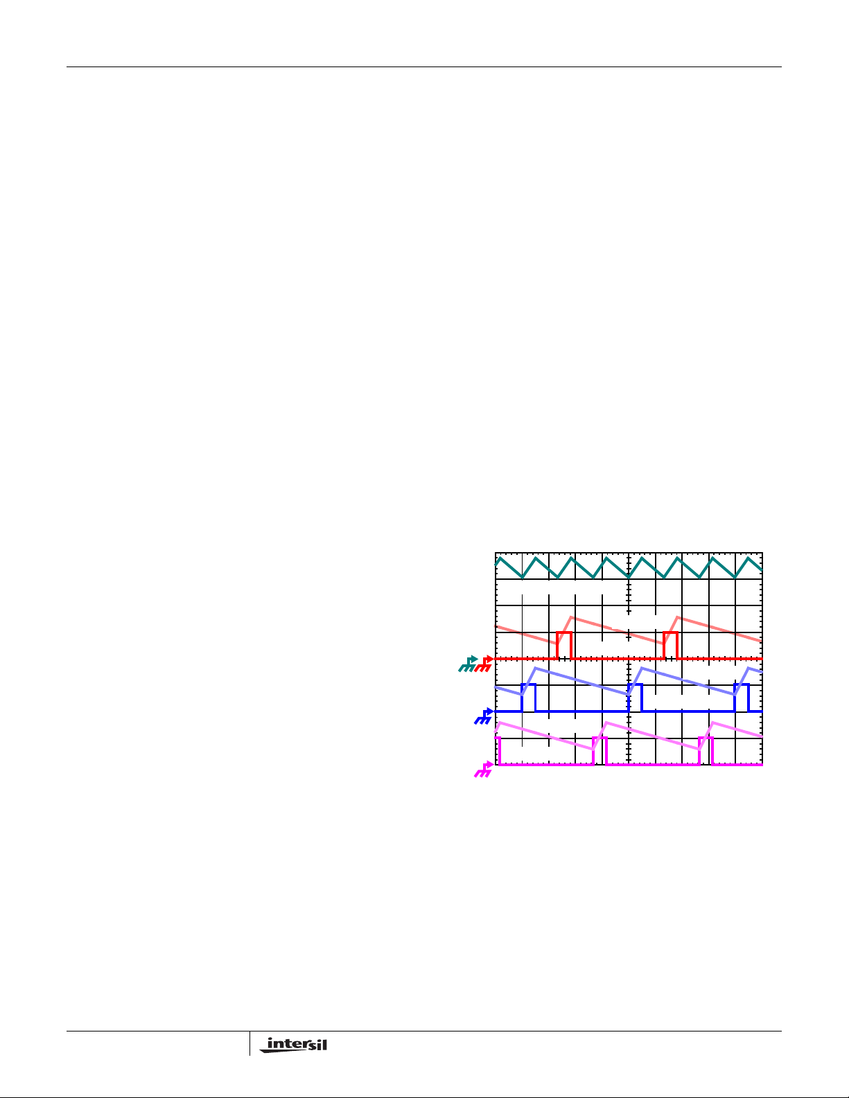
IL1 + IL2 + IL3, 7A/DIV
IL3, 7A/DIV
PWM3, 5V/DIV
IL2, 7A/DIV
PWM2, 5V/DIV
IL1, 7A/DIV
PWM1, 5V/DIV
1µs/DIV
FIGURE 1. PWM AND INDUCTOR-CURRENT WAVEFORMS
FOR 3-PHASE CONVERTER
Interleaving
The switching of each channel in a multi-phase converter is
timed to be symmetrically out of phase with each of the other
channels. In a 3-phase converter, each channel switches 1/3
cycle after the previous channel and 1/3 cycle before the
following channel. As a result, the three-phase converter has
a combined ripple frequency three times greater than the
ripple frequency of any one phase. In addition, the peak-topeak amplitude of the combined inductor currents is reduced
in proportion to the number of phases (Equations 1 and 2).
8
FN9200.2
July 27, 2005
ISL6566AISL6566A
Increased ripple frequency and lower ripple amplitude mean
that the designer can use less per-channel inductance and
lower total output capacitance for any performance
specification.
Figure 1 illustrates the multiplicative effect on output ripple
frequency. The three channel currents (IL1, IL2, and IL3)
combine to form the AC ripple current and the DC load
current. The ripple component has three times the ripple
frequency of each individual channel current. Each PWM
pulse is terminated 1/3 of a cycle after the PWM pulse of the
previous phase. The peak-to-peak current for each phase is
about 7A, and the dc components of the inductor currents
combine to feed the load.
To understand the reduction of ripple current amplitude in the
multi-phase circuit, examine the equation representing an
individual channel peak-to-peak inductor current.
VINV
–()V
OUT
I
------------------------------------------------------=
PP
LfSV
In Equation 1, V
IN
and V
IN
OUT
are the input and output
OUT
(EQ. 1)
voltages respectively, L is the single-channel inductor value,
and f
is the switching frequency.
S
The output capacitors conduct the ripple component of the
inductor current. In the case of multi-phase converters, the
capacitor current is the sum of the ripple currents from each
of the individual channels. Compare Equation 1 to the
expression for the peak-to-peak current after the summation
of N symmetrically phase-shifted inductor currents in
Equation 2. Peak-to-peak ripple current decreases by an
amount proportional to the number of channels. Outputvoltage ripple is a function of capacitance, capacitor
equivalent series resistance (ESR), and inductor ripple
current. Reducing the inductor ripple current allows the
designer to use fewer or less costly output capacitors.
VINNV
–()V
OUT
I
------------------------------------------------------------=
CPP,
LfSV
OUT
IN
(EQ. 2)
Another benefit of interleaving is to reduce input ripple
current. Input capacitance is determined in part by the
maximum input ripple current. Multi-phase topologies can
improve overall system cost and size by lowering input ripple
current and allowing the designer to reduce the cost of input
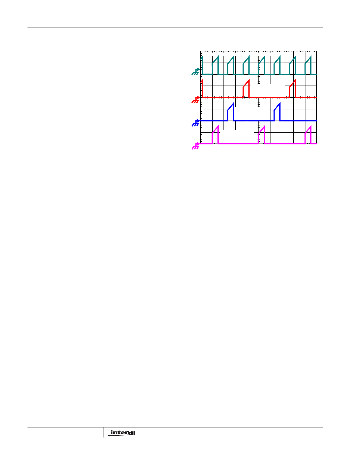
capacitance. The example in Figure 2 illustrates input
currents from a three-phase converter combining to reduce
the total input ripple current.
The converter depicted in Figure 2 delivers 1.5V to a 36A load
from a 12V input. The RMS input capacitor current is 5.9A.
Compare this to a single-phase converter also stepping down
12V to 1.5V at 36A. The single-phase converter has 11.9A
RMS input capacitor current. The single-phase converter
must use an input capacitor bank with twice the RMS current
capacity as the equivalent three-phase converter.
INPUT-CAPACITOR CURRENT, 10A/DIV
CHANNEL 3
INPUT CURRENT
10A/DIV
CHANNEL 2
INPUT CURRENT
10A/DIV
CHANNEL 1
INPUT CURRENT
10A/DIV
1µs/DIV
FIGURE 2. CHANNEL INPUT CURRENTS AND INPUT-
CAPACITOR RMS CURRENT FOR 3-PHASE
CONVERTER
Figures 22 and 23 in the section entitled Input Capacitor
Selection can be used to determine the input-capacitor RMS
current based on load current, duty cycle, and the number of
channels. They are provided as aids in determining the
optimal input capacitor solution.
PWM Operation
The timing of each converter leg is set by the number of
active channels. The default channel setting for the
ISL6566A is three. One switching cycle is defined as the
time between the internal PWM1 pulse termination signals.
The pulse termination signal is the internally generated clock
signal that triggers the falling edge of PWM1. The cycle time
of the pulse termination signal is the inverse of the switching
frequency set by the resistor between the FS pin and
ground. Each cycle begins when the clock signal commands
PWM1 to go low. The PWM1 transition signals the internal
channel-1 MOSFET driver to turn off the channel-1 upper
MOSFET and turn on the channel-1 synchronous MOSFET.
In the default channel configuration, the PWM2 pulse
terminates 1/3 of a cycle after the PWM1 pulse. The PWM3
pulse terminates 1/3 of a cycle after PWM2.
If EN_PH3 is connected to a +5V source, two channel
operation is selected and the PWM2 pulse terminates 1/2 of
a cycle after the PWM1 pulse terminates. If the BOOT2 and
PHASE2 pins are both connected to +12V, single channel
operation is selected.
Once a PWM pulse transitions low, it is held low for a
minimum of 1/3 cycle. This forced off time is required to
ensure an accurate current sample. Current sensing is
described in the next section. After the forced off time
expires, the PWM output is enabled. The PWM output state
is driven by the position of the error amplifier output signal,
V
, minus the current correction signal relative to the
COMP
sawtooth ramp as illustrated in Figure 3. When the modified
9
FN9200.2
July 27, 2005
 Loading...