

Page 1
现货库存、技术资料、百科信息、热点资讯,精彩尽在鼎好!
TM
ISL6562
Data Sheet March 2001
Microprocessor CORE Voltage Regulator
Two-Phase Buck PWM Controller
The ISL6562 two-phase current mode, PWM control IC
together with companion gate drivers, the HIP6601A,
HIP6602A, HIP6603A or HIP6604 and MOSFETs provides a
precision voltage regulation system for advanced
microprocessors. Two-phase power conversion is a marked
departure from earlier single phase converter configurations
previously employed to satisfy the ever increasing current
demands of modern microprocessors. Multi-phase
converters, by distributing the power and load current results
in smaller and lower cost transistors with fewer input and
output capacitors. These reductions accrue from the higher
effective conversion frequency with higher frequency ripple
current due to the phase interleaving process of this
topology. For example, a two phase converter operating at
350kHz per phase will have a ripple frequency of 700kHz.
Moreover, greater converter bandwidth of this design results
in faster response to load transients.
Outstanding features of this controller IC include
programmable VID codes from the microprocessor that
range from 1.050V to 1.825V with an accuracy of ±0.8%.
Pull up currents on these VID pins eliminates the need for
external pull up resistors.
Another feature of this controller IC is the PWRGD monitor
circuit which is held low until the CORE voltage increases, to
within 18% of the programmed voltage. Over-voltage, 24%
above programmed CORE voltage, results in the PWRGD
output going low to indicate that the CORE is above the
specified limit. Under voltage is also detected and results in
PWRGD going low if the CORE voltage falls 18% below the
programmed level. Over-current protection folds back the
output voltage to 95mV, reducing the regulator dissipation.
These features provide monitoring and protection for the
microprocessor and power system.
Ordering Information
PART NUMBER TEMP. (oC) PACKAGE PKG. NO.
ISL6562CB 0 to 70 16 Ld SOIC M16.15
ISL6562CB-T 16 Ld SOIC Tape and Reel
ISL6560/62EVAL1 Evaluation Platform
File Number 9012
Features
• Two-Phase Power Conversion
• Precision Channel Current Sharing
• Precision CORE Voltage Regulation
- ±0.8% Accuracy
• Microprocessor Voltage Identification Input
- 5-Bit VID Input
- 1.050V to 1.825V in 25mV Steps
- Programmable “Droop” Voltage
• Fast Transient Recovery Time
• Over Current Protection
• High Ripple Frequency, (Channel Frequency
Times Number of Channels). . . . . . . . . . . . .100kHz to 2MHz
Applications
• VRM8.5 Modules
• Intel® Tualatin Processor Voltage Regulator
• Low Output Voltage, High Current DC/DC Converters
Related Literature
• Technical Brief TB363 “Guidelines for Handling and
Processing Moisture Sensitive Surface Mount Devices
(SMDs)”
Pinout
ISL6562 (SOIC)
TOP VIEW
1
VID3
2
VID2
3
VID1
VID0
4
VID25mV
5
COMP CS+
6
FB
7
CT
8
16
15
14
13
12
11
10
9
VCC
REF
CSPWM1
PWM2
PWRGD
GND
1
Intel® is a registered trademark of Intel Corporation. | Copyright © Intersil Americas Inc. 2001, All Rights Reserved
CAUTION: These devices are sensitive to electrostatic discharge; follow proper IC Handling Procedures.
1-888-INTERSIL or 321-724-7143 | Intersil and Design is a trademark of Intersil Americas Inc.
Page 2
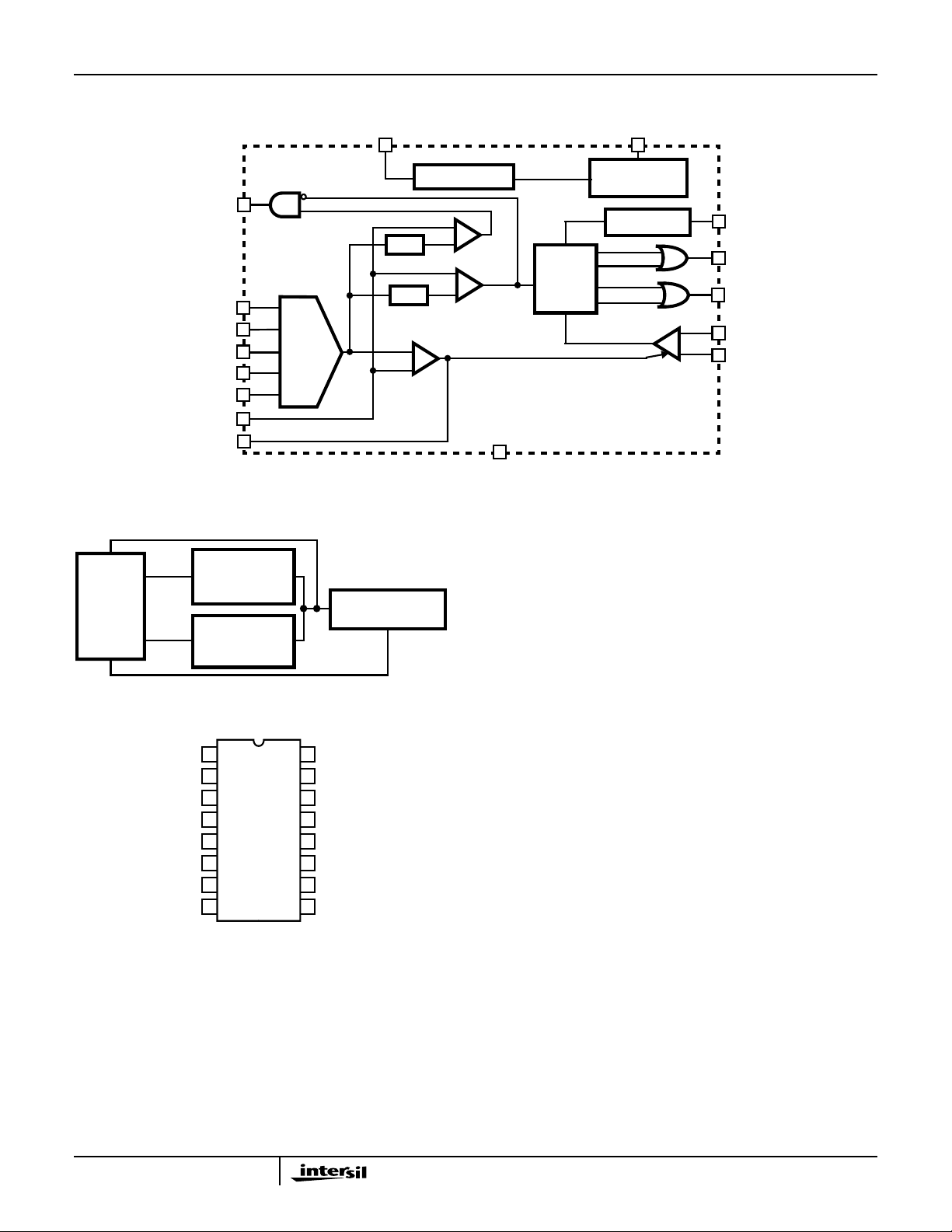
Block Diagram
REF
ISL6562
VCC
PWRGD
VID3
VID2
VID1
VID0
VID25mV
FB
COMP
D/A
Simplified Power System Diagram
FB
PWM 1
ISL6562
PWM 2
VID
SYNCHRONOUS
RECTIFIED BUCK
CHANNEL
MICROPROCESSOR
SYNCHRONOUS
RECTIFIED BUCK
CHANNEL
3V REFERENCE
X 0.82
X1.24
E/A
+
-
UVLO and
BIAS CIRCUITS
+
-
UV
+
-
OVP
GND
CONTROL
LOGIC
OSCILLATOR
CMP
+
-
CT
PWM1
PWM2
CS+
CS-
Current Sense Comparator. Pulling this pin to ground
disables the oscillator and drives both PWM outputs low.
FB (Pin 7)
Inverting input of the internal transconductance error
amplifier.
CT (Pin 8)
A capacitor on this terminal sets the frequency of the internal
oscillator.
Functional Pin Description
1
VID3
2
VID2
3
VID1
VID0
4
VID25mV
5
COMP CS+
6
FB
7
CT
8
VID3 (Pin 1), VID2 (Pin 2), VID1 (Pin 3), VID0 (Pin 4)
and VID25mV (Pin 5)
V oltage Identification inputs from microprocessor. These pins
respond to TTL and 3.3V logic signals. The ISL6562 decodes
VID bits to establish the output voltage. See Table 1.
COMP (Pin 6)
Output of the internal transconductance error amplifier.
Voltage at this terminal sets the output current level of the
16
15
14
13
12
11
10
9
VCC
REF
CSPWM1
PWM2
PWRGD
GND
GND (Pin 9)
Bias and referenceground. All signals are referenced to this
pin.
PWRGD (Pin 10)
Open drain connection. A high voltage level at this pin with a
resistor connected to this terminal and VCC indicates that
CORE voltage is at the proper level,
CS+ (Pin 11) and CS- (Pin 14) These inputs monitor the
supply current to the converter positive input voltage. CS+ is
connected directly to the decoupled supply voltage and
current sampling resistor. CS- is connected to the other end
of the current sampling resistor and the upper drains of the
series transistors.
PWM2 (Pin 12) and PWM1 (Pin 13)
PWM outputs connected to the gate driver ICs.
REF (Pin 15)
Three volt supply used to bias the output of the
transconductance amplifier.
VCC (Pin 16)
Bias supply. Connect this pin to a 12V supply.
2
Page 3

ISL6562
Absolute Maximum Ratings Thermal Information
Supply Voltage (VCC) . . . . . . . . . . . . . . . . . . . . . . . . . -0.3V to 15V
CS+. CS- . . . . . . . . . . . . . . . . . . . . . . . . . . . . . -0.3V to VCC + 0.3V
PWRGD. . . . . . . . . . . . . . . . . . . . . . . . . . . . . . . . . . . . -0.3V to VCC
All Other Inputs and Outputs . . . . . . . . . . . . . . . . . . . . . .-0.3V to 5V
ESD Rating
Human Body Model (Per MIL-STD-883 Method 3015.7). . . . TBD
Machine Model (Per EIAJ ED-4701 Method C-111). . . . . . . . TBD
Operating Conditions
Ambient Temperature Range. . . . . . . . . . . . . . . . . . . . .0oC to 70oC
Maximum Operating Junction Temperature. . . . . . . . . . . . . . 125oC
Supply Voltage, VCC . . . . . . . . . . . . . . . . . . . . . . . . . . . . 12V ±10%
CAUTION: Stresses above those listed in “Absolute Maximum Ratings” may cause permanent damage to the device. This is a stress only rating and operation of the
device at these or any other conditions above those indicated in the operational sections of this specification is not implied.
NOTE:
1. θJA is measured with the component mounted on a low effective thermal conductivity test board in free air. See Tech Brief TB379 for details.
Electrical Specifications Recommended Operating Conditions, Unless Otherwise Noted
PARAMETER SYMBOL TEST CONDITIONS MIN TYP MAX UNITS
VCC SUPPLY CURRENT
Input Supply Current I
Input Supply Current, UVLO Mode I
Undervoltage Lock Out Voltage V
CC
CC(UVLO)
UVLO
Undervoltage Lock Out Hysteresis 0.1 0.4 0.8 V
DAC and REFERENCE VOLTAGES
Minimum DAC Programed Voltage V
Middle DAC Programed Voltage V
Maximum DAC Programed Voltage V
FB
FB
FB
Line Regulation ∆V
Crowbar Trip Point at FB Input V
Crowbar Reset Point at FB Input V
Crowbar Response Time I
Reference Voltage V
Output Current I
CROWBAR
CROWBAR
CROWBAR
REF
REF
VID INPUTS
Input Low Voltage V
Input High Voltage V
VID Pull-Up I
IL(VID)
IH(VID)
VID
Internal Pull-Up Voltage 4.5 5.0 5.5 V
OSCILLATOR
Maximum Frequency f
Frequency Variation ∆f
CT Charging Current I
CT Charging Current I
CT(MAX)
CT
CT
CT
ERROR AMPLIFIER
Output Resistance R
Transconductance g
O(ERR)
m(ERR)
VCC = 12V - 5.8 9.0 mA
VCC ≤ V
DAC Programmed to 1.050V 1.042 1.050 1.058 V
DAC Programmed to 1.500V 1.488 1.500 1.512 V
DAC Programmed to 1.825V 1.811 1.825 1.839 V
VCC = 10V to 14V - 0.05 - %
FB
Percent of Nominal DAC Voltage 114 124 134 %
Percent of Nominal DAC Voltage 50 60 70 %
Overvoltage to PWM Going Low - 300 - ns
0mA ≤ I
REF
VIDx = 0V or VIDx = 3V 10 20 40 µA
TA = 25oC, CT = 91pF 430 500 570 kHz
TA = 25oC, VFB in Regulation 130 150 170 µA
TA = 25oC, VFB = 0V 26 36 46 µA
Thermal Resistance (Note 1) θJA (oC/W)
SOIC Package . . . . . . . . . . . . . . . . . . . . . . . . . . . . . 106
Maximum Junction Temperature (Plastic Package) . . . . . . . .150oC
Maximum Storage Temperature Range. . . . . . . . . . -65oC to 150oC
Maximum Lead Temperature (Soldering 10s) . . . . . . . . . . . . .300oC
(SOIC - Lead Tips Only)
, VCC Rising - 5.7 8.9 mA
UVLO
5.4 6.4 6.9 V
≤ 1mA 2.952 3.000 3.048 V
300 - - µA
- - 0.6 V
2.2 - - V
2.0 - - MHz
- 200 - kΩ
2.0 2.2 2.4 mS
3
Page 4

ISL6562
Electrical Specifications Recommended Operating Conditions, Unless Otherwise Noted
PARAMETER SYMBOL TEST CONDITIONS MIN TYP MAX UNITS
Output Current I
Input Bias Current I
Maximum Output Voltage
Output Disable Threshold
FB Low Foldback Threshold V
-3dB Bandwidth BW
O(ERR)
FB
V
COMP(MAX)
V
COMP(OFF)
FB(LOW)
ERR
CURRENT SENSE
Threshold Voltage V
Current Limit Foldback Voltage V
COMP
/∆V
CS
∆V
Input Bias Current I
Response Time t
CS(TH)
CS(FOLD)
n
, I
CS+
CS
POWER GOOD COMPARATOR
Undervoltage Threshold
Overvoltage Threshold
Output Voltage Low
V
PWRGD(UV)
V
PWRGD(OV)
V
OL(PWRGD)IPWRGD(SINK)
Response Time - 200 - ns
PWM OUTPUTS
Output Voltage Low V
Output Voltage High V
Output Current I
Duty Cycle Limit, by Design D
.
OL(PWM)IPWM(SINK)
OH(PWM)IPWM(SOURCE)
PWM
MAX
VOLTAGE IDENTIFICATION CODE AT
PROCESSOR PINS
0 01001.050
1 01001.075
0 00111.100
1 00111.125
0 00101.150
1 00101.175
0 00011.200
1 00011.225
0 00001.250
1 00001.275
0 11111.300
1 11111.325
0 11101.350
1 11101.375
0 11011.400
1 11011.425
FB Forced to V
- 3% - 1 - mA
OUT
- 5 100 nA
FB Forced to V
- 3% - 3.0 - V
OUT
560 720 800 mV
375 425 500 mV
COMP = Open - 500 - kHz
CS+ = VCC, FB Forced to V
- 3% 69 79 89 mV
OUT
0.8 ≤ COMP ≤ 1V - 0 15 mV
FB ≤ 375mV 37 47 58 mV
1 V ≤ V
i
CS+ = CS- = VCC - 0.5 5.0 µA
CS-
≤ 3V - 25 - V/V
COMP
CS+ - (CS-) ≥ 89mV to PWM Going Low - 50 - ns
Percent of Nominal Output 76 82 88 %
Percent of Nominal Output 114 124 134 %
= 100µA - 30 200 mV
= 400µA - 100 500 mV
= 400µA 4.5 5.0 5.5 V
0.4 1 - mA
Per Phase, Relative to f
CT
- - 50 %
VOLTAGE IDENTIFICATION CODE AT
VCCCORE
PROCESSOR PINS
(VDC)VID25mV VID3 VID2 VID1 VID0
0 11001.450
1 11001.475
0 10111.500
1 10111.525
0 10101.550
1 10101.575
0 10011.600
1 10011.625
0 10001.650
1 10001.675
0 01111.700
1 01111.725
0 01101.750
1 01101.775
0 01011.800
1 01011.825
VCCCORE
(VDC)VID25mV VID3 VID2 VID1 VID0
4
Page 5

Small Outline Plastic Packages (SOIC)
ISL6562
N
INDEX
AREA
123
-A-
E
-B-
SEATING PLANE
D
A
-C-
0.25(0.010) BM M
H
L
h x 45
o
α
e
B
0.25(0.010) C AM BS
M
NOTES:
1. Symbols are defined in the “MO Series Symbol List”inSection2.2of
Publication Number 95.
2. Dimensioning and tolerancing per ANSI Y14.5M-1982.
3. Dimension “D” doesnotincludemold flash, protrusions or gate burrs.
Mold flash, protrusion and gate burrs shall not exceed 0.15mm (0.006
inch) per side.
4. Dimension“E” doesnot includeinterlead flashor protrusions.Interlead
flash and protrusions shall not exceed 0.25mm (0.010 inch) per side.
5. The chamfer on thebodyisoptional.If it is not present, a visual index
feature must be located within the crosshatched area.
6. “L” is the length of terminal for soldering to a substrate.
7. “N” is the number of terminal positions.
8. Terminal numbers are shown for reference only.
9. Theleadwidth“B”,as measured0.36mm (0.014inch) orgreaterabove
the seating plane, shall not exceed a maximum value of 0.61mm
(0.024 inch).
10. Controllingdimension: MILLIMETER. Convertedinch dimensions are
not necessarily exact.
A1
C
0.10(0.004)
M16.15 (JEDEC MS-012-AC ISSUE C)
16 LEAD NARROW BODY SMALL OUTLINE PLASTIC
PACKAGE
INCHES MILLIMETERS
SYMBOL
A 0.0532 0.0688 1.35 1.75 -
A1 0.0040 0.0098 0.10 0.25 -
B 0.013 0.020 0.33 0.51 9
C 0.0075 0.0098 0.19 0.25 D 0.3859 0.3937 9.80 10.00 3
E 0.1497 0.1574 3.80 4.00 4
e 0.050 BSC 1.27 BSC H 0.2284 0.2440 5.80 6.20 h 0.0099 0.0196 0.25 0.50 5
L 0.016 0.050 0.40 1.27 6
N16 167
o
α
0
o
8
o
0
o
8
Rev. 0 12/93
NOTESMIN MAX MIN MAX
-
All Intersil products are manufactured, assembled and tested utilizing ISO9000 quality systems.
Intersil Corporation’s quality certifications can be viewed at website www.intersil.com/design/quality
Intersil products are sold by description only. Intersil Corporation reserves the right to make changes in circuit design and/or specifications at any time without notice.
Accordingly ,the reader is cautioned to verifythat data sheetsare current beforeplacing orders. Informationfurnished by Intersil is believed to be accurate andreliable. However ,no responsibility is assumed by Intersil or its subsidiaries for its use; nor for any infringements of patents or other rights of third parties which may result from its use.
No license is granted by implication or otherwise under any patent or patent rights of Intersil or its subsidiaries.
For information regarding Intersil Corporation and its products, see web site www.intersil.com
Sales Office Headquarters
NORTH AMERICA
Intersil Corporation
2401 Palm Bay Rd., Mail Stop 53-204
Palm Bay, FL 32905
TEL: (321) 724-7000
FAX: (321) 724-7240
5
EUROPE
Intersil SA
Mercure Center
100, Rue de la Fusee
1130 Brussels, Belgium
TEL: (32) 2.724.2111
FAX: (32) 2.724.22.05
ASIA
Intersil Ltd.
8F-2, 96, Sec. 1, Chien-kuo North,
Taipei, Taiwan 104
Republic of China
TEL: 886-2-2515-8508
FAX: 886-2-2515-8369
 Loading...