®
ISL6559
Data Sheet December 29, 2004
Multi-Phase PWM Controller
The ISL6559 provides core-voltage regulation by driving 2 to
4 interleaved synchronous-rectified buck-conv erter channels
in parallel. Interleaving the channel timing results in
increased ripple frequency which reduces input and output
ripple currents. The reduction in ripple results in lower
component cost, reduced dissipation, and a smaller
implementation area.
The ISL6559 uses cost and space-saving r
for channel current balance, active voltage positioning, and
over-current protection. Output voltage is monitored by an
internal differential remote sense amplifier. A high-bandwidth
error amplifier drives the output voltage to match the
programmed 5-bit DAC reference voltage. The resulting
compensation signal guides the creation of pulse width
modulated (PWM) signals to control companion Intersil
MOSFET drivers. The OFS pin allows direct offset of the
DAC voltage from 0V to 50mV using a single external
resistor. The entire system is trimmed to ensure a system
accuracy of ±
1% over temperature.
Outstanding features of this controller IC include
Dynamic VID
TM
technology allowing seamless on-the-fly VID
changing without the need of any external components.
Output voltage “droop” or active voltage positioning is
optional. When employed, it allows the reduction in size and
cost of the output capacitors required to support load
transients. A threshold-sensitive enable input allows the use
of an external resistor divider for start-up coordination with
Intersil MOSFET drivers or any other devices powered from
a separate supply.
Superior over-voltage protection is achiev ed by gating on the
lower MOSFET of all phases to crowbar the output voltage.
An optional second crowbar on V
, formed with an external
IN
MOSFET or SCR gated by the OVP pin, is triggered when
an over-voltage condition is detected. Under-voltage
conditions are detected, but PWM operation is not disrupted.
Over-current conditions cause a hiccup-mode response as
the controller repeatedly tries to restart. After a set number
of failed startup attempts, the controller latches off. A power
good logic signal indicates when the converter output is
between the UV and OV thresholds.
DS(ON)
sensing
FN9084.8
Features
• Multi-Phase Power Conversion
- 2, 3 or 4 Phase Operation
• Active Channel Current Balancing
• Precision r
Current Sharing
DS(ON)
- Lossless
-Low Cost
• Input Voltage: 12V or 5V Bias
• Precision CORE Voltage Regulation
-±
1% S y s t e m A c c u r a c y Over Temperature
- Differential Remote Output Voltage Sensing
- Programmable Reference Offset
• Microprocessor Voltage Identification Input
- 5-Bit VID Input
- 0.800V to 1.550V in 25mV Steps
- Dynamic VID Technology
• Programmable Droop Voltage
• Fast Transient Recovery Time
• Over Current Protection
• Digital Soft Start
• Threshold Sensitive Enable Input
• High Ripple Frequency (160kHz to 4MHz)
• QFN Package:
- Compliant to JEDEC PUB95 MO-220 QFN - Quad Flat
No Leads - Pac kage Outline
- Near Chip Scale Package f ootprint, which impro v es PC B
efficiency and has a thinner profile
• Pb-Free Available (RoHS Compliant)
Applications
• AMD Hammer F am ily Processor V ol t ag e Regu l a to r
• Low Output Vo ltage, High Current DC-DC Converters
• Voltage Regulator Modules
Pinouts
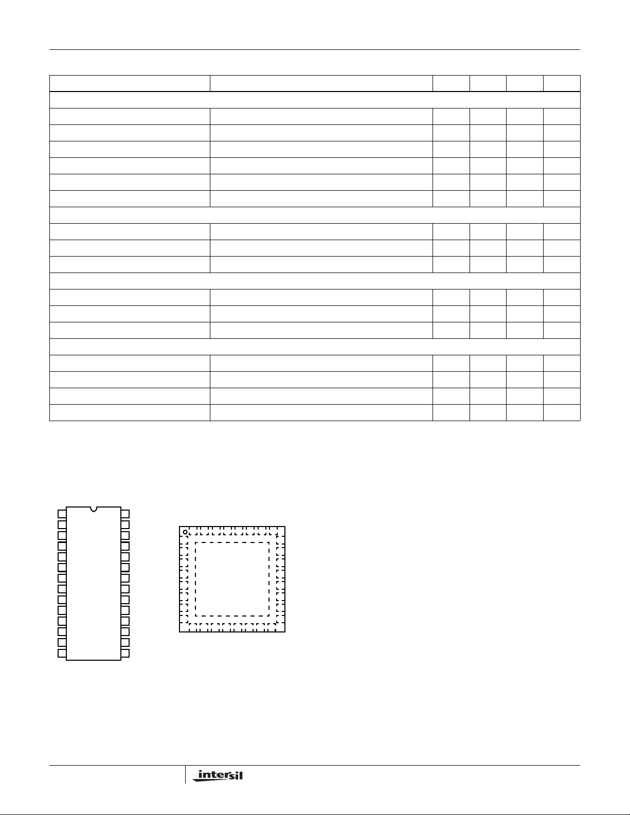
ISL6559CB (28 LEAD SOIC)
TOP VIEW TOP VIEW
28
27
26
25
24
23
22
21
20
19
18
17
16
15
EN
FS/DIS
PGOOD
PWM4
ISEN4
ISEN1
PWM1
PWM2
GND
ISEN2
ISEN3
PWM3
VCC
GND
GND
OVP
VID4
VID3
VID2
VID1
VID0
OFS
COMP
FB
IOUT
VDIFF
VSEN
RGND
1
2
3
4
5
6
7
8
9
10
11
12
13
14
ISL6559CR (32 LEAD QFN)
VID3NCVID4
32 31 30 29 28 27 26 25
VID2
1
VID1
2
VID0
3
NC
4
OFS
5
6
COMP
FB
7
NC
8
910111213141516
IOUT
VSEN
VDIFF
NC = NO CONNECT
OVP
GNDENFS/DIS
GND
RGND
GND
VCC
PGOOD
24
PWM4
23
ISEN4
22
ISEN1
21
PWM1
20
PWM2
19
GND
18
ISEN2
17
ISEN3
PWM3
1
Dynamic VID is a trademark of Intersil Americas Inc. All other trademarks mentioned are the property of their respective owners.
CAUTION: These devices are sensitive to electrostatic discharge; follow proper IC Handling Procedures.
1-888-INTERSIL or 321-724-7143
| Intersil (and design) is a registered trademark of Intersil Americas Inc.
Copyright © Intersil Americas Inc. 2002-2004. All Rights Reserved.
ISL6559
Ordering Information
PART # TEMP. (°C) PACKAGE PKG. DWG. #
ISL6559CB 0 to 70 28 Ld SOIC M28.3
ISL6559CBZ* 0 to 70 28 Ld SOIC (Pb-free) M28.3
ISL6559CB-T 28 Ld SOIC Tape and Reel
ISL6559CBZ-T* 28 Ld SOIC Tape and Reel (Pb-free)
ISL6559CR 0 to 70 32 Ld 5x5 QFN L32.5x5
ISL6559CRZ* 0 to 70 32 Ld 5x5 QFN (Pb-free) L32.5x5
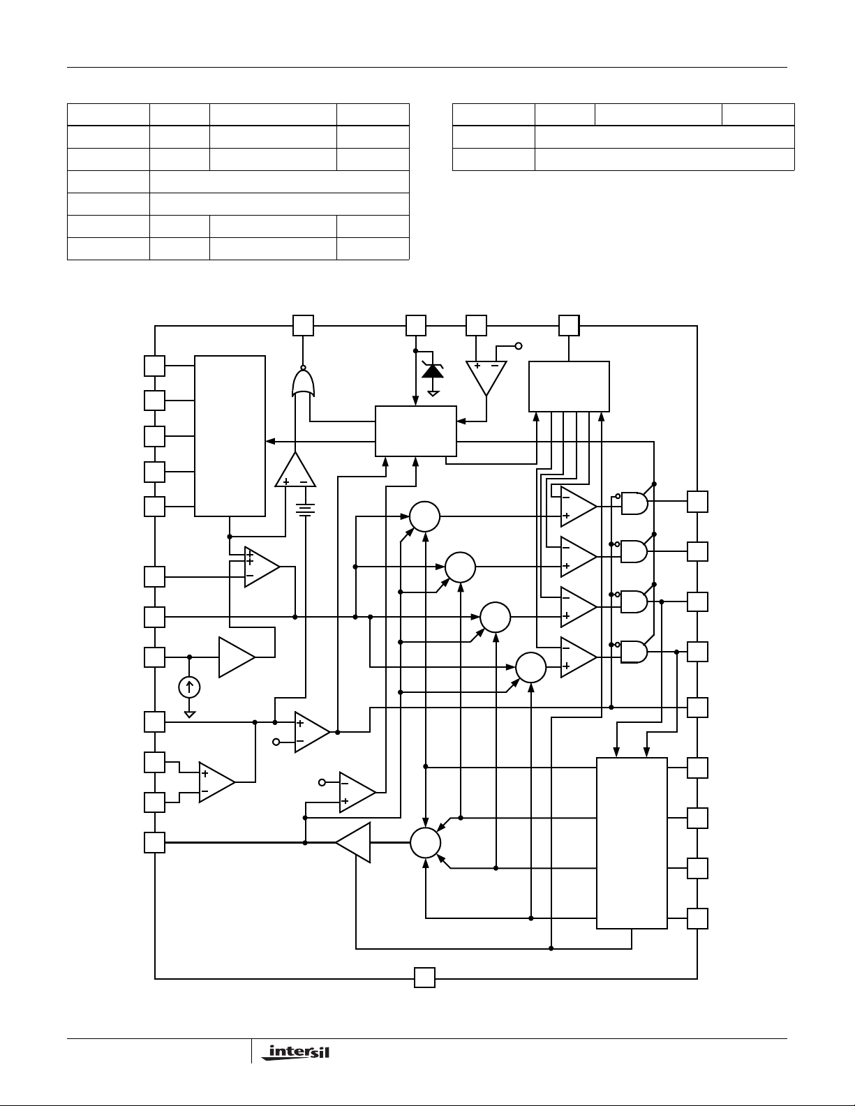
Block Diagram
PGOOD VCC
VID4
VID3
VID2
VID1
VID0
FB
COMP
OFS
DYNAMIC
VID
DAC
x 0.1
E/A
UV
-
+
350mV
POR
AND
SOFT START
+
+
+
Ordering Information (Continued)
PART # TEMP. (°C ) PACKAGE PKG. DW G. #
ISL6559CR-T 32 Ld 5x5 QFN Tape and Reel
ISL6559CRZ-T* 32 Ld 5x5 QFN Tape and Reel (Pb-free)
NOTE: * Intersil Pb-free products employ special Pb-free material sets;
molding compounds/die attach materials and 100% matte tin plate
termination finish, which are RoHS compliant and compatible with both
SnPb and Pb-free soldering operations. Intersil Pb-free products are
MSL classified at Pb-free peak reflow temperatures that meet or
exceed the Pb-free requirements of IPC/JEDEC J STD-020.
EN
1.23V
6V
-
+
+
-
+
+
FS/DIS
OSCILLATOR
AND
SAWTOOTH
PWM1
PWM2
PWM3
PWM4
VDIFF
VSEN
RGND
IOUT
100µA
DIFF
AVERAGE
2
2.2V
OV
90µA
OC
1/N
GND
-
+
OVP
I1
+
+
+
+
I2
I3
I4
N PHASES
CURRENT
SENSE
&
PHASE
DETECT
ISEN1
ISEN2
ISEN3
ISEN4
FN9084.8
December 29, 2004
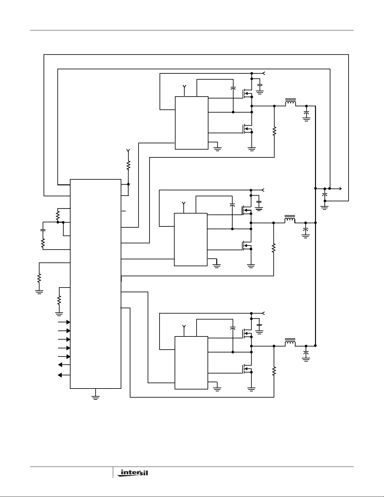
Typical Application - 3 Phase Converter
ISL6559
+12V
PVCC
+12V
BOOT
UGATE
VCC
DRIVER
HIP6601B
PWM
+12V
300Ω
ISL6559
VSEN
RGND
R
FB
C
C
R
C
R
OFS
R
T
VDIFF
FB
IOUT
COMP
OFS
FS/DIS
VID4
VID3
VID2
VID1
VID0
PGOOD
OVP
GND
VCC
PWM4
ISEN4
PWM1
ISEN1
PWM2
ISEN2
PWM3
ISEN3
NC
VCC
PWM
VCC
PWM
PVCC
PVCC
+12V
DRIVER
HIP6601B
+12V
DRIVER
HIP6601B
BOOT
BOOT
PHASE
LGATE
GND
UGATE
PHASE
LGATE
GND
UGATE
PHASE
LGATE
GND
+12V
+12V
R
R
R
ISEN1
ISEN2
ISEN3
V
OUT
3
FN9084.8
December 29, 2004
ISL6559
Absolute Maximum Ratings
Supply Voltage, VCC . . . . . . . . . . . . . . . . . . . . . . . . . . . . . . . . . +7V
Input, Output, or I/O Voltage. . . . . . . . . . .GND -0.3V to V
ESD Classification . . . . . . . . . . . . . . . . . . . . . . . . . . . . . .Class TBD
CC
+ 0.3V
Thermal Information
Thermal Resistance θJA (°C/W) θJC (°C/W)
SOIC Package (Note 1) . . . . . . . . . . . . 60 N/A
QFN Package (Note 2). . . . . . . . . . . . . 33 4
Maximum Junction Temperature . . . . . . . . . . . . . . . . . . . . . . . 150°C
Operating Conditions
Supply Voltage, VCC . . . . . . . . . . . . . . . . . . . . . . . . . . . . . +5V ±5%
Ambient Temperature . . . . . . . . . . . . . . . . . . . . . . . . . . . 0°C to 70°C
Maximum Storage Temperature Range. . . . . . . . . . . -65°C to 150°C
Maximum Lead Temperature (Soldering 10s) . . . . . . . . . . . . . 300°C
(SOIC - Lead Tips Only)
Junction Temperature . . . . . . . . . . . . . . . . . . . . . . . . . .0°C to 125°C
CAUTION: Stress above those listed in “Absolute Maximum Ratings” may cause permanent damage to the de vice. This is a stress only rating and operation of the device
at these or any other conditions above those indicated in the operational section of this specification is not implied.
NOTES:
is measured with the component mounted on a high effective thermal conductivity test board in free air. See Tech Brief TB379 for details.
1. θ
JA
2. θ
is measured in free air with the component mounted on a high effective thermal conductivity test board with “direct attach” features. θ
JA
JC,
the
“case temp” is measured at the center of the exposed metal pad on the package underside. See Tech Brief TB379.
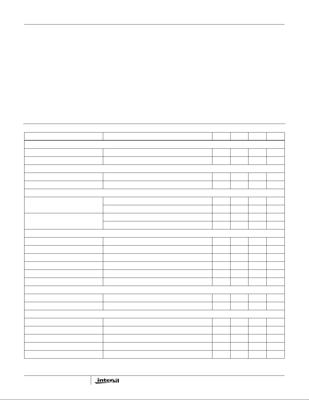
Electrical Specifications Operating Conditions: VCC = 5V, T
= 0°C to 70°C. Unless Otherwise Specified.
A
PARAMETER TEST CONDITIONS MIN TYP MAX UNITS
VCC SUPPLY CURRENT
Nominal Supply VCC = 5VDC; EN = 5VDC; R
Shutdown Supply VCC = 5VDC; EN = 0VDC; R
= 100 kΩ ±1% 8.0 10.8 14.0 mA
T
= 100 kΩ ±1% 8.0 10.3 13.0 mA
T
SHUNT REGULATOR
VCC Voltage VCC tied to 12VDC thru 300Ω resistor, R
VCC Sink Current VCC tied to 12VDC thru 300Ω resistor, R
= 100kΩ 5.63 5.8 5.97 V
T
= 100kΩ 15 20 25 mA
T
POWER-ON RESET AND ENABLE
POR Threshold VCC Rising 4.25 4.35 4.50 V
VCC Falling 3.75 3.85 4.00 V
ENABLE Threshold EN Rising 1.205 1.23 1.255 V
Hysteresis 86 92 98 mV
REFERENCE VOLTAGE AND DAC
Reference Voltage 0.792 0.8 0.808 V
System Accuracy (Note 3) -1 - 1 %VID
VID on Fly Step Size R
= 100kΩ -25-mV
T
VID Pull Up --20-µA
VID Input Low Level --1V
VID Input High Level - 1.36 1.60 V
PIN-ADJUSTABLE OFFSET
OFS Current -100- µA
Offset Accuracy ROFS = 5.00kΩ ±1% 47.0 50.0 53.0 mV
OSCILLATOR
Accuracy -10 - 10 %
Adjustment Range 0.08 - 1.0 MHz
Disable Voltage I
= 1mA 0.8 1.0 1.2 V
FS/DIS
Sawtooth Amplitude -1.37- V
Max Duty Cycle -75-%
4
FN9084.8
December 29, 2004
ISL6559
Electrical Specifications Operating Conditions: VCC = 5V, T
= 0°C to 70°C. Unless Otherwise Specified. (Continued)
A
PARAMETER TEST CONDITIONS MIN TYP MAX UNITS
ERROR AMPLIFIER
Open-Loop Gain R
Open-Loop Bandwidth C
Slew Rate C
Maximum Output Voltage R
= 10kΩ to ground - 72 - dB
L
= 100pF, RL = 10kΩ to ground - 18 - MHz
L
= 100pF, Load = ±400mA - 7.1 11 V/µs
L
= 10kΩ to ground 3.6 4.5 - V
L
Source Current 3.0 7.0 9.5 mA
Sink Current 1.6 3.0 5.4 mA
REMOTE-SENSE AMPLIFIER
Input Impedance -80-kΩ
Bandwidth -20-MHz
Slew Rate -6-V/µs
SENSE CURRENT
IOUT Accuracy ISEN1 = ISEN2 = ISEN3 = ISEN4 = 50µA -5 - 5 %
ISEN Offset Voltage -6-mV
Over-Current Trip Level 72 90 108 µA
POWER GOOD AND PROTECTION MONITORS
PGOOD Low Voltage I
= 4mA - - 0.4 V
PGOOD
Under-Voltage Offset From VID VSEN Falling 320 350 420 mV
Over-Voltage Threshold VSEN Rising 2.08 2.13 2.20 V
OVP Voltage I
= 100mA, VCC = 5V 2.2 3.28 4.0 V
OVP
NOTE:
3. These parts are designed and adjusted for accuracy within the system tolerance
Functional Pin Description
VID2
VID1
VID0
NC
OFS
COMP
FB
NC
ISL6559CR (32 LEAD QFN)ISL6559CB (28 LEAD SOIC)
TOP VIEW
VID3NCVID4
32 31 30 29 28 27 26 25
1
2
3
4
5
6
7
8
9 10111213141516
IOUT
NC = NO CONNECT
OVP
GNDENFS/DIS
GND
VSEN
VDIFF
RGND
GND
VCC
TOP VIEW
28
27
26
25
24
23
22
21
20
19
18
17
16
15
EN
FS/DIS
PGOOD
PWM4
ISEN4
ISEN1
PWM1
PWM2
GND
ISEN2
ISEN3
PWM3
VCC
GND
GND
OVP
VID4
VID3
VID2
VID1
VID0
OFS
COMP
FB
IOUT
VDIFF
VSEN
RGND
1
2
3
4
5
6
7
8
9
10
11
12
13
14
GND
Bias and reference ground for the IC.
OVP
Over-voltage protection pin. This pin pulls to VCC and is
latched when an over-voltage condition is detected. Connect
PGOOD
PWM4
24
ISEN4
23
ISEN1
22
PWM1
21
PWM2
20
GND
19
ISEN2
18
ISEN3
17
PWM3
this pin to the gate of an SCR or MOSFET tied across V
IN
and ground to prevent damage to a load device.
VID4, VID3, VID2, VID1, VID0
The state of these five inputs program the internal DAC,
which provides the reference voltage for output regulation.
Connect these pins to either open-drain or active pull-up
type outputs. Pulling these pins above 2.9V can cause a
reference offset inaccuracy.
OFS
Connecting a resistor between this pin and ground creates a
positive offset voltage which is added to the DAC voltage,
allowing easy implementation of load-line regulation. For no
offset, simply tie this pin to ground.
FB and COMP
The internal error amplifier inverting input and output
respectively. Connect the external R-C feedback
compensation network of the regulator to these pins.
IOUT
The current carried out of this pin is proportional to output
current and can be used to incorporate output voltage droop
5
FN9084.8
December 29, 2004
ISL6559
and/or load sharing. The scale f actor is set b y the r atio of th e
ISEN resistors and the lower MOSFET r
DS(ON)
. If droop is
desired, connect this pin to FB. When not used for droop or
load sharing, simply leave this pin open.
VSEN, RGND, VDIFF
VSEN and RGND are the inputs to the differential remotesense amplifier. Connect these pins to the sense points of
the remote load. Connect an appropriately sized feedback
resistor, R
, between VDIFF and FB.
FB
VCC
Supplies all the power necessary to operate the chip. The IC
starts to operate when the voltage on this pin exceeds the
rising POR threshold and shuts down when the voltage on
this pin drops below the falling POR threshold. Connect this
pin directly to a +5V supply or through a series 300Ω resistor
to a +12V supply.
ISEN1, ISEN2, ISEN3, ISEN4
Current sense inputs. A resistor connected between these
pins and their respective phase node sets a current
proportional to the current in the lower MOSFET during it’s
conduction interval. This current is used as a reference for
channel balancing, load sharing, protection, and load-line
regulation. Inactive channels should have their respective
sense inputs left open.
PWM1, PWM2, PWM3, PWM4
Pulse-width modulating outputs. Connect these pins to the
individual HIP660x driver PWM input pins. These logic
outputs command the driver IC(s) in switching the halfbridge configuration of MOSFETs.The number of active
channels is determined by the state of PWM3 and PWM4. If
PWM3 is tied to VCC, this indicates to the controller that two
channel operation is desired. In this case, PWM 4 should be
left open or tied to VCC. Shorting PWM4 to VCC indicates
that three channel operation is desired.
PGOOD
Power good is an open-drain logic output that changes to a
logic low when the voltage at VDIFF is 350mV below the VID
setting or above 2.2V.
FS/DIS
A dual function pin for setting the switching frequency and
disabling the controller. Place a resistor from this pin to
ground to set the switching frequency between 80kHz and
1MHz. Pulling this pin below 0.8V disables the controller.
EN
Threshold sensitive enable input of the controller. Transition
this pin above 1.23V (typical enable threshold) to initiate a
soft-start cycle. Pull this pin below 1.14V , taking into account
the enable hysteresis, to disable the controller once in
operation. Connect a resistor divider to this pin to set the
power-on voltage level for proper coordination with Intersil
MOSFET drivers. If this function is not required, simply tie
this pin to VCC.
Multi-Phase Power Conversi on
Microprocessor load current profiles have changed to the
point where the multi-phase power conversion advantage is
pronounced. The technical challenges associated with
producing a single-phase converter which is both costeffective and thermally viable have forced a change to the
cost-saving approach of multi-phase. The ISL6559 controller
helps reduce the complexity of implementation by integrating
vital functions and requiring minimal output components.
The block diagram in Figure 1 provides a top level view of
multi-phase power conversion using the ISL6559 controller.
Interleaving
The switching of each channel in a multi-phase converter is
timed to be symmetrically out of phase with each of the other
channels. In a 3-phase converter, each channel switches 1/3
cycle after the previous channel and 1/3 cycle before the
following channel. As a result, the three-phase converter has
a combined ripple frequency three times greater than the
ripple frequency of any one phase. In addition, the peak-topeak amplitude of the combined inductor currents is reduced
in proportion to the number of phases (Equations 1 and 2).
Increased ripple frequency and lower ripple amplitude mean
that the designer can use less per-channel inductance and
lower total output capacitance for any performance
specification.
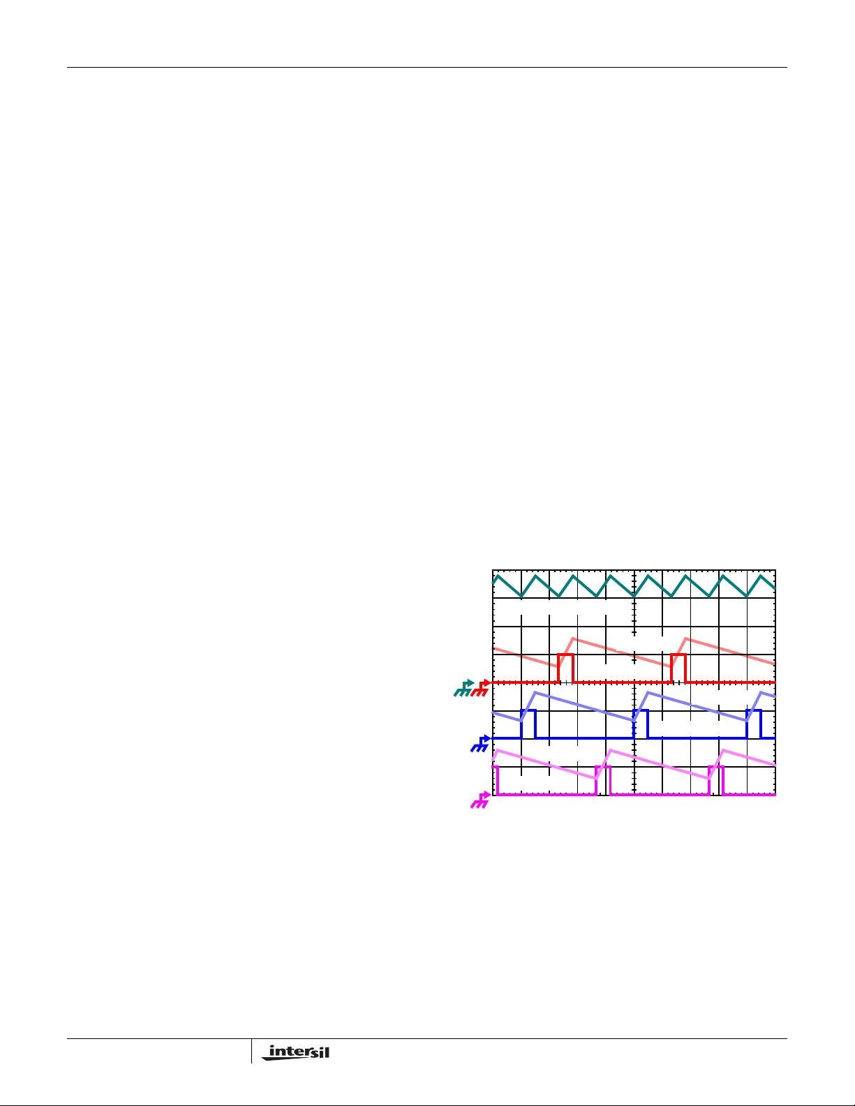
IL1 + IL2 + IL3, 7A/DIV
IL3, 7A/DIV
PWM3, 5V/DIV
IL2, 7A/DIV
PWM2, 5V/DIV
IL1, 7A/DIV
PWM1, 5V/DIV
1µs/DIV
FIGURE 1. PWM AND INDUCTOR-CURRENT WA VEFORMS
FOR 3-PHASE CONVERTER
Figure 1 illustrates the multiplicative effect on output ripple
frequency. The three channel currents (IL1, IL2, and IL3),
combine to form the AC ripple current and the DC load
current. The ripple component has three times the ripple
frequency of each individual channel current. Each PWM
pulse is terminated 1/3 of a cycle, or 1.33µs, after the PWM
pulse of the previous phase. The peak-to-peak current
waveforms for each phase is about 7A, and the dc
components of the inductor currents combine to feed the load.
6
FN9084.8
December 29, 2004
ISL6559
To understand the reduction of ripple current amplitude in
the multi-phase circuit, examine the equation representing
an individual channel’s peak-to-peak inductor current.
VINV
–()V
OUT
I
------------------------------------------------------=
PP
LfSV
In Equation 1, V
IN
and V
IN
OUT
are the input and output
OUT
(EQ. 1)
voltages respectively, L is the single-channel inductor value,
and f
is the switching frequency.
S
The output capacitors conduct the ripple component of the
inductor current. In the case of multi-phase converters, the
capacitor current is the sum of the ripple currents from each
of the individual channels. Compare Equation 1 to the
expression for the peak-to-peak current after the summation
of N symmetrically phase-shifted inductor currents in
Equation 2. Peak-to-peak ripple current decreases by an
amount proportional to the number of channels. Outputvoltage ripple is a function of capacitance, capacitor
equivalent series resistance (ESR), and inductor ripple
current. Reducing the inductor ripple current allows the
designer to use fewer or less costly output capacitors.
VINNV
–()V
OUT
I
------------------------------------------------------------=
CPP,
LfSV
OUT
IN
(EQ. 2)
Another benefit of interleaving is to reduce input ripple
current. Input capacitance is determined in part by the
maximum input ripple current. Multi-phase topologies can
improve overall system cost and size b y lowe ring input ripple
current and allowing the designer to reduce the cost of input
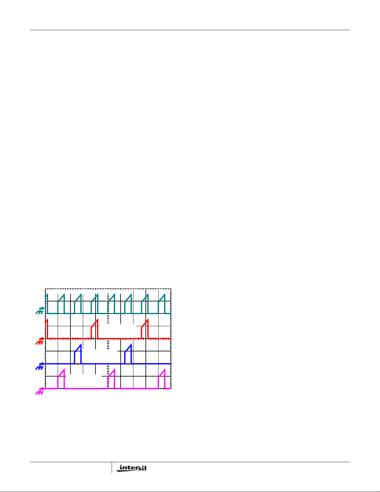
capacitance. The example in Figure 2 illustrates input
currents from a three-phase converter combining to reduce
the total input ripple current.
INPUT-CAPACITOR CURRENT, 10A/DIV
CHANNEL 3
INPUT CURRENT
10A/DIV
CHANNEL 2
INPUT CURRENT
10A/DIV
CHANNEL 1
INPUT CURRENT
10A/DIV
1µs/DIV
FIGURE 2. CHANNEL INPUT CURRENTS AND INPUT-
CAPACITOR RMS CURRENT FOR 3-PHASE
CONVERTER
The converter depicted in Figure 2 delivers 36A to a 1.5V
load from a 12V input. The RMS input capacitor current is
5.9A. Compare this to a single-phase converter also
stepping down 12V to 1.5V at 36A. The single-phase
converter has 11.9A RMS input capacitor current. The
single-phase converter must use an input capacitor bank
with twice the RMS current capacity as the equivalent threephase converter.
Figures 15, 16 and 17 in the section entitled Input Capacitor
Selection can be used to determine the input-capacitor RMS
current based on load current, duty cycle, and the number of
channels. They are provided as aids in determining the
optimal input capacitor solution. Figure 18 shows the single
phase input-capacitor RMS current for comparison.
PWM Operation
The timing of each converter leg is set by the number of
active channels. The default channel setting for the ISL6559
is four. One switching cycle is defined as the time between
PWM1 pulse termination signals. The pulse termination
signal is an internally generated clock signal which triggers
the falling edge of PWM1. The cycle time of the pulse
termination signal is the inverse of the switching frequency
set by the resistor between the FS/DIS pin and ground. Each
cycle begins when the clock signal commands the channel-1
PWM output to go low. The PWM1 transition signals the
channel-1 MOSFET driver to turn off the channel-1 upper
MOSFET and turn on the channel-1 synchronous MOSFET.
In the default channel configuration, the PWM2 pulse
terminates 1/4 of a cycle after PWM1. The PWM 3 output
follows another 1/4 of a cycle after PWM2. PWM4 terminates
another 1/4 of a cycle after PWM3.
If PWM3 is connected to VCC, then two channel operation is
selected and the PWM2 pulse terminates 1/2 of a cycle later.
Connecting PWM4 to VCC selects three channel operation
and the pulse-termination times are spaced in 1/3 cycle
increments.
Once a PWM signal transitions low, it is held low for a
minimum of 1/4 cycle. This forced off time is required to
ensure an accurate current sample. Current sensing is
described in the next section. After the forced off time
expires, the PWM output is enabled. The PWM output state
is driven by the position of the error amplifier output signal,
V
, minus the current correction signal relative to the
COMP
sawtooth ramp as illustrated in Figure 1. When the modified
V
voltage crosses the sawtooth ramp, the PWM output
COMP
transitions high. The MOSFET driver detects the change in
state of the PWM signal and turns off the synchronous
MOSFET and turns on the upper MOSFET. The PWM signal
will remain high until the pulse termination signal marks the
beginning of the next cycle by triggering the PWM signal low.
Current Sensing
During the forced off time following a PWM transition low , the
controller senses channel load current by sampling the
voltage across the lower MOSFET r
ground-referenced amplifier, internal to the ISL6559,
connects to the PHASE node through a resistor, R
voltage across R
is equivalent to the voltage drop
ISEN
, see Figure 3. A
DS(ON)
ISEN
. The
7
FN9084.8
December 29, 2004
 Loading...