

Page 1
®
ISL6557A
Data Sheet July 2004
Multi-Phase PWM Controller for
Core-Voltage Regulation
The ISL6557A provides core-voltage regulation by driving up
to four interleaved synchronous-rectified buck-converter
channels in parallel. Intersil multi-phase controllers together
with Intersil MOSFET drivers form the basis for the most
reliable power-suppply solutions available to pow er the latest
industry-leading microprocessors. Multi-phase buck
converter architecture uses interleaved timing to multiply
ripple frequency and reduce input and output ripple currents.
Lower ripple results in lower total component cost, reduced
dissipation, and smaller implementation area. Preconfigured for 4-phase operation, the ISL6557A offers the
flexibility of selectable 2- or 3-phase operation. Simply
connect the unused PWM pins to VCC. The channel
switching frequency is adjustable in the range of 50kHz to
igMHz giving the designer the ultimate flexibility in managing
the balance between high-speed response and good
thermal management.
New features on the ISL6557A include Dynamic-VID™
technology allowing seamless on-the-fly VID changes with
no need for any additional external components. When the
ISL6557A receives a new VID code, it incrementally steps
the output voltage to the new level. Dynamic VID changes
are fast and reliable with no output voltage overshoot or
undershoot. The RGND and VSEN pins provide inputs for
differential remote voltage sensing to improve regulation and
protection accuracy. A threshold-sensitive enable pin (EN)
can be used with an external resistor divider to optionally set
the power-on voltage level. This allows optional star t-up
coordination with Intersil MOSFET drivers or any other
devices powered from a separate supply.
Like other Intersil multiphase controllers, the ISL6557A uses
cost and space-saving r
balance, dynamic voltage positioning, and overcurrent
protection. Channel current balancing is automatic and
accurate with the integrated current-balance control system.
Overcurrent protection can be tailored to any application with
no need for additional parts. The IOUT pin carries a signal
proportional to load current and can be optionally connected
to FB for accurate load-line regulation.
An integrated DAC decodes the 5-bit logic signal present at
VID4-VID0 and provides an accurate reference for precision
voltage regulation. The high-bandwidth error amplifier,
differential remote-sensing amplifier, and accurate voltage
reference all work together to provide better than 0.8% total
system accuracy, and to enable the fastest transient
response available.
sensing for channel current
DS(ON)
FN9068.3
Features
• Multi-Phase Power Conversion
• Active Channel Current Balancing
• Precision r
DS(ON)
Current Sensing
-Low Cost
- Lossless
• Precision CORE Voltage Regulation
- Differential Remote Voltage Sensing
- ±0.8% System Accuracy
• Microprocessor Voltage Identification Input
- Dynamic VID technology
- 5-Bit VID Input
- 0.800V to 1.550V in 25mV Steps
• Programmable Power-On Bias Level
• Programmable Droop Voltage
• Fast Transient Recovery Time
• Precision Enable Threshold
• Overcurrent Protection
• 2-, 3-, or 4-Phase Operation
• High Ripple Frequency. Channel Frequency Times
Number Channels (100kHz to 6MHz)
• Pb-free available
Ordering Information
PART NUMBER TEMP. (oC) PACKAGE PKG. DWG. #
ISL6557ACB 0 to 70 24-Ld SOIC M24.3
ISL6557ACBZ
(See Note)
*Add “-T” suffix to part number for tape and reel packaging.
NOTE: Intersil Pb-free products employ special Pb-free material sets; molding
compounds/die attach materials and 100% matte tin plate termination finish, which
is compatible with both SnPb and Pb-free soldering operations. Intersil Pb-free
products are MSL classified at Pb-free peak reflow temperatures that meet or exceed
the Pb-free requirements of IPC/JEDEC J Std-020B.
0 to 70 24-Ld SOIC
(Pb-free)
M24.3
Pinout
ISL6557A 24 PIN (SOIC)
TOP VIEW
VID4
VID3
VID2
VID1
VID0
COMP
FB
IOUT
VDIFF
VSEN
RGND
GND
1
2
3
4
5
6
7
8
9
10
11
12
24
23
22
21
20
19
18
17
16
15
14
13
VCC
EN
FS
PGOOD
PWM4
ISEN4
ISEN1
PWM1
PWM2
ISEN2
ISEN3
PWM3
1
All other trademarks mentioned are the property of their respective owners. Dynamic VID™ is a trademark of Intersil Americas Inc.
CAUTION: These devices are sensitive to electrostatic discharge; follow proper IC Handling Procedures.
1-888-INTERSIL or 321-724-7143
| Intersil (and design) is a trademark of Intersil Americas Inc.
Copyright © Intersil Americas Inc. 2003, 2004. All Rights Reserved.
Page 2
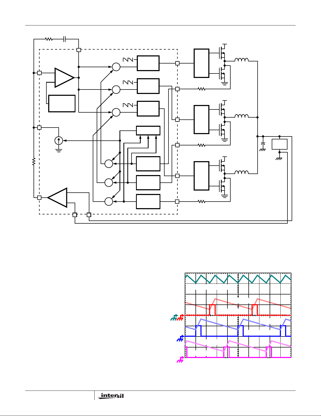
Block Diagram
ISL6557A
RGND
VSEN
COMP
VID0
VID1
VID2
VID3
VID4
-
+
x 0.9
2.5V
DYNAMIC
VID
D/A
VDIFF
x1
-
UV
+
+
OVP
-
PGOOD
S
OV
LATCH
+
∑
-
2.1V
SOFT-
START
AND FAULT
LOGIC
+
-
E/A
+
POWER-ON
RESET (POR)
∑
-
+
∑
VCC
CLOCK AND
SAWTOOTH
GENERATOR
-
+
∑
-
+
-
+
-
+
-
+
-
PWM
PWM
PWM
PWM
1.23V
-
+
EN
FS
PWM1
PWM2
PWM3
PWM4
FB
IOUT
I_TOT
OC
CURRENT
CORRECTION
I
OC
∑
+
+
+
+
GND
-
+
PHASE
NUMBER
CHANNEL
DETECTOR
ISEN1
ISEN2
ISEN3
ISEN4
2
Page 3
ISL6557A
Typical Application - 4-Phase Buck Converter
+12V
VIN
PGOOD
VID4
VID3
VID2
VID1
VID0
RT
IOUT
FB COMP
VDIFF
VSEN
RGND
ISL6557A
FS
VCC
ISEN1
PWM1
PWM2
ISEN2
PWM3
ISEN3
PWM4
ISEN4
GND
EN
+5V
PVCC
PWM
+12V
PVCC
PWM
+12V
PVCC
PWM
VCC BOOT
HIP6601A
DRIVER
VCC BOOT
HIP6601A
DRIVER
VCC BOOT
HIP6601A
DRIVER
UGATE
PHASE
LGATE
GND
VIN
UGATE
PHASE
LGATE
GND
VIN
µP
LOAD
UGATE
PHASE
LGATE
GND
+12V
VIN
VCC BOOT
PVCC
PWM
HIP6601A
DRIVER
UGATE
PHASE
LGATE
GND
3
Page 4

ISL6557A
Absolute Maximum Ratings
Supply Voltage, VCC . . . . . . . . . . . . . . . . . . . . . . . . . . . . . . . . . . .7V
Input, Output, or I/O Voltage . . . . . . . . . . GND -0.3V to V
ESD Classification . . . . . . . . . . . . . . . . . . . . . . . . . . . . . . . . . . 1.5kV
CC
+ 0.3V
Recommended Operating Conditions
Supply Voltage. . . . . . . . . . . . . . . . . . . . . . . . . . . . . . . . . . +5V ±5%
Ambient Temperature. . . . . . . . . . . . . . . . . . . . . . . . . . . 0
CAUTION: Stress above those listed in “Absolute Maximum Ratings” may cause permanent damage to the device. This is a stress only rating and operation of the
device at these or any other conditions above those indicated in the operational section of this specification is not implied.
NOTE:
is measured with the component mounted on a high effective thermal conductivity test board in free air. (See Tech Brief TB379 for details.)
1. θ
JA
Electrical Specifications Operating Conditions: V
PARAMETER TEST CONDITIONS MIN TYP MAX UNITS
INPUT SUPPLY POWER
Input Supply Current RT = 100kΩ, EN = 5V 10.5 15 mA
RT = 100kΩ, EN = 0V 5 9.2 mA
Power-On Reset Threshold VCC Rising 4.25 4.38 4.5 V
VCC Falling 3.75 3.86 4.0 V
Enable Threshold EN Rising 1.206 1.230 1.254 V
EN Falling 1.106 1.15 1.194 V
Enable Hysteresis 60 100 mV
Enable Current EN = 3V 50 nA
SYSTEM ACCURACY
System Accuracy (Note 2) -0.8 0.8 %VID
VID Pull Up -40 -20 -10 µA
VID Input Low Level 0.8 V
VID Input High Level (Note 3) 2.0 V
OSCILLATOR
Accuracy -20 20 %
Frequency RT = 110kΩ (±1%) 250 kHz
Adjustment Range 80 1500 kHz
Sawtooth Amplitude 1.33 V
Duty-Cycle Range 075%
ERROR AMPLIFIER
Open-Loop Gain RL = 10kΩ to ground 72 dB
Open-Loop Bandwidth CL = 100pF, RL = 10kΩ to ground 18 MHz
Slew Rate CL = 100pF, RL = 10kΩ to ground 5 V/µs
Maximum Output Voltage RL = 10kΩ to ground 3.6 4.1 V
REMOTE-SENSE AMPLIFIER
Input Impedance 80 kΩ
Slew Rate 6V/µs
Bandwidth 10 MHz
o
C to 70oC
= 5V, TA = 0oC to 70oC, Unless Otherwise Specified.
CC
Thermal Information
Thermal Resistance (Typical, Note 1) θJA (oC/W)
SOIC Package . . . . . . . . . . . . . . . . . . . . . . . . . . . . . 65
Maximum Junction Temperature . . . . . . . . . . . . . . . . . . . . . . .150
Maximum Storage Temperature Range. . . . . . . . . . -65
Maximum Lead Temperature (Soldering 10s) . . . . . . . . . . . . .300
(SOIC - Lead Tips Only)
o
C to 150oC
o
o
C
C
4
Page 5
ISL6557A
Electrical Specifications Operating Conditions: V
PARAMETER TEST CONDITIONS MIN TYP MA X UNITS
ISEN
Overcurrent Trip Level -90 -75 -60 µA
PROTECTION and MONITOR
Overvoltage Threshold VSEN Rising 2.04 2.09 2.13 V
VSEN Falling VID V
Undervoltage Threshold VSEN Rising 92 %VID
VSEN Falling 90 %VID
PGOOD Low Voltage IPGOOD = 4mA 0.18 0.4 mV
NOTES:
2. These parts are designed and adjusted for accuracy within the system tolerance given in the Electrical Specifications. The system tolerance
accounts for offsets in the differential and error amplifiers; reference-voltage inaccuracies; temperature drift; and the full DAC adjustment range.
3. VID input levels above 2.9V may produce an reference-voltage offset inaccuracy.
= 5V, TA = 0oC to 70oC, Unless Otherwise Specified. (Continued)
CC
Functional Pin Descriptions
1
VID4
2
VID3
3
VID2
4
VID1
5
VID0
6
COMP
7
FB
8
IOUT
9
VDIFF
10
VSEN
11
RGND
12 13
GND
24
23
22
21
20
19
18
17
16
15
14
VCC
EN
FS
PGOOD
PWM4
ISEN4
ISEN1
PWM1
PWM2
ISEN2
ISEN3
PWM3
VID4, VID3, VID2, VID1, VID0 (Pins 1, 2, 3, 4, 5)
These are the inputs to the internal DAC that provides the
reference voltage for output regulation. Connect these pi ns
to either open-drain or active-pull-up type outputs. Pulling
these pins above 2.9V can cause a reference offset
inaccuracy.
FB (Pin 7) and COMP (Pin 6)
The internal error amplifier’s inverting input and output
respectively. These pins are connected to an external R-C
network to compensate the regulator.
IOUT (Pin 8)
The current out of this pin is proportional to output current
and is used for load-line regulation and load sharing. The
scale factor is set by the ratio of the ISEN resistors
(connected to pins 14, 15, 18, and 19) to the lower MOSFET
r
DS(ON)
.
VDIFF (Pin 9), VSEN (Pin 10), RGND (Pin 11)
VSEN and RGND are the inputs to the differential remotesense amplifier. VDIFF is the output and it serves as the
input to the external regulation circuitry and the intern al
protection circuitry. Connect VSEN and RGND to the sense
pins of the remote load.
GND (Pin 12)
Return for VCC and signal ground for the IC.
PWM3, PWM2, PWM1, PWM4 (Pins 13, 16, 17, 20)
Pulse-width modulation outputs. These logic outputs tell the
driver IC(s) when to turn the MOSFETs on and off.
ISEN3, ISEN2, ISEN1, ISEN4 (PINS 14, 15, 18, 19)
Current sense inputs. A resistor connected between these
pins and the respective phase nodes has a current
proportional to the current in the lower MOSFET during its
conduction interval. The current is used as a reference for
channel balancing, load sharing, protection, and load-line
regulation.
PGOOD (Pin 21)
PGOOD is an open-drain logic output that changes to a logic
low when the differential output voltage at VDIFF swings
below 90% of the DAC setting or above 2.1V.
FS (Pin 22)
This pin has two functions. A resistor placed from FS to
ground sets the switching frequency. There is an inverse
relationship between the value of the resistor and the
switching frequency . This pin can also be used to disable the
controller. To disable the controller, pull this pin below 1V.
EN (Pin 23)
This is the threshold-sensitive enable input for the controller .
To enable the controller, pull this pin above 1.23V.
VCC (Pin 24)
Bias supply voltage for the controller. Connect this pin to a
5V power supply.
5
Page 6
ISL6557A
FB
VDIFF
AMPLIFIER
REFERENCE
I
OUT
ERROR
-
+
DAC
&
+
x 1
-
COMP
VIN
L
1
+
PWM
CIRCUIT
-
+
PWM
CIRCUIT
-
+
PWM
CIRCUIT
-
AVERAGE
+
-
+
-
+
-
CURRENT
SENSE
CURRENT
SENSE
CURRENT
SENSE
PWM1
ISEN1
PWM2
ISEN2
PWM3
ISEN3
R
R
R
HIP6601A
ISEN1
HIP6601A
ISEN2
HIP6601A
ISEN3
VIN
VIN
L
2
V
OUT
µP
C
O
LOAD
L
3
VSENRGND
FIGURE 1. SIMPLIFIED BLOCK DIAGRAM OF THE ISL6557A IN A 3-PHASE CONVERTER
Operation
Multi-Phase Power Conversion
Multi-phase power conversion provides the most costeffective power solution when load currents are no longer
easily supported by single-phase converters. Although its
greater complexity presents additional technical challenges,
the multi-phase approach offers cost-saving advantages with
improved response time, superior ripple cancellation, and
excellent thermal distribution.
INTERLEAVING
The switching of each channel in a multi-phase converter is
timed to be symmetrically out of phase with each of the other
channels. In a 4-phase converter, each channel switches 1/4
cycle after the previous channel and 1/4 cycle before the
following channel. As a result, the four-phase converter has
a combined ripple frequency four times greater than the
ripple frequency of any one phase. In addition, the peak-topeak amplitude of the combined inductor currents is reduced
in proportion to the number of phases (Equations 1 and 2).
Increased ripple frequency and lower ripple amplitude mean
that the designer can use less per-channel inductance and
lower total output capacitance for any performance
specification.
IL1 + IL2 + IL3, 7A/DIV
IL3, 7A/DIV
PWM3, 5V/DIV
IL2, 7A/DIV
PWM2, 5V/DIV
IL1, 7A/DIV
PWM1, 5V/DIV
1µs/DIV
FIGURE 2. PWM AND INDUCTOR-CURRENT WA VEFORMS
FOR 3-PHASE CONVERTER
6
Page 7

1
ISL6557A
Figure 2 (previous page) illustrates the multiplicative effect
on output ripple frequency. The three channel currents (IL1,
IL2, and IL3), combine to form the AC ripple current and the
DC load current. The ripple component has three times the
ripple frequency of each individual channel current. Each
PWM pulse is terminated 1/3 of a cycle, or 1.33µs, after the
PWM pulse of the previous phase. The peak-to-peak current
waveforms for each phase is about 7A, and the DC
components of the inductor currents combine to feed the load.
To understand the reduction of ripple current amplitude in
the multi-phase circuit, examine the equation representing
an individual channel’s peak-to-peak inductor current.
VINV
–()V
OUT
------------------------------------------------------=
PP,
LfSV
In Equation 1, V
and V
IN
IN
OUT
are the input and output
OUT
(EQ.
voltages respectively, L is the single-channel inductor value,
and f
is the switching frequency.
S
VINNV
–()V
OUT
I
------------------------------------------------------------=
PP
LfSV
OUT
IN
(EQ. 2)
The output capacitors conduct the ripple component of the
inductor current. In the case of multi-phase converters, the
capacitor current is the sum of the ripple currents from each
of the individual channels. Compare Equation 1 to the
expression for the peak-to-peak current after the summation
of N symmetrically phase-shifted inductor currents in Equation 2. Peak-to-peak ripple current decreases by an amount
proportional to the number of channels. Output-voltage ripple
is a function of capacitance, capacitor equivalent series resistance (ESR), and inductor ripple current. Reducing the induc-
tor ripple current allows the designer to use fewer or less
costly output capacitors.
INPUT-CAPACITOR CURRENT, 10A/DIV
CHANNEL 3
INPUT CURRENT
10A/DIV
CHANNEL 2
INPUT CURRENT
10A/DIV
CHANNEL 1
INPUT CURRENT
10A/DIV
1µs/DIV
FIGURE 3. CHANNEL INPUT CURRENTS AND INPUT-
CAPACITOR RMS CURRENT FOR 3-PHASE
CONVERTER
Another benefit of interleaving is to reduce input ripple
current. Input capacitance is determined in part by the
maximum input ripple current. Multi-phase topologies can
improve overall system cost and size b y lowering input ripple
current and allowing the designer to reduce the cost of input
capacitance. The example in Figure 3 illustrates input
currents from a three-phase converter combining to reduce
the total input ripple current.
The converter depicted in Figure 3 delivers 36A to a 1.5V
load from a 12V input. The rms input capacitor current is
5.9A. Compare this to a single-phase converter also down
12V to 1.5V at 36A. The single-phase converter has 11.9A
rms input capacitor current. The single-phase converter
must use an input capacitor bank with twice the rms current
capacity as the equivalent three-phase converter.
Figures 15, 16 and 17 the section entitled Input Capacitor
Selection can be used to determine the input-capacitor rms
current based on load current, duty cycle, and the number of
channels. They are provided as aids in determining the
optimal input capacitor solution. Figure 18 shows the single
phase input-capacitor rms current for comparisson.
PWM OPERATION
The number of active channels selected determines the
timing for each channel. By default, the timing mode for the
ISL6557A is 4-phase. The designer can select 2-phase
timing by connecting PWM3 to VCC or 3-phase timing by
connecting PWM4 to VCC.
One switching cycle for the ISL6557A is defined as the time
between PWM1 pulse termination signals (the internal signal
that initiates a falling edge on PWM1). The cycle time is the
inverse of the switching frequency selected by the resistor
connected between the FS pin and ground (see Switching
Frequency). Each cycle begins when a clock signal
7
Page 8

ISL6557A
commands the channel-1 PWM output to go low. This
signals the channel-1 MOSFET driver to turn off the
channel-1 upper MOSFET and turn on the channel-1
synchronous MOSFET. If two-channel operation is selected,
the PWM2 pulse terminates 1/2 of a cycle later. If three
channels are selected the PWM2 pulse terminates 1/3 of a
cycle after PWM1, and the PWM3 output will follow after
another 1/3 of a cycle. When four channels are selected, the
pulse-termination times are spaced in 1/4 cycle increments.
Once a channel’s PWM pulse terminates, it remains low for a
minimum of 1/4 cycle. This forced off time is required to
assure an accurate current sample as described in Current
Sensing. Following the 1/4-cycle forced off time, the
controller enables the PWM output. Once enabled, the PWM
output transitions high when the sawtooth signal crosses the
adjusted error-amplifier output signal, V
COMP
as illustrated
in Figures 1 and 5. This is the signal for the MOSFET driver
to turn off the synchronous MOSFET and turn on the upper
MOSFET. The output will remain high until the clock signals
the beginning of the next cycle by commanding the PWM
pulse to terminate.
CURRENT SENSING
Intersil multi-phase controllers sense current by sampling the
voltage across the lower MOSFET during its conduction
interval. MOSFET r
sensing is a no-added-cost
DS(ON)
method to sense current for load-line regulation, channelcurrent balance, module current sharing, and overcurrent
protection. If desired, an independent current-sense resistor
in series with the lower-MOSFET source can serve as a
sense element in place of the MOSFET r
r
I
SEN
In
SAMPLE
&
HOLD
ISL6557A INTERNAL CIRCUIT EXTERNAL CIRCUIT
FIGURE 4. INTERNAL AND EXTERNAL CURRENT-SENSING
DS ON()
--------------------------
=
I
L
R
ISEN
-
+
CIRCUITRY
ISEN(n)
R
ISEN
CHANNEL N
LOWER MOSFET
DS(ON)
V
IN
CHANNEL N
UPPER MOSFET
ILr
+
.
I
L
DS ON()
The ISEN input for each channel uses a ground-referenced
amplifier to reproduce a signal proportional to the channel
current (Figure 4). After sufficient settling time, the sensed
current is sampled, and the sample is used for current
balance, load-line regulation and overcurrent protection. The
ISL6557A samples channel current once each cycle.
Figure 4 shows how the sampled current, I
the channel current I
. The circuitry in Figure 4 represents
L
, is created from
n
the current measurement and sampling circuitry for channel
n in an N-channel converter. This circuitry is repeated for
each channel in the converter but may not be active in
channels 3 and 4 depending on the particular
implementation (see PWM Operation).
CHANNEL-CURRENT BALANCE
Another benefit of multi-phase operation is the thermal
advantage gained by distributing the dissipated heat over
multiple devices and greater area. By doing this, the
designer avoids the complexity of driving multiple parallel
MOSFETs and the expense of using expensive heat sinks
and exotic magnetic materials.
In order to fully realize the thermal advantage, it is important
that each channel in a multi-phase converter be controlled to
deliver about the same current at any load level. Intersil
multi-phase controllers guarantee current balance by
comparing each channel’s current to the average current
delivered by all channels and making an appropriate
adjustment to each channel’s pulse width based on the error.
Intersil’s patented current-balance method is illustrated in
Figure 5 where the average of the 2, 3, or 4 sampled channel
currents combines with the channel 1 sample, I
an error signal I
pulse width commanded by V
unbalance and force I
. The filtered error signal modifies the
ER
toward zero.
ER
to correct any
COMP
, to create
1
In some circumstances, it may be necessary to deliberately
design some channel-current unbalance into the system. In
a highly compact design, one or two channels may be able to
cool more effectively than the other(s) due to nearby air flow
or heat sinking components. The other channel(s) may have
more difficulty cooling with comparatively less air flow and
heat sinking. The hotter channels may also be located close
to other heat-generating components tending to drive their
temperature even higher. In these cases, a proper selection
of the current sense resistors (R
in Figure 4) introduces
ISEN
channel current unbalance into the system. Increasing the
value of R
in the cooler channels and decreasing it in
ISEN
the hotter channels moves all channels into thermal balance
at the expense of current balance.
OVERCURRENT PROTECTION
The average current, I
in Figure 5, is continually
AVG
compared with a constant 75µA reference current. If the
average current at any time exceeds the reference current,
the comparator triggers the converter to shut down. All PWM
signals are placed in a high-impedance state which signals
the drivers to turn off both upper and lower MOSFETs. The
8
Page 9

ISL6557A
system remains in this state while the controller counts 2048
phase-clock cycles.
V
COMP
FIGURE 5. CHANNEL-1 PWM FUNCTION AND CURRENT-
NOTE: *Channels 3 and 4 are optional.
+
-
f(jω)
I
ER
+
SAWTOOTH SIGNAL
I
AVG
-
I
1
+
-
÷ N
BALANCE ADJUSTMENT
PWM1
I4 *
I
Σ
*
3
I
2
This is followed by a soft-start attempt (see Soft-Start). If the
soft-start attempt is successful, operation will continue as
normal. Should the soft-start attempt fail, the ISL6557A
repeats the 2048-cycle wait period and follows with another
soft-start attempt. This hiccup mode of operation continues
indefinitely as shown in Figure 6 as long as the controller is
enabled or until the overcurrent condition resolves.
OUTPUT CURRENT, 20A/DIV
amplifier eliminates voltage differences between local and
remote ground to provide a more accurate means of sensing
output voltage.
EXTERNAL CIRCUIT ISL6557A INTERNAL CIRCUIT
C
C
R
R
FB
+
V
DROOP
-
V
OUT
REMOTE
GROUND
C
COMP
FB
IOUT
VDIFF
VSEN
RGND
ERROR AMPLIFIER
I
AVG
+
-
DIFFERENTIAL
REMOTE-SENSE
AMPLIFIER
V
+
REFERENCE
VOLTAGE
COMP
FIGURE 7. OUTPUT -VOLT A GE AND LOAD-LINE
REGULATION
The integrating compensation network shown in Figure 7
assures that the steady-state error in the output voltage is
limited to the error in the reference voltage (output of the
DAC) plus offset errors in the remote-sense and error
amplifiers. Intersil specifies the guaranteed tolerance of the
ISL6557A and all Intersil controllers to include all variations
in the amplifiers and reference so that the output voltage
remains within the specified system tolerance.
0A
OUTPUT VOLTAGE,
500mV/DIV
0V
5ms/DIV
FIGURE 6. OVERCURRENT BEHAVIOR IN HICCUP MODE
VOLTAGE REGULATION
The ISL6557A uses a digital to analog converter (DAC) to
generate a reference voltage based on the logic signals at
pins VID4 to VID0. The DAC decodes the a 5-bit logic signal
(VID) into one of the discrete voltages shown in Table 1. Each
VID input offers a 20µA pull up to 2.5V for use with open-drain
outputs. External pull-up resistors or active-high output
stages can augment the pull-up current sources, but a slight
accuracy error can occur if they are pulled above 2.9V.
.
The DAC-selected reference voltage is connected to the noninverting input of the error amplifier, and the output of the differential remote-sense amplifier usually gets connected to
the error amplifier as shown in Figure 7. The remote-sense
TABLE 1. VOLTAGE IDENTIFICATION CODES
VID4 VID3 VID2 VID1 VID0 VDAC
11111Off
111100.800
111010.825
111000.850
110110.875
110100.900
110010.925
110000.950
101110.975
101101.000
101011.025
101001.050
100111.075
100101.100
100011.125
100001.150
9
Page 10

ISL6557A
TABLE 1. VOLTAGE IDENTIFICATION CODES (Continued)
VID4 VID3 VID2 VID1 VID0 VDAC
011111.175
011101.200
011011.225
011001.250
010111.275
010101.300
010011.325
010001.350
001111.375
001101.400
001011.425
001001.450
000111.475
000101.500
000011.525
000001.550
OVERVOLTAGE PROTECTION
The ISL6557A detects output voltages above 2.1V and
immediately commands all PWM outputs low. This directs
the Intersil drivers turn on th e lower MOSFETs and protect
the load by preventing any further increase in output voltage.
Once the output voltage falls to the level set b y the VID code,
the PWM outputs enter high-impedance mode. The Intersil
drivers respond by turning off both upper and lower
MOSFETs. If the overvoltage condition reoccurs, the
ISL6557A will again command the lower MOSFETs to turn
on. The ISL6557A will continue to protect the load in this
fashion as long as the overvoltage repeats.
After detecting an overvoltage condition, the ISL6557A
ceases normal PWM operation until it is reset by power cycle
in which VCC is removed below the POR falling threshold
and restored above the POR rising threshold as described in
Enable and Disable and Electrical Specifications.
LOAD-LINE REGULATION
In applications with high transient current slew rates, the
lowest-cost soluti on for maintaining regulation often re quire s
some kind of controlled output impedance. Pin 8 of the
ISL6557A carries a current proportional to the average
current of all active channels. The current is equivalent to
I
in Figures 5 and 7. Connecting FB and IOUT together
AVG
forces I
produces a voltage drop across the feedback resistor, R
into the summing node of the error amplifier and
AVG
FB
proportional to the output current. In Figure 7, the steadystate value of V
V
DROOPIAVGRFB
DROOP
=
is simply
(EQ. 3)
In the case that each channel uses the same value for RISEN to
sense channel current, and this is almost always true, a more
complete expression for VDROOP can be determined from the
expression for IAVG as it is derived from Figures 4 and 5.
r
I
OUT
DS ON()
----------------------
AVG
DROOP
-------------
=
N
R
ISEN
r
I
OUT
DS ON()
----------------------
-------------
=
N
R
ISEN
R
FB
(EQ. 4)
I
V
ENABLE AND DISABLE
The internal power-on reset circuit (POR) prevents the
ISL6557A from starting before the bias voltage at VCC
reaches the POR-rising threshold as defined in Electrical
Specifications.The POR level is high enough to guarantee
that all parts of the ISL6557A can perform their functions
properly. Built-in hysteresis assures that once enabled, the
ISL6557A will not turn off unless the bias voltage falls to
approximately 0.5V below the POR-rising level. When VCC
is below the POR-rising threshold, the PWM outputs are held
in a high-impedance state to assure the drivers remain off.
EXTERNAL CIRCUITISL6557A INTERNAL CIRCUIT
+5V
VCC
ENABLE
COMPARATOR
POR
CIRCUIT
OV LATCH
SIGNAL
FIGURE 8. START-UP CONDITION USING THRESHOLD-
SENSITIVE ENABLE (EN) FUNCTION
+
-
1.23V (± 2%)
EN
+12V
10.7kΩ
1.40kΩ
After power on, the ISL6557A remains in shut-down mode
until the voltage at the enable input (EN) rises above 1.23V
(±2%). This optional feature prevents the ISL6557A from
operating until the connected voltage rail is available and
above some selectable threshold. For e xample, the HIP660X
family of MOSFET driver ICs require 12V bias, and in certain
circumstances, it can be important to assure that the drivers
reach their POR level before the ISL6557A becomes
enabled. The schematic in Figure 8 demonstrates
coordination of the ISL6557A with HIP660X family of
MOSFET driver ICs. The enable comparator has about
70mV of hysteresis to prevent bounce. To defeat the
threshold-sensitive enable, connect EN to VCC.
,
The 11111 VID code is reserved as a signal to the controller
that no load is present. The controller will ente r shut-down
mode after receiving this code and will start up upon
receiving any other code.
10
Page 11

ISL6557A
To enable the controller, VCC must be greater than the POR
threshold; the voltage on EN must be greater than 1.23V and
VID cannot be equal to 11111. Once these conditions are
true, the controller immediately initiates a soft start
sequence.
SOFT-START
The soft-start t i me, t
that increments with every pulse of the phase clock. For
example, a converter switching at 250kHz has a soft-start
time of
2048
T
------------ - 8.2ms==
SS
f
SW
, is determined by an 11-bit counter
SS
(EQ. 5)
11
Page 12

t
ISL6557A
During the soft-start interval, the soft-start voltage, V
RAMP
,
increases linearly from zero to 140% of the programmed
DAC voltage. At the same time a current source, I
RAMP
, is
decreasing from 160µA down to zero. These signals are
connected as shown in Figure 9 (I
may or may not be
OUT
connected to FB depending on the par ticular application).
EXTERNAL CIRCUIT ISL6557A INTERNAL CIRCUIT
C
C
R
C
R
FB
FIGURE 9. RAMP CURRENT AND VOL TAGE FOR
COMP
FB
IOUT
VDIFF
REGULATING SOFT-START SLOPE
AND DURATION
ERROR AMPLIFIER
I
RAMP
I
AVG
-
+
V
RAMP
IDEAL DIODES
V
COMP
REFERENCE
VOLTAGE
The ideal diodes in Figure 9 assure that the controller tries
to regulate its output to the lower of either the reference
voltage or V
across R
FB
not be seen until V
RAMP
. Since I
creates an initial offset
RAMP
of RFB times 160µA, the first PWM pulses will
is greater than the R
RAMP
FB
I
RAMP
offset. This produces a delay after the ISL6557A enables
before the output voltage starts moving. For example, if
VID = 1.5V, R
=1kΩ and TSS= 8.3ms, the delay time
FB
can be expressed using Equation 6.
T
t
DELAY
--------------------------------------------------- 580µs==
1
1.4 VID
---------------------------------------- -+
R
FB
SS
()
160 10
×
(EQ. 6)
–
6
leading to T
and t
RAMP2
FIGURE 10. SOFT -START WAVEFORMS FOR ISL6557A
NOTE: Switching frequency 500kHz and RFB = 2.67kΩ
= 4.0ms, t
SS
DELAY
= 700ns, t
RAMP1
= 2.23ms,
= 1.17ms.
VOUT, 500mV/DIV
EN, 5V/DIV
t
DELAYtRAMP1tRAMP2
BASED MULTI-PHASE BUCK CONVERTER
1ms/DIV
DYNAMIC VID
The ISL6557A is capable of executing on-the-fly outputvoltage changes. At the beginning of the phase-1 switching
cycle (defined in the section entitled PWM Operation), the
ISL6557A checks for a change in the VID code. The VID
code is the bit pattern present at pins VID4-VID0 as outlined
in Voltage Regulation. If the new code remains stable for
another full cycle, the ISL6557A begins incrementing the
reference by making 25mV change every two switching
cycles until the it reaches the new VID code.
01110 00010
VID, 5V/DIV
VID CHANGE OCCURS
ANYWHERE HERE
From this point, the soft start ramps linearly until V
reaches VID. F or the system described above , this first linear
ramp will continue for approximately
T
SS
t
RAMP1
=
---------- -
1.4
5.27ms=
t
–
DELAY
RAMP
(EQ. 7)
V
, 100mV/DIV
REF
1.3V
V
, 100mV/DIV
1.3V
OUT
The final portion of the soft-start sequence is the time
remaining after V
zero. This is also char acterized by a slight linear ramp in the
output voltage which, f or th e cu rrent example, exists for a time
RAMP2TSStRAMP1
– t
2.34ms=
This behavior is seen in the example in Figure 10 of a converter
switching at 500kHz. For this converter , R
reaches VID and before I
RAMP
–=
DELAY
RAMP
is set to 2.67kΩ
FB
gets to
(EQ. 8)
5µs/DIV
FIGURE 11. DYNAMIC-VID W AVEFORMS FOR 500KHZ
ISL6557A BASED MULTI-PHASE BUCK
CONVERTER
Since the ISL6557A recognizes VID-code changes only at
the beginnings of switching cycles, up to one full cycle may
pass before a VID change registers. This is followed by a
one-cycle wait before the output voltage begins to change.
Thus, the total time required for a VID change, t
DV
, is
12
Page 13

ISL6557A
dependent on the switching frequency (fS), the size of the
change (∆V
), and the time before the next switching cycle
ID
begins. The one-cycle uncertainty in Equation 9 is due to the
possibility that the VID code change may occur up to one full
cycle before being recognized. The time required for a
converter running with f
= 500kHz to make a 1.3V to 1.5V
S
reference-voltage change is between 30µs and 32µs as
calculated using Equation 9. This example is also illustrated
in Figure 11.
2V∆
2V∆
1
ID
---- -
-----------------
f
S
0.025
1–
t
DV
1
---- -
≤<
-----------------
f
0.025
S
ID
(EQ. 9)
General Design Guide
This design guide is intended to provide a hig h-level
explanation of the steps necessary to create a multi-phase
power conv erter . It is assumed that the rea der is familiar with
many of the basic skills and techniques ref eren ced below. In
addition to this guide, Intersil provides complete ref erence
designs that include schematics, bills of materials, and
example board la youts for all common microprocessor
applications.
Power Stages
The first step in designing a multi-phase converter is to
determine the number of phases. This determination
depends heavily on the cost analysis which in turn depends
on system constraints that differ from one design to the ne xt.
Principally, the designer will be concerned with whether
components can be mounted on both sides of the circuit
board; whether through-hole components are permitted on
either side; and the total board space available for powersupply circuitry. Generally speaking, the most economical
solutions will be for each phase to handle between 15 and
20A. All-surface-mount designs will tend toward the lower
end of this current range and, if through-hole MOSFETs can
be used, higher per-phase currents are possible. In cases
where board space is the limiting constraint, current can be
pushed as high as 30A per phase, but these designs require
heat sinks and forced air to cool the MOSFETs.
P
LOW 1,rDS ON()
I
M
----- -
N
2
1d–()
I
L
-------------------------------+=
2
1d–()
PP,
12
(EQ. 10)
An additional term can be added to the lower-MOSFET loss
equation to account for additional loss accrued during the
dead time when inductor current is flowing through the
lower-MOSFET body diode. This term is dependent on the
diode forward voltage at I
f
; and the length of dead times, td1 and td2, at the
S
, V
M
; the switching frequency ,
D(ON)
beginning and the end of the lower-MOSFET conduction
interval respectively.
P
LOW 2,
=
V
DON()fS
I
I
M
PP
----- -
-------- -+
N
2
I
M
t
+
----- -
d1
N
I
PP
-------- -–
2
(EQ. 11)
t
d2
Thus the total power dissipated in each lower MOSFET is
approximated by the summation of P
and PD.
L
UPPER MOSFET POWER CALCULATION
In addition to r
losses, a large portion of the upper-
DS(ON)
MOSFET losses are due to currents conducted across the
input voltage (V
) during switching. Since a substantially
IN
higher portion of the upper-MOSFET losses are dependant
on switching frequency, the power calculation is somewhat
more complex. Upper MOSFET losses can be divided into
separate components involving the upper-MOSFET
switching times; the lower-MOSFET body-diode reverserecovery charge, Q
; and the upper MOSFET r
rr
DS(ON)
conduction loss.
When the upper MOSFET turns off, the lower MOSFET does
not conduct any portion of the inductor current until the
voltage at the phase node falls below ground. Once the
lower MOSFET begins conducting, the current in the upper
MOSFET falls to zero as the current in the low er MOSFET
ramps up to assume the full inductor current. In Equation 12,
the required time for this commutation is t
associated power loss is P
≈
P
UP 1,VIN
I
M
----- -
N
I
L
PP,
-------------+
2
.
UP,1
t
1
f
----
S
2
and the
1
(EQ. 12)
MOSFETs
The choice of MOSFETs depends on the current each
MOSFET will be required to conduct; the switching frequency;
the capability of the MOSFETs to dissipate heat; and the
availability and nature of heat sinking and air flo w.
LOWER MOSFET POWER CALCULATION
The calculation for heat dissipated in the lower MOSFET is
simple, since virtually all of the heat loss in the lower
MOSFET is due to current conducted through the channel
resistance (r
continuous output current; I
current (see Equation 1); d is the duty cycle (V
L is the per-channel inductance.
). In Equation 10, IM is the maximum
DS(ON)
is the peak-to-peak inductor
L,PP
13
OUT/VIN
); and
Similarly, the upper MOSFET begins conducting as soon as
it begins turning on. In Equation 13, this transition occurs
over a time t
P
UP 2,VIN
, and the approximate the power loss is P
2
t
I
M
≈
----- -
N
I
2
L
PP,
-------------–
2
----
2
f
S
UP,2
(EQ. 13)
A third component involves the lower MOSFET’s reverserecovery charge, Q
. Since the inductor current has fully
rr
commutated to the upper MOSFET before the lowerMOSFET’s body diode can recover all of Q
, it is conducted
rr
through the upper MOSFET across VIN. The power
dissipated as a result is P
P
UP 3,
VINQrrf
=
S
and is simply
UP,3
(EQ. 14)
.
Page 14

ISL6557A
Finally, the resistive part of the upper MOSFET’s is given in
Equation 15 as P
P
UP 4,rDS ON()
In this case, of course, r
UP,4
I
M
----- -
N
.
2
d
+=
DS(ON)
2
I
PP
----------
12
is the on resistance of the
(EQ. 15)
upper MOSFET.
The total power dissipated by the upper MOSFET at full load
can now be approximated as the summation of the results
from Equations 12, 13, 14 and 15. Since the power
equations depend on MOSFET parameters, choosing the
correct MOSFETs can be an iterative process that involves
repetitively solving the loss equations for different MOSFETs
and different switching frequencies until conv erging upon the
best solution.
Current Sensing
Pins 18, 15, 14 and 19 are the ISEN pins denoted ISEN1,
ISEN2, ISEN3 and ISEN4 respectively. The resistors
connected between these pins and the phase nodes
determine the gains in the load-line regulation loop and the
channel-current balance loop. Select the values for these
resistors based on the room temperature r
lower MOSFETs; the full-load operating current, I
DS(ON)
of the
; and the
FL
number of phases, N according to Equation 16 (see also
Figure 4).
R
ISEN
r
DS ON()
-----------------------
=
50 10
I
FL
--------
–
6
N
×
(EQ. 16)
In certain circumstances, it may be necessary to adjust the
value of one or more of the ISEN resistors. This can arise
when the components of one or more channels are inhibited
from dissipating their heat so that the affected channel s run
hotter than desired (see the section entitled Channel-Current
Balance). In these cases, chose new , smaller v alues of R
for the aff ected phases. Choose R
in proportion to the
ISEN,2
ISEN
desired decrease in temperature rise in order to cause
proportionally less current to flow in the hotter phase.
∆T
ISEN 2,
=
ISEN
∆T
1
is the desired temperature
2
R
In Equation 17, make sure that ∆T
2
----------
R
rise above the ambient temperature , and ∆T
is the measured
1
(EQ. 17)
temperature rise above the ambient temperature. Whi le a
single adjustment according to Equation 17 is usually
sufficient, it may occasionally be necessary to adjust R
ISEN
two or more times to achiev e perfect thermal balance between
all channels.
Load-Line Regulation Resistor
The load-line regulation resistor is labeled RFB in Figure 7.
Its value depends on the desired full-load droop voltage
(V
in Figure 7). If Equation 16 is used to select each
DROOP
ISEN resistor, the load-line regulation resistor is as shown
in Equation 18.
V
FB
DROOP
------------------------ -=
50 106–×
(EQ. 18)
R
If one or more of the ISEN resistors was adjusted for thermal
balance as in Equation 17, the load-line regulation resistor
should be selected according to Equation19 where I
full-load operating current and R
connected to the n
V
DROOP
--------------------------------
R
=
FB
IFLr
th
DS ON()
ISEN pin.
R
∑
ISEN n()
n
is the ISEN resistor
ISEN(n)
is the
FL
(EQ. 19)
Compensation
The two opposing goals of compensating the voltage
regulator are stability and speed. Depending on whether the
regulator employs the optional load-line regulation as
described in Load-Line Regulation, there are two distinct
methods for achieving these goals.
COMPENSATING A LOAD-LINE REGULATED
CONVERTER
The load-line regulated converter behaves in a similar
manner to a peak-current mode controller because the two
poles at the output-filter L-C resonant frequency split with
the introduction of current information into the control loop.
The final location of these poles is determined by the system
function, the gain of the current signal, and the value of the
compensation components, R
Since the system poles and zero are effected by the values
of the components that are meant to compensate them, the
solution to the system equation becomes fairly complicated.
Fortunately there is a simple approximation that comes very
close to an optimal solution. Treating the system as though it
were a voltage-mode regulator by compensating the L-C
poles and the ESR zero of the voltage-mode approximation
yields a solution that is always stable with very close to ideal
transient performance.
C2 (OPTIONAL)
R
C
+
R
FB
V
DROOP
-
FIGURE 12. COMPENSATION CONFIGURATION FOR
LOAD-LINE REGULATED ISL6557A CIRCUIT
C
C
and CC.
C
COMP
IOUT
VDIFF
FB
ISL6557A
14
Page 15

C
ISL6557A
The feedback resistor, RFB, has already been chosen as outlined in Load-Line Regulation Resistor. Select a target band-
width for the compensated system, f0. The target bandwidth
must be large enough to assure adequate transient performance, but smaller than 1/3 of the per-channel switching frequency. The values of the compensation components
depend on the relationships of f
to the L-C pole frequency
0
and the ESR zero frequency. For each of the three cases
defined below, there is a separate set of equations for the
compensation components.
1
-------------------
>
Case 1:
Case 2:
Case 3:
2π LC
R
C
-------------------
2π LC
R
C
f
0
R
C
f
0
2π f0VppLC
----------------------------------- -
=
CRFB
0.75V
------------------------------------=
C
2π VPPRFBf
1
f
<≤
0
VPP2π()2f
--------------------------------------------
=
CRFB
-------------------------------------------------------------=
C
2π()2f
1
------------------------------
>
2π C ESR()
------------------------------------------
=
CRFB
C
0.75 V
0.75VINESR()C
-------------------------------------------------=
2π V
PPRFBf0
0.75V
IN
IN
0
1
------------------------------
2π CESR()
2
LC
0
0.75 V
IN
0.75V
IN
2
VPPRFBLC
0
2π f0VppL
ESR()
IN
L
(EQ. 20)
resonant frequency and a zero at the ESR frequency. A type
III controller, as shown in Figure 13, provides the necessary
compensation.
C
2
C
C
R
C
C
1
R
1
FIGURE 13. COMPENSATION CIRCUIT FOR ISL6557A B ASED
+
R
FB
V
DROOP
-
CONVERTER WITHOUT LOAD-LINE
REGULATION
COMP
FB
IOUT
ISL6557A
VDIFF
The first step is to choose the desired bandwidth, f0, of the
compensated system. Choose a frequency high enough to
assure adequate transient performance but not higher than
1/3 of the switching frequency. The type-III compensator has
an extra high-frequency pole, f
. This pole can be used for
HF
added noise rejection or to assure adequate attenuation at
the error-amplifier high-order pole and zero frequencies. A
good general rule is to chose f
if desired. Choosing f
to be lower than 10 f0 can cause
HF
=10f0, but it can be higher
HF
problems with too much phase shift below the system
bandwidth.
In Equations 20, L is the per-channel filter inductance
divided by the number of active channels; C is the sum total
of all output capacitors; ESR is the equivalent-series
resistance of the bulk output-filter capacitance; and V
PP
is
the peak-to-peak sawtooth signal amplitude as described in
Figure 5 and Electrical Specifications.
Once selected, the compensation values in Equations 20
assure a stable converter with reasonable transient performance. In most cases, transient performance can be
improved by making adjustments to R
value of R
while observing the transient performance on an
C
. Slowly increase the
C
oscilloscope until no further improvement is noted. Normally,
CC will not need adjustment. Keep the value of CC from
Equations 20 unless some performance issue is noted.
The optional capacitor C2, is sometimes needed to bypass
noise away from the PWM comparator (see Figure 5). Keep
a position available for C
, and be prepared to install a high-
2
frequency capacitor of between 22pF and 150pF in case any
jitter problem is noted.
COMPENSATION WITHOUT LOAD-LINE REGULATION
The non load-line regulated converter is accurately modeled
as a voltage-mode regulator with two poles at the L-C
In the solutions to the compensation equations, there is a
single degree of freedom. For the solutions presented in
Equations 21, R
is selected arbitrarily. The remaining
FB
compensation components are then selected according to
Equations 21.
CESR()
R1R
C
1
C
2
R
C
C
-----------------------------------------
=
FB
LC C ESR()–
LC C ESR()–
-----------------------------------------=
R
FB
0.75V
------------------------------------------------------------------ -=
2π()2f0fHFLCRFBV
RFBVPP2π
----------------------------------------------------------------=
0.75V
0.75VIN2π fHFLC 1–
-------------------------------------------------------------------=
2
2π
IN
2
2π fHFLC 1–
IN
VPPRFBf0fHFLC
(EQ. 21)
PP
f0fHFLC
15
Page 16

ISL6557A
In Equations 21, L is the per-channel filter inductance
divided by the number of active channels; C is the sum total
of all output capacitors; ESR is the equivalent-series
resistance of the bulk output-filter capacitance; and V
PP
is
the peak-to-peak sawtooth signal amplitude as described in
Figure 5 and “Electrical Specifications”.
Output Filter Design
The output inductors and the output capacitor bank together
form a low-pass filter responsible for smoothing the pulsating
voltage at the phase nodes. The output filter also must
provide the transient energy during the interval of time after
the beginning of the transient until the regulator can fully
respond. Because it has a low bandwidth compared to the
switching frequency, the output filter necessarily limits the
system transient response leaving the output capacitor bank
to supply or sink load current while the current in the output
inductors increases or decreases to meet the dema n d.
In high-speed converters, the output capacitor bank is
usually the most costly (and often the largest) part of the
circuit. Output filter design begins with minimizing the cost of
this part of the circuit. The critical load parameters in
choosing the output capacitors are the maximum size of the
load step, ∆I; the load-current slew rate, di/dt; and the
maximum allowable output-voltage de viation under transient
loading, ∆V
their capacitance, ESR, and ESL (equivalent series
inductance).
At the beginning of the load transient, the output capacitors
supply all of the transient current. The output voltage will
initially deviate by an amount approximated by the voltage
drop across the ESL. As the load current increases, the
voltage drop across the ESR increases linearly until the load
current reaches its final value. The capacitors selected must
have sufficiently low ESL and ESR so that the total outputvoltage deviation is less than the allowable maximum.
Neglecting the contribution of inductor current and regulator
response, the output voltage initially deviates by an amount
∆V ESL()
The filter capacitor must have sufficiently low ESL and ESR
so that ∆V < ∆V
Most capacitor solutions rely on a mixture of high-frequency
capacitors with relatively low capacitance in combination
with bulk capacitors having high capacitance but limited
high-frequency performance. Minimizing the ESL of the highfrequency capacitors allows them to support the output
voltage as the current increases. Minimizing the ESR of the
bulk capacitors allows them to supply the increased current
with less output voltage deviation.
. Capacitors are characterized according to
MAX
di
-----
ESR()∆I+≈
dt
.
MAX
(EQ. 22)
source the inductor ac ripple current (see Interleaving and
Equation 2), a voltage develops across the bulk-capacitor
ESR equal to I
(ESR). Thus, once the output capacitors
PP
are selected, the maximum allowable ripple voltage,
V
PP(MAX)
L ESR()
≥
, determines the a lower limit on the inductance.
V
–
INNVOUT
------------------------------------------------------------
fSVINV
V
OUT
PP MAX()
(EQ. 23)
Since the capacitors are supplying a decreasing portion of
the load current while the regulator recovers from the
transient, the capacitor voltage becomes slightly depleted.
The output inductors must be capable of assuming the entire
load current before the output voltage decreases more than
∆V
. This places an upper limits on inductance.
MAX
2NCV
---------------------
L
()
()
1.25
------------------------- -
L
≤
O
2
∆I
NC
2
()
∆I
∆V
∆V
MAX
MAX
∆I ESR()–≤
∆I ESR()– VINVO–
(EQ. 24)
(EQ. 25)
Equation 24 gives the upper limit on L for the cases when the
trailing edge of the current transient causes a greater outputvoltage deviation than the leading edge. Equation 25
addresses the leading edge. Normally, the trailing edge
dictates the selection of L because duty cycles are usually
less than 50%. Nevertheless, both inequalities should be
evaluated, and L should be selected based on the lower of
the two results. In each equation, L is the per-channel
inductance, C is the total output capacitance, and N is the
number of active channels.
Switching Frequency
There are a number of variables to consider when choosing
the switching frequency. There are considerable effects on
the upper-MOSFET loss calculation and, to a lesser extent,
the lower-MOSFET loss calculation. These effects are
outlined in MOSFETs, and they establish the upper limit for
the switching frequency. The lower limit is established by the
requirement for fast transient response and small outputvoltage ripple as outli ned in Output Filter Design. Choose the
lowest switching frequency that allows the regulator to meet
the transient-response requirements.
Switching frequency is determined by the selection of the
frequency-setting resistor,RT (see the figure Typical
The ESR of the bulk capacitors also creates the majority of
the output-voltage ripple. As the bulk capacitors sink and
16
Page 17

ISL6557A
Application on page 3). Figure 14 and Equation 26 are
provided to assist in the selecting the correct value for RT.
1000
100
RT (kΩ)
10
100 1000 1000010
SWITCHING FREQUENCY (KHZ)
FIGURE 14. RT VS SWITCHING FREQUENCY
[]
RT 10
=
11.09 1.13 fS()log–
(EQ. 26)
Input Capacitor Selection
The input capacitors are responsible for sourcing the ac
component of the input current flowing into the upper
MOSFETs. Their rms current capacity must be sufficient to
handle the ac component of the current drawn by the upper
MOSFETs which is related to duty cycle and the number of
active phases.
0.3
)
O
/ I
RMS
0.2
0.1
I
= 0
L,PP
= 0.5 I
I
L,PP
I
INPUT-CAPACITOR CURRENT ( I
L,PP
0
00.4 1.00.2 0.6 0.8
= 0.75 I
O
O
DUTY CYCLE ( V
IN
/ VO )
FIGURE 15. NORMALIZED INPUT -CAPA CITOR RMS CURRENT
VS DUTY CYCLE FOR 2-PHASE CONVERTER
0.3
I
= 0
L,PP
)
O
/ I
RMS
0.2
0.1
I
L,PP
= 0.25 I
O
I
L,PP
I
L,PP
= 0.5 I
= 0.75 I
O
O
Figures 15, 16 and 17 can be used to determine the inputcapacitor rms current as of duty cycle, maximum sustained
output current (I
peak inductor current (I
maximum sustained load current, I
), and the ratio of the combined peak-to-
O
as defined in Equation 1) to the
L,PP
. Figure 18 is provided
O
as a reference to demonstrate the dramatic reductions in
input-capacitor rms current upon the implementation of the
multiphase topology.
INPUT-CAPACITOR CURRENT ( I
0
00.4 1.00.2 0.6 0.8
DUTY CYCLE ( V
IN
/ VO )
FIGURE 16. NORMALIZED INPUT -CAPA CITOR RMS CURRENT
VS DUTY CYCLE FOR 3-PHASE CONVERTER
17
Page 18

ISL6557A
0.3
I
= 0
L,PP
)
O
/ I
RMS
0.2
0.1
INPUT-CAPACITOR CURRENT ( I
= 0.25 I
I
L,PP
0
00.4 1.00.2 0.6 0.8
O
I
L,PP
I
L,PP
DUTY CYCLE ( V
= 0.5 I
= 0.75 I
/ VO )
IN
O
O
FIGURE 17. NORMALIZED INPUT -CAPA CITOR RMS CURRENT
VS DUTY CYCLE FOR 4-PHASE CONVERTER
0.6
)
O
/ I
RMS
0.4
0.2
I
= 0
L,PP
= 0.5 I
I
L,PP
I
INPUT-CAPACITOR CURRENT ( I
0
00.4 1.00.2 0.6 0.8
L,PP
O
= 0.75 I
O
DUTY CYCLE ( V
IN
/ VO )
FIGURE 18. NORMALIZED INPUT -CAPA CITOR RMS CURRENT
VS DUTY CYCLE FOR SINGLE-PHASE
CONVERTER
18
Page 19

Small Outline Plastic Packages (SOIC)
ISL6557A
N
INDEX
AREA
123
SEA TING PLANE
-AD
e
B
0.25(0.010) C AM BS
M
E
-B-
A
-C-
0.25(0.010) BM M
H
α
µ
A1
0.10(0.004)
L
h x 45
o
C
NOTES:
1. Symbols are defined in the “MO Series Symbol List” in Section 2.2 of
Publication Number 95.
2. Dimensioning and tolerancing per ANSI Y14.5M-1982.
3. Dimension “D” does not include mold flash, protrusions or gate burrs.
Mold flash, protrusion and gate burrs shall not exceed 0.15mm
(0.006 inch) per side.
4. Dimension “E” does not include interlead flash or protrusions. Interlead flash and protrusions shall not exceed 0.25mm (0.010 inch) per
side.
5. The chamfer on the body is optional. If it is not present, a visual index
feature must be located within the crosshatched area.
6. “L” is the length of terminal for soldering to a substrate.
7. “N” is the number of terminal positions.
8. Terminal numbers are shown for reference only.
9. The lead width “B”, as measured 0.36mm (0.014 inch) or greater
above the seating plane, shall not exceed a maximum value of
0.61mm (0.024 inch)
10. Controlling dimension: MILLIMETER. Converted inch dimensions
are not necessarily exact.
M24.3 (JEDEC MS-013-AD ISSUE C)
24 LEAD WIDE BODY SMALL OUTLINE PLASTIC PACKAGE
INCHES MILLIMETERS
SYMBOL
A 0.0926 0.1043 2.35 2.65 -
A1 0.0040 0.0118 0.10 0.30 -
B 0.013 0.020 0.33 0.51 9
C 0.0091 0.0125 0.23 0.32 D 0.5985 0.6141 15.20 15.60 3
E 0.2914 0.2992 7.40 7.60 4
e 0.05 BSC 1.27 BSC H 0.394 0.419 10.00 10.65 h 0.010 0.029 0.25 0.75 5
L 0.016 0.050 0.40 1.27 6
N24 247
o
α
0
o
8
o
0
o
8
Rev. 0 12/93
NOTESMIN MAX MIN MAX
-
All Intersil U.S. products are manufactured, assembled and tested utilizing ISO9000 quality systems.
Intersil Corporation’s quality certifications can be viewed at www.intersil.com/design/quality
Intersil products are sold by description only. Intersil Corporation reserves the right to make changes in circuit design, software and/or specifications at any time without
notice. Accordingly, the reader is cautioned to verify that data sheets are current before placing orders. Information furnished by Intersil is believed to be accurate and
reliable. However, no responsibility is assumed by Intersil or its subsidiaries for its use; nor for any infringements of patents or other rights of third parties which may result
from its use. No license is granted by implication or otherwise under any patent or patent rights of Intersi l or its subs idiaries.
For information regarding Intersil Corporation and its products, see www.intersil.com
19
 Loading...