

Page 1

®
www.BDTIC.com/Intersil
ISL6551
Data Sheet January 3, 2006
ZVS Full Bridge PWM Controller
The ISL6551 is a zero voltage switching (ZVS) full-bridge
PWM controller designed for isolated power systems. This
part implements a unique control algorithm for fixedfrequency ZVS current mode control, yielding high efficiency
with low EMI. The two lower drivers are PWM-controlled on
the trailing edge and employ resonant delay while the two
upper drivers are driven at a fixed 50% duty cycle.
This IC integrates many features in both 6x6 mm
28-lead SOIC packages to yield a complete and
sophisticated power supply solution. Control features include
programmable soft-start for controlled start-up,
programmable resonant delay for zero voltage switching,
programmable leading edge blanking to prevent false
triggering of the PWM comparator due to the leading edge
spike of the current ramp, adjustable ramp for slope
compensation, drive signals for implementing synchronous
rectification in high output current, ultra high efficiency
applications, and current share support for paralleling up to
10 units, which helps achieve higher reliability and
availability as well as better thermal management. Protective
features include adjustable cycle-by-cycle peak current
limiting for overcurrent protection, fast short-circuit protection
(in hiccup mode), a latching shutdown input to turn off the IC
completely on output overvoltage conditions or other
extreme and undesirable faults, a non-latching enable input
to accept an enable command when monitoring the input
voltage and thermal condition of a converter, and VDD under
voltage lockout with hysteresis. Additionally, the ISL6551
includes high current high-side and low-side totem-pole
drivers to avoid additional external drivers for moderate gate
capacitance (up to 1.6nF at 1MHz) applications, an
uncommitted high bandwidth (10MHz) error amplifier for
feedback loop compensation, a precision bandgap reference
with ±1.5% (ISL6551AB) or ±1% (ISL6551IB) tolerance over
recommended operating conditions, and a ±5% “in
regulation” monitor.
In addition to the ISL6551, other external elements such as
transformers, pulse transformers, capacitors, inductors and
Schottky or synchronous rectifiers are required for a
complete power supply solution. A detailed 200W telecom
power supply reference design using the ISL6551 with
companion Intersil ICs, Supervisor And Monitor ISL6550 and
Half-bridge Driver HIP2100, is presented in Application Note
AN1002.
2
QFN and
FN9066.5
Features
• High Speed PWM (up to 1MHz) for ZVS Full Bridge
Control
• Current Mode Control Compatible
• High Current High-Side and Low-Side Totem-Pole Drivers
• Adjustable Resonant Delay for ZVS
• 10MHz Error Amplifier Bandwidth
• Programmable Soft-Start
• Precision Bandgap Reference
• Latching Shutdown Input
• Non-latching Enable Input
• Adjustable Leading Edge Blanking
• Adjustable Dead Time Control
• Adjustable Ramp for Slope Compensation
• Fast Short-Circuit Protection (Hiccup Mode)
• Adjustable Cycle-by-Cycle Peak Current Limiting
• Drive Signals to Implement Synchronous Rectification
• VDD Under-voltage Lockout
• Current Share Support
• ±5% “In Regulation” Indication
• QFN Package:
- Compliant to JEDEC PUB95 MO-220 QFN - Quad Flat
No Leads - Package Outline
- Near Chip Scale Package footprint, which improves
PCB efficiency and has a thinner profile
• Pb-Free Plus Anneal Available (RoHS Compliant)
Applications
• Full-Bridge and Push-Pull Converters
• Power Supplies for Off-line and Telecom/Datacom
• Power Supplies for High End Microprocessors and
Servers
In addition, the ISL6551 can also be designed in push-pull
converters using all of the features except the two upper
drivers and adjustable resonant delay features.
1
CAUTION: These devices are sensitive to electrostatic discharge; follow proper IC Handling Procedures.
1-888-INTERSIL or 1-888-468-3774
| Intersil (and design) is a registered trademark of Intersil Americas Inc.
All other trademarks mentioned are the property of their respective owners.
Copyright © Intersil Americas Inc. 2003-2006. All Rights Reserved.
Page 2
ISL6551
www.BDTIC.com/Intersil
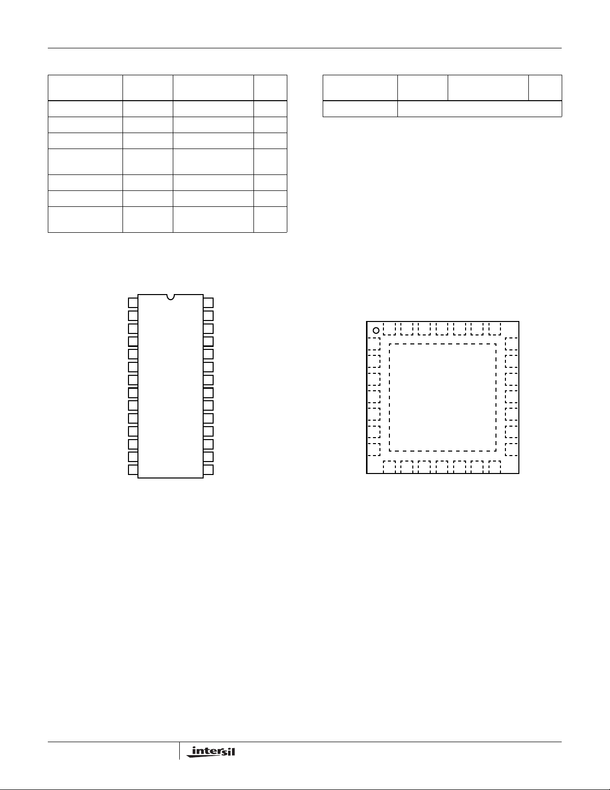
Ordering Information
PART
NUMBER
ISL6551IB 0 to 85 28 Ld SOIC M28.3
ISL6551IBZ (Note) 0 to 85 28 Ld SOIC (Pb-free) M28.3
ISL6551IR 0 to 85 28 Ld 6x6 QFN L28.6x6
ISL6551IRZ (Note) 0 to 85 28 Ld 6x6 QFN
ISL6551ABZ (Note) -40 to 105 28 Ld SOIC (Pb-free) M28.3
ISL6551AR -40 to 105 28 Ld 6x6 QFN L28.6x6
ISL6551ARZ (Note) -40 to 105 28 Ld 6x6 QFN
TEMP
RANGE (°C) PACKAGE
(Pb-free)
(Pb-free)
PKG.
DWG. #
L28.6x6
L28.6x6
Pinouts
28 PIN WIDE BODY (SOIC)
TOP VIEW
VDD
VSS
CT
RD
R_RESDLY
R_RA
ISENSE
PKILIM
BGREF
R_LEB
CS_COMP
CSS
EANI
EAI
EAO
1
2
3
4
5
6
7
8
9
10
11
12
13
14
28
27
26
25
24
23
22
21
20
19
18
17
16
15
VDDP1
VDDP2
PGND
UPPER1
UPPER2
LOWER1
LOWER2
SYNC1
SYNC2
ON/OFF
DCOK
LATSD
SHARE
Ordering Information (Continued)
PART
NUMBER
ISL6551EVAL1 Evaluation Platform (ISL6551IR only)
Add “-T” suffix for tape and reel.
NOTE: Intersil Pb-free plus anneal products employ special Pb-free
material sets; molding compounds/die attach materials and 100%
matte tin plate termination finish, which are RoHS compliant and
compatible with both SnPb and Pb-free soldering operations.
Intersil Pb-free products are MSL classified at Pb-free peak reflow
temperatures that meet or exceed the Pb-free requirements of
IPC/JEDEC J STD-020.
R_RESDLY
ISENSE
PKILIM
BGREF
R_LEB
CS_COMP
R_RA
1
2
3
4
5
6
7
TEMP
RANGE (°C) PACKAGE
28 PIN (QFN)
TOP VIEW
RD
CT
VSS
VDD
VDDP1
VDDP2
28 27 26 25 24 23 22
8 9 10 11 12 13 14
EANI
EAI
EAO
LATSD
SHARE
CSS
PGND
21
20
19
18
17
16
15
DCOK
PKG.
DWG. #
UPPER1
UPPER2
LOWER1
LOWER2
SYNC1
SYNC2
ON/OFF
2
FN9066.5
January 3, 2006
Page 3

ISL6551
www.BDTIC.com/Intersil
Functional Pin Description
PACKAGE PIN #
PIN SYMBOL FUNCTIONSOIC QFN
1 26 VSS Reference ground. All control circuits are referenced to this pin.
2 27 CT Set the oscillator frequency, up to 1MHz.
3 28 RD Adjust the clock dead time from 50ns to 1000ns.
4 1 R_RESDLY Program the resonant delay from 50ns to 500ns.
5 2 R_RA Adjust the ramp for slope compensation (from 50mV to 250mV).
6 3 ISENSE The pin receives the current information via a current sense transformer or a power resistor.
7 4 PKILIM Set the over current limit with the bandgap reference as the trip threshold.
8 5 BGREF Precision bandgap reference, 1.263V ±2% overall recommended operating conditions.
9 6 R_LEB Program the leading edge blanking from 50ns to 300ns.
10 7 CS_COMP Set a low current sharing loop bandwidth with a capacitor.
11 8 CSS Program the rise time and the clamping voltage with a capacitor and a resistor, respectively.
12 9 EANI Non-inverting input of Error Amp. It is clamped by the voltage at the CSS pin (Vclamp).
13 10 EAI Inverting input of Error Amp. It receives the feedback voltage.
14 11 EAO Output of Error Amp. It is clamped by the voltage at the CSS pin (Vclamp).
15 12 SHARE This pin is the SHARE BUS connecting with other unit(s) for current share operation.
16 13 LATSD The IC is latched off with a voltage greater than 3V at this pin and is reset by recycling VDD.
17 14 DCOK Power Good indication with a ±5% window.
18 15 ON/OFF This is an Enable pin that controls the states of all drive signals and the soft-start.
19, 20 16, 17 SYNC2, SYNC1 These are the gate control signals for the output synchronous rectifiers.
21, 22 18, 19 LOWER2, LOWER1 Both lower drivers are PWM-controlled on the trailing edge.
23, 24 20, 21 UPPER2, UPPER1 Both upper drivers are driven at a fixed 50% duty cycle.
25 22 PGND Power Ground. High current return paths for both the upper and the lower drivers.
26, 27 23, 24 VDDP2, VDDP1 Power is delivered to both the upper and the lower drivers through these pins.
28 25 VDD Power is delivered to all control circuits including SYNC1 & SYNC2 via this pin.
3
FN9066.5
January 3, 2006
Page 4
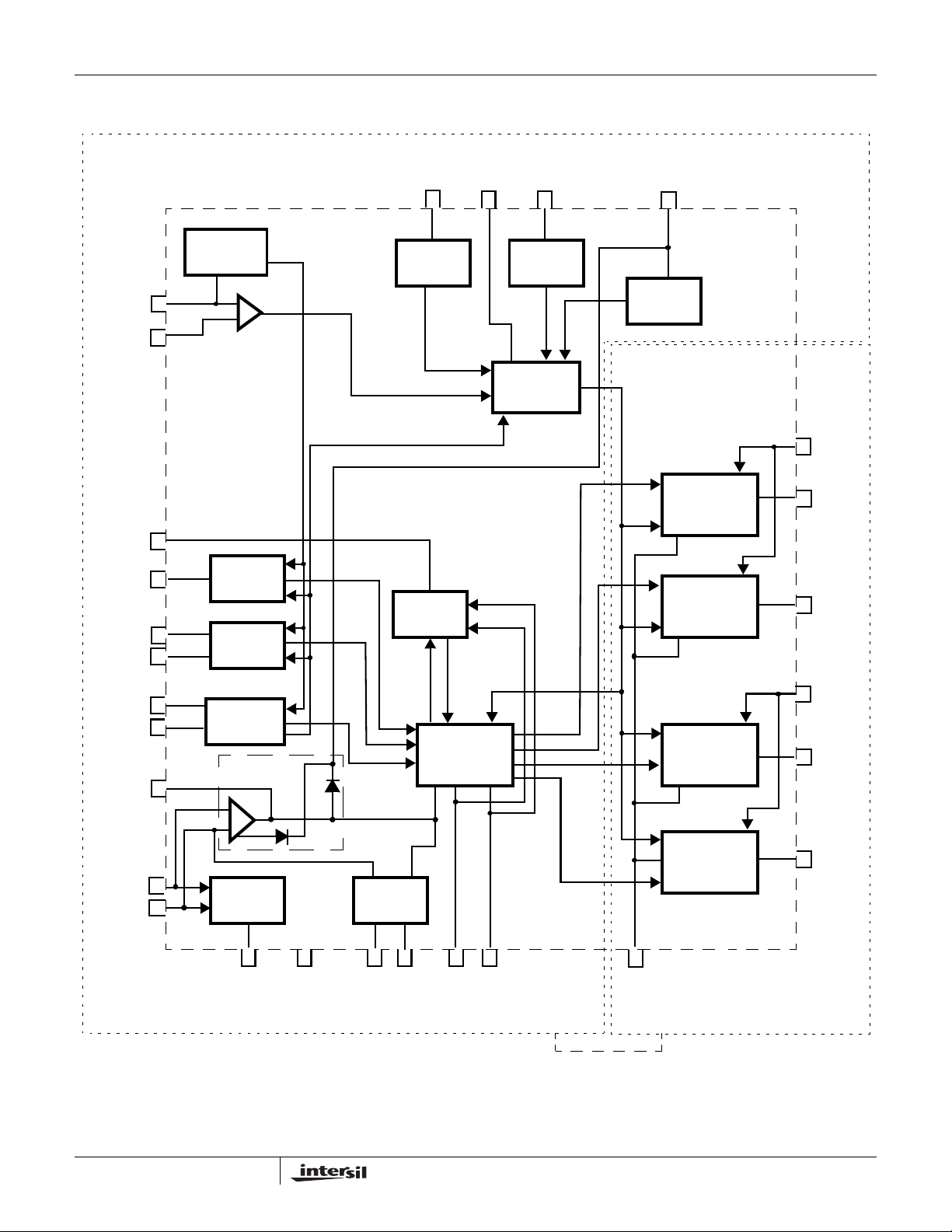
Functional Block Diagram
www.BDTIC.com/Intersil
ISL6551
BGREF
PKILIM
R_LEB
R_RESDLY
ISENSE
R_RA
8
7
9
4
6
5
BANDGAP
REFERENCE
RESODLY
RESODLY
RAMP
RAMP
ADJUST
ADJUST
VDD
28
UVLO
LEB
ON/OFF
18
SHUTDOWN
SHUTDOWN
LATCH
SHUTDOWN
SHUTDOWN
LATSD
16
LATCH
SOFT
SOFT-
START
START
CSS
11
UPPER1
DRIVER
UPPER2
DRIVER
27
24
23
VDDP1
UPPER1
UPPER2
2
CT
3
RD
EAO
14
13
EAI
12
EANI
CIRCUITS REFERENCED TO VSS
CLOCK
GENERATOR
ERROR AMP
(See Fig. 4)
DC OK
17
DCOK
1
VSS
CURRENT
SHARE
10
15
CS_COMP
SHARE
PWM
LOGIC
20
19
SYNC2
SYNC1
EXTERNAL SINGLE POINT CONNECTION REQUIRED
25
PGND
CIRCUITS REFERENCED TO PGND
LOWER1
DRIVER
LOWER2
DRIVER
26
22
21
VDDP2
LOWER1
LOWER2
4
FN9066.5
January 3, 2006
Page 5
ISL6551
www.BDTIC.com/Intersil
Absolute Maximum Ratings Thermal Information
Supply Voltage VDD, VDDP1, VDDP2 . . . . . . . . . . . . . . -0.3 to 16V
Enable Inputs (ON/OFF, LATSD) . . . . . . . . . . . . . . . . . . . . . . . . VDD
Power Good Sink Current (I
ESD Rating
Human Body Model (Per MIL-STD-883 Method 3015.7) . . . . .3kV
Machine Model (Per EIAJ ED-4701 Method C-111). . . . . . . . 250V
) . . . . . . . . . . . . . . . . . . . . . . 5mA
DCOK
Thermal Resistance θ
QFN Package (Notes 1, 3). . . . . . . . . . 30 2.5
SOIC Package (Note 2) . . . . . . . . . . . . 55 N/A
Maximum Junction Temperature (Plastic Package) . . . . . . . . 150°C
Maximum Storage Temperature Range. . . . . . . . . . . -65°C to 150°C
Maximum Lead Temperature (Soldering 10s) . . . . . . . . . . . . . 300°C
(SOIC Lead Tips Only)
Recommended Operating Conditions
Ambient Temperature Range
ISL6551IB . . . . . . . . . . . . . . . . . . . . . . . . . . . . . . . . . . . 0°C to 85°C
ISL6551AB. . . . . . . . . . . . . . . . . . . . . . . . . . . . . . . . . -40°C to 105°C
Supply Voltage Range, VDD . . . . . . . . . . . . . . . . . . . 10.8V to 13.2V
Supply Voltage Range, VDDP1 & VDDP2. . . . . . . . . . . . . . . <13.2V
Maximum Operating Junction Temperature. . . . . . . . . . . . . . . 125°C
CAUTION: Stresses above those listed in “Absolute Maximum Ratings” may cause permanent damage to the device. This is a stress only rating and operation of the
device at these or any other conditions above those indicated in the operational sections of this specification is not implied.
NOTES:
1. θ
is measured in free air with the component mounted on a high effective thermal conductivity test board with “direct attach” features. See
JA
Tech Brief TB379 for details.
is measured with the component mounted on a high effective thermal conductivity test board in free air. See Tech Brief TB379 for details.
2. θ
JA
3. For θ
, the “case temp” location is the center of the exposed metal pad on the package underside.
JC
(°C/W) θJC (°C/W)
JA
Electrical Specifications These specifications apply for VDD = VDDP = 12V and T
(ISL6551AB), Unless Otherwise Stated
PARAMETER SYMBOL TEST CONDITIONS MIN TYP MAX UNITS
SUPPLY (VDD, VDDP1, VDDP2)
Supply Voltage VDD 10.8 12.0 13.2 V
Bias Current from VDD (ISL6551IB) IDD VDD = 12V (not including drivers current at VDDP) 5 13 18 mA
Bias Current from VDD (ISL6551AB) IDD VDD = 12V (not including drivers current at VDDP) 3 20 mA
Total Current from VDD and VDDP ICC VDD = VDDP = 12V, F = 1MHz, 1.6nF Load 60 mA
UNDER VOLTAGE LOCKOUT (UVLO)
Start Threshold (ISL6551IB) VDD
Start Threshold (ISL6551AB) VDD
Stop Threshold (ISL6551IB) VDD
Stop Threshold (ISL6551AB) VDD
Hysteresis (ISL6551IB) VDD
Hysteresis (ISL6551AB) VDD
CLOCK GENERATOR (CT, RD)
Frequency Range F VDD = 12V (Figure 2) 100 1000 kHz
Dead Time Pulse Width (Note 4) DT VDD = 12V (Figure 3) 50 1000 ns
BANDGAP REFERENCE (BGREF)
Bandgap Reference Voltage
(ISL6551IB)
Bandgap Reference Voltage
(ISL6551AB)
Bandgap Reference Output Current IREF VDD = 12V, see Block/Pin Functional Descriptions
ON
ON
OFF
OFF
HYS
HYS
VREF VDD = 12V, 399kΩ pull-up, 0.1µF, after trimming 1.250 1.263 1.280 V
VREF VDD = 12V, 399kΩ pull-up, 0.1µF, after trimming 1.244 1.263 1.287 V
for details
= 0°C to 85°C (ISL6551IB) or -40°C to 105°C
A
9.2 9.6 9.9 V
9.16 9.94 V
8.03 8.6 8.87 V
7.98 8.92 V
0.3 1 1.9 V
0.27 1.93 V
100 µA
5
FN9066.5
January 3, 2006
Page 6

ISL6551
www.BDTIC.com/Intersil
Electrical Specifications These specifications apply for VDD = VDDP = 12V and T
(ISL6551AB), Unless Otherwise Stated (Continued)
PARAMETER SYMBOL TEST CONDITIONS MIN TYP MAX UNITS
PWM DELAYS (Note 4)
LOW1,2 delay “Rising” LOWR With respect to RESDLY rising 5 ns
LOW1,2 delay “Falling” LOWF Compare Delay @ Verror = Vramp 44 ns
SYNC1,2 delay “Falling” SYNCF With respect to RESDLY falling and with 20pF load 18 ns
SYNC1,2 delay “Rising” SYNCR With respect to CLK rising and with 20pF load 20 ns
ERROR AMPLIFIER (EANI, EAI, EAO) (Note 4)
Unity Gain Bandwidth UGBW 10 MHz
DC Gain DCG 79 dB
Maximum Offset Error Voltage Vos 3.1 mV
Input Common Mode Range Vcm VDD = 12V 0.4 9 V
Common Mode Rejection Ratio CMMR 82 dB
Power Supply Rejection Ratio PSSR 1mA load 95 dB
Maximum Output Source Current ISRC 2 mA
Maximum Lower Saturation Voltage Vsatlow Sinking 0.27mA 125 mV
RAMP ADJUST (R_RA) (Note 4)
Ramp Frequency F 100 1000 kHz
Linear Voltage Ramp, Minimum LVR 50 mV
Linear Voltage Ramp, Maximum 250 mV
Overall Variation 25 %
PEAK CURRENT LIMIT (PKILIM)
Peak Current Shutdown Threshold IpkThr BGREF = 0.1µF, 399kΩ pull-up 1.25 1.263 1.31 V
Peak Current Shutdown Delay
(Note 4)
SOFT-START (CSS)
Charge Current Iss Vcss = 0.6V 8 12 µA
Discharge Current Idis 1.6 5.2 mA
Cycle-by-Cycle Current Limit
(ISL6551IB)
Cycle-by-Cycle Current Limit
(ISL6551AB)
DRIVERS (UPPER1, UPPER2, LOWER1, LOWER2)
Maximum Capacitive Load (each) CL VDD = VDDP = 12V, F = 1MHz,
Turn On Rise Time (ISL6551IB) Tr 1.0nF Capacitive load 8.9 16 ns
Turn On Rise Time (ISL6551AB) Tr 1.0nF Capacitive load 9.2 17 ns
Turn Off Fall Time (ISL6551IB) Tf 1.0nF Capacitive load 6.4 10 ns
Turn Off Fall Time (ISL6551AB) Tf 1.0nF Capacitive load 12 ns
Shutdown Delay (Note 4) T
Rising Edge Delay (Note 4) T
Falling Edge Delay (Note 4) T
Vsat_sourcing Vsat_high Sourcing 20mA 1.00 V
IpkDel 75 ns
Vclamp 2 8 V
Vclamp 1.9 8.1 V
Thermal Dependence
SD
RD
FD
1.0nF Capacitive load 14.5 ns
1.0nF Capacitive load 16.4 ns
1.0nF Capacitive load 13.7 ns
Sourcing 200mA 1.35 V
= 0°C to 85°C (ISL6551IB) or -40°C to 105°C
A
1600 pF
6
FN9066.5
January 3, 2006
Page 7

ISL6551
www.BDTIC.com/Intersil
Electrical Specifications These specifications apply for VDD = VDDP = 12V and T
(ISL6551AB), Unless Otherwise Stated (Continued)
PARAMETER SYMBOL TEST CONDITIONS MIN TYP MAX UNITS
Vsat_sinking (ISL6551IB) Vsat_low Sinking 20mA 0.035 V
Sinking 200mA 0.31 V
Vsat_sinking (ISL6551AB) Vsat_low Sinking 20mA 0.04 V
Sinking 200mA 0.5 V
SYNCHRONOUS SIGNALS (SYNC1, SYNC2)
Maximum capacitive load (each) VDD = 12, F = 1MHz 20 pF
PROGRAMMABLE DELAYS (RESDLY, LEB) (Note 4)
Resonant Delay Adjust Range (Figure 7) 50 500 ns
Resonant Delay t
Leading Edge Blanking Adjust
Range
Leading Edge Blanking t
LATCHING SHUTDOWN (LATSD)
Fault Threshold VIN 3 V
Fault_NOT Threshold VINN 1.9 V
Time to Set latch (Note 4) TSET 415 ns
ON/OFF (ONOFF)
Turn-off Threshold OFF 0.8 V
Turn-on Threshold ON 2 V
CURRENT SHARE (SHARE, CS_COMP) (Note 4)
Voltage Offset Between Error Amp
Voltage of Master and Slave
Maximum Source Current To
External Reference
Maximum Correctable Deviation In
Reference Voltage Between Master
and Slave
Share/Adjust Loop Bandwidth CS BW CS_COMP = 0.1µF 500 Hz
DC OK (DCOK)
Sink Current I
Saturation Voltage V
Input Reference Vref_in 1 5 V
Threshold (relative to Vref_in) OV (Figure 11) 5 %
Recovery (relative to Vref_in) OV (Figure 11) 3 %
Threshold (relative to Vref_in) UV (Figure 11) -5 %
Recovery (relative to Vref_in) UV (Figure 11) -3 %
Transient Rejection (Note 4) TRej 100mV transient on Vout (system implicit rejection
NOTE:
4. Guaranteed by design. Not 100% tested in production.
RESDLY
LEB
Vcs_offset SHARE = 30K 30 mV
Ics_source SHARE = 30K 190 µA
DCOK
SATDCOKIDCOK
R_RESDLY = 10K 55 ns
R_RESDLY = 120K 488 ns
(Figure 8) 50 300 ns
R_LEB = 20K 64 ns
R_LEB = 140K 302 ns
R_LEB = 12V 0 ns
SHARE = 30K, Rsource = 1K,
OUTPUT REFERENCE = 1 to 5V,
(See Figure 10)
= 5mA 0.4 V
and feedback network dependence (Figure 12)
= 0°C to 85°C (ISL6551IB) or -40°C to 105°C
A
190 mV
5mA
250 µs
7
FN9066.5
January 3, 2006
Page 8
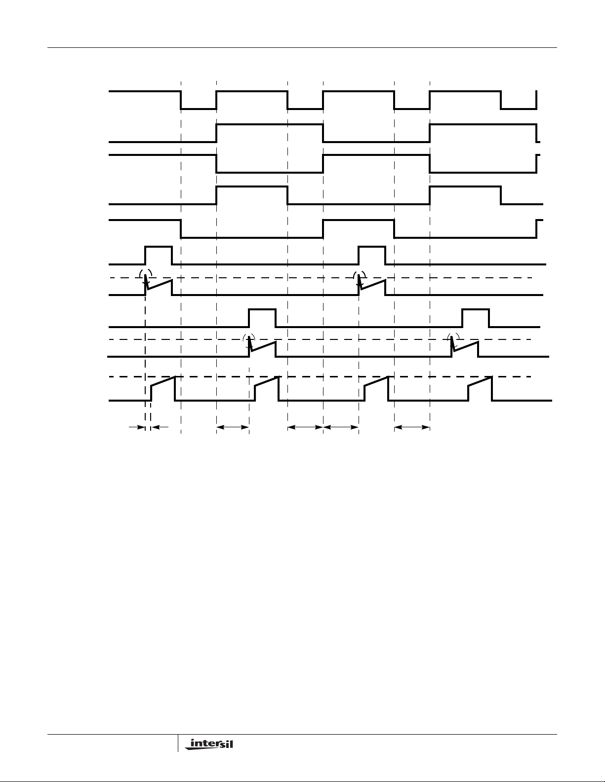
Drive Signals Timing Diagrams
www.BDTIC.com/Intersil
CLOCK
UPPER1
UPPER2
SYNC1
SYNC2
LOWER1
I
LOWER1
ISL6551
EAO
LOWER2
I
LOWER2
RAMP ADJUST
OUTPUT TO
PWM
LOGIC
T1
NOTES:
T1 = Leading edge blanking
T2 = T4 = Resonant delay
T3 = T5 = dead time
In the above figure, the values for T1 through T5 are exaggerated for demonstration purposes.
T2 T3 T4 T5
Timing Diagram Descriptions
The two upper drivers (UPPER1 and UPPER2) are driven at
a fixed 50% duty cycle and the two lower drivers (LOWER1
and LOWER2) are PWM-controlled on the trailing edge,
while the leading edge employs resonant delay (T2 and T4).
In current mode control, the sensed switch (FET) current
(I
LOWER1
and I
LOWER2
) is processed in the Ramp Adjust
and Leading Edge Blanking (LEB) circuits and then compared
to a control signal (EAO). Spikes, due to parasitic elements in
the bridge circuit, would falsely trigger the comparator
generating the PWM signal. To prevent false triggering, the
leading edge of the sensed current signal is blanked out by
T1, which can be programmed at the R_LEB pin with a
resistor. Internal switches gate the analog input to the PWM
comparator, implementing the blanking function that
eliminates response degrading delays which would be caused
if filtering of the current feedback was incorporated. The dead
time (T3 and T5) is the delay to turn on the upper FET
(UPPER1/UPPER2) after its corresponding lower FET
(LOWER1/LOWER2) is turned off when the bridge is
operating at maximum duty cycle in normal conditions, or is
responding to load transients or input line dipping conditions.
Therefore, the upper and lower FETs that are located at the
same side of the bridge can never be turned on together, which
eliminates shoot-through currents. SYNC1 and SYNC2 are the
gate control signals for the output synchronous rectifiers. They
are biased by VDD and are capable of driving capacitive loads
up to 20pF at 1MHz clock frequency (500kHz switching
frequency). External drivers with high current capabilities are
required to drive the synchronous rectifiers, cascading with
both synchronous signals (SYNC1 and SYNC2).
EAO
EAO
8
FN9066.5
January 3, 2006
Page 9

Shutdown Timing Diagrams
www.BDTIC.com/Intersil
ISL6551
LATSD
ON/OFF
VDD
ILIM_OUT
SOFT
START
DRIVER
ENABLE
SOFT-START
SHUTDOWN
A
FAULT
> BGREF
PKILIM
PKILIM < BGREF
C
B
LATCH CANNOT BE RESET BY ON/OFF
D
E
VDD
ON
LATCH RESET BY
REMOVING VDD
FAULT
F
VDD
OFF
OFF
OVER
CURRENT
Shutdown Timing Descriptions
A (ON/OFF) - When the ON/OFF is pulled low, the soft-start
capacitor is discharged and all the drivers are disabled.
When the ON/OFF is released without a fault condition, a
soft-start is initiated.
B (OVERCURRENT) - If the output of the converter is over
loaded, i.e., the PKILIM is above the bandgap reference
voltage (BGREF), the soft-start capacitor is discharged very
quickly and all the drivers are turned off. Thereafter, the softstart capacitor is charged slowly, and discharged quickly if
the output is overloaded again. The soft-start will remain in
hiccup mode as long as the overload conditions persist.
Once the overload is removed, the soft-start capacitor is
charged up and the converter is then back to normal
operation.
C (LATCHING SHUTDOWN) - The IC is latched off
completely as the LATSD pin is pulled high, and the soft-start
capacitor is reset.
D (ON/OFF) - The latch cannot be reset by the ON/OFF.
LATCHED OFF/ON
E (LATCH RESET) - The latch is reset by removing the
VDD. The soft-start capacitor starts to be charged after VDD
increases above the turn-on threshold VDD
F (VDD UVLO) - The IC is turned off when the VDD is below
the turn-off threshold VDD
incorporated in the undervoltage lockout (UVLO) circuit.
LATCH
RESET
UNDER VOLTAGE
LOCKOUT
. Hysteresis VDD
OFF
ON
.
HYS
is
9
FN9066.5
January 3, 2006
Page 10

ISL6551
www.BDTIC.com/Intersil
Block/Pin Functional Descriptions
Detailed descriptions of each individual block in the functional
block diagram on page 3 are included in this section.
Application information and design considerations for each pin
and/or each block are also included.
• IC Bias Power (VDD, VDDP1, VDDP2)
- The IC is powered from a 12V
- VDD supplies power to both the digital and analog circuits
and should be bypassed directly to the VSS pin with an
0.1µF low ESR ceramic capacitor.
- VDDP1 and VDDP2 are the bias supplies for the upper
drivers and the lower drivers, respectively. They should be
decoupled with ceramic capacitors to the PGND pin.
- Heavy copper should be attached to these pins for a better
heat spreading.
• IC GNDs (VSS, PGND)
- VSS is the reference ground, the return of VDD, of all
control circuits and must be kept away from nodes with
switching noises. It should be connected to the PGND in
only one location as close to the IC as practical. For a
secondary side control system, it should be connected to
the net after the output capacitors, i.e., the output return
pinout(s). For a primary side control system, it should be
connected to the net before the input capacitors, i.e., the
input return pinout(s).
- PGND is the power return, the high-current return path of
both VDDP1 and VDDP2. It should be connected to the
SOURCE pins of two lower power switches or the
RETURNs of external drivers as close as possible with
heavy copper traces.
- Copper planes should be attached to both pins.
± 10% supply.
• Undervoltage Lockout (UVLO)
- UVLO establishes an orderly start-up and verifies that VDD
is above the turn-on threshold voltage (VDD
). All the
ON
drivers are held low during the lockout. UVLO incorporates
hysteresis VDD
to prevent multiple startup/shutdowns
HYS
while powering up.
- UVLO limits are not applicable to VDDP1 and VDDP2.
• Bandgap Reference (BGREF)
- The reference voltage VREF is generated by a precision
bandgap circuit.
- This pin must be pulled up to VDD with a resistance of
approximately 399kΩ for proper operation. For additional
reference loads (no more than 1mA), this pull-up resistor
should be scaled accordingly.
- This pin must also be decoupled with an 0.1µF low ESR
ceramic capacitor.
• Clock Generator (CT, RD)
- This free-running oscillator is set by two external
components as shown in Figure 1. A capacitor at CT is
charged and discharged with two equal constant current
sources and fed into a window comparator to set the clock
frequency. A resistor at RD sets the clock dead time. RD
and CT should be tied to the VSS pin on their other ends
as close as possible. The corresponding CT for a particular
frequency can be selected from Figure 2.
- The switching frequency (Fsw) of the power train is half of
the clock frequency (Fclock), as shown in Equation 1.
Fsw
Fclock
-------------------=
2
(EQ. 1)
RD
CT
CT
RD
I_CT
I_CT
10
SET CLOCK
DEAD TIME (DT)
-
VDD
VMAX
VMIN
FIGURE 1. SIMPLIFIED CLOCK GENERATOR CIRCUIT
OUT
+
S
OUT
+
Q
Q
R
CLK
Q
Q
CLK
DT
DT
January 3, 2006
FN9066.5
Page 11

ISL6551
www.BDTIC.com/Intersil
3,000
0°C
60°C
2,500
120°C
2,000
1,500
F (kHz)
1,000
500
0
10
FIGURE 2. CT vs FREQUENCY
100 10,000
CT (pF)
RECOMMENDED RANGE
1,000
- Note that the capacitance of a scope probe (~12pF for
single ended) would induce a smaller frequency at the
CT pin. It can be easily seen at a higher frequency. An
accurate operating frequency can be measured at the
outputs of the bridge/synchronous drivers.
- The dead time is the delay to turn on the upper FET
(UPPER1/UPPER2) after its corresponding lower FET
(LOWER1/LOWER2) is turned off when the bridge is
operating at maximum duty cycle in normal conditions,
or is responding to load transients or input line dipping
conditions. This helps to prevent shoot through between
the upper FET and the lower FET that are located at the
same side of the bridge. The dead time can be
estimated using Equation 2:
DT
MRD×
--------------------=
kΩ
(ns)
(EQ. 2)
where M=11.4(VDD=12V), 11.1(VDD=14V), and
12(VDD=10V), and RD is in kΩ. This relationship is
shown in Figure 3.
2
1.6
1.2
0.8
DEAD TIME (µs)
0.4
0
20 40 60 80 100 120 140 160
0
RD (kΩ)
FIGURE 3. RD vs DEAD TIME (VDD = 12V)
• Error Amplifier (EAI, EANI, EAO)
- This amplifier compares the feedback signal received at
the EAI pin to a reference signal set at the EANI pin and
provides an error signal (EAO) to the PWM Logic. The
feedback loop compensation can be programmed via
these pins.
- Both EANI and EAO are clamped by the voltage
(Vclamp) set at the CSS pin, as shown in Figure 4. Note
that the diodes in the functional block diagram represent
the clamp function of the CSS in a simplified way.
• Soft-Start (CSS)
- The voltage on an external capacitor charged by an
internal current source I
is fed into a control pin on
SS
the error amplifier. This causes the Error Amplifier to: 1)
limit the EAO to the soft-start voltage level; and 2) override the reference signal at the EANI with the soft-start
voltage, when the EANI voltage is higher than the softstart voltage. Thus, both the output voltage and current
of the power supply can be controlled by the soft-start.
- The clamping voltage determines the cycle-by-cycle
peak current limiting of the power supply. It should be
set above the EANI and EAO voltages and can be
programmed by an external resistor as shown in
Figure 4 using Equation 3.
Vclamp Rcss Iss•=
(See Fig. 9)
SSL
(TO
BLANKING
CIRCUIT)
ERROR AMP
CSS
R
CSS
Iss
SHUTDOWN
400mV
VDD
FIGURE 4. SIMPLIFIED CLAMP/SOFT-START
+
-
11
(V)
EAI
(–)
EANI
(+)
EAO
(EQ. 3)
FN9066.5
January 3, 2006
Page 12

ISL6551
www.BDTIC.com/Intersil
- Per Equation 3, the clamping voltage is a function of the
charge current Iss. For a more predictable clamping
voltage, the CSS pin can be connected to a referencebased clamp circuit as shown in Figure 5. To make the
Vclamp less dependent on the soft-start current (Iss),
the currents flowing through R1 and R2 should be
scaled much greater than Iss. The relationship of this
circuit can be found in Equation 4.
V
REF
R1
CSS
R2
FIGURE 5. REFERENCE-BASED CLAMP CIRCUIT
R1 R2×
Vclamp Iss
----------------------
• Vref
R1 R2+
- The soft-start rise time (T
Equation 5. The rise time (T
ss
R2
----------------------
•+≈
R1 R2+
(EQ. 4)
) can be calculated with
) of the output voltage is
rise
approximated with Equation 6.
T
T
ss
rise
Vclamp Css×
---------------------------------------=
Iss
EANI Css×
--------------------------------=
Iss
(s)
(s)
(EQ. 5)
(EQ. 6)
• Drivers (Upper1, Upper2, Lower1, Lower2)
- The two upper drivers are driven at a fixed 50% duty
cycle and the two lower drivers are PWM-controlled on
the trailing edge while the leading edge employs resonant
delay. They are biased by VDDP1 and VDDP2,
respectively.
- Each driver is capable of driving capacitive loads up to CL
at 1MHz clock frequency and higher loads at lower
frequencies on a layout with high effective thermal
conductivity.
- The UVLO holds all the drivers low until the VDD has
reached the turn-on threshold VDD
ON
.
- The upper drivers require assistance of external levelshifting circuits such as Intersil’s HIP2100 or pulse
transformers to drive the upper power switches of a bridge
converter.
• Peak Current Limit (PKILIM)
- When the voltage at PKILIM exceeds the BGREF voltage,
the gate pulses are terminated and held low until the next
clock cycle. The peak current limit circuit has a high-speed
loop with propagation delay IpkDel. Peak current
shutdown initiates a soft-start sequence.
- The peak current shutdown threshold is usually set slightly
higher than the normal cycle-by-cycle PWM peak current
limit (Vclamp) and therefore will normally only be activated
in a short-circuit condition. The limit can be set with a
resistor divider from the ISENSE pin. The resistor divider
relationship is defined in Equation 7.
- In general, the trip point is a little smaller than the BGREF
due to the noise and/or ripple at the BGREF.
R
UP
R
DOWN
FIGURE 6. PEAK CURRENT LIMIT SET CIRCUIT
Rdown
-------------------------------------Rdown Rup+
BGREF
-----------------------------------------=
ISENSE max()
ISENSE
PKILIM
(EQ. 7)
• Latching Shutdown (LATSD)
- A high TTL level on LATSD latches the IC off. The IC goes
into a low power mode and is reset only after the power at
the VDD pin is removed completely. The ON/OFF cannot
reset the latch.
- This pin can be used to latch the power supply off on
output overvoltage or other undesired conditions.
• ON/OFF (ON/OFF)
- A high standard TTL input (safe also for VDD level) signals
the controller to turn on. A low TTL input turns off the
controller and terminates all drive signals including the
SYNC outputs. The soft-start is reset.
- This pin is a non-latching input and can accept an enable
command when monitoring the input voltage and the
thermal condition of a converter.
• Resonant Delay (R_RESDLY)
- A resistor tied between R_RESDLY and VSS determines
the delay that is required to turn on a lower FET after its
corresponding upper FET is turned off. This is the resonant
delay, which can be estimated with Equation 8.
t
RESDLY
= 4.01 x R_RESDLY/kΩ + 13 (ns)
(EQ. 8)
- Figure 7 illustrates the relationship of the value of the
resistor (R_RESDLY) and the resonant delay (t
RESDLY
The percentages in the figure are the tolerances at the two
end points of the curve.
).
12
FN9066.5
January 3, 2006
Page 13

ISL6551
www.BDTIC.com/Intersil
500
450
400
350
(ns)
300
250
RESDLY
t
200
150
+37%
100
50
0 20 40 60 80 100 120
+4%
R_RESDLY (kΩ)
+18%
-24%
FIGURE 7. R_RESDLY vs RESDLY
• Leading Edge Blanking (R_LEB)
- In current mode control, the sensed switch (FET) current is
processed in the Ramp Adjust and LEB circuits and then
compared to a control signal (EAO voltage). Spikes, due to
parasitic elements in the bridge circuit, would falsely trigger
the comparator generating the PWM signal. To prevent
false triggering, the leading edge of the sensed current
signal is blanked out by a period that can be programmed
with the R_LEB resistor. Internal switches gate the analog
input to the PWM comparator, implementing the blanking
function that eliminates response degrading delays which
would be caused if filtering of the current feedback was
incorporated. The current ramp is blanked out during the
resonant delay period because no switching occurs in the
lower FETs. The leading edge blanking function will not be
activated until the soft-start (CSS) reaches over 400mV, as
illustrated in Figures 4 and 9. The leading edge blanking
(LEB) function can be disabled by tying the R_LEB pin to
VDD, i.e., LEB=1. Never leave the pin floating.
- The blanking time can be estimated with Equation 9,
whose relationship can be seen in Figure 8. The
percentages in the figure are the tolerances at the two
endpoints of the curve.
= 2 x R_LEB / kΩ + 15 (ns)
t
LEB
300
250
200
(ns)
150
LEB
t
+51%
100
-11%
50
0
20 40 60 80 100 120 140
R_LEB (kΩ)
FIGURE 8. R_LEB vs t
LEB
(EQ. 9)
+20%
-18%
399K
0.1µ
R_RA
R_LEB
R_RA
ISENSE
R_LEB
VDD
BGREF
ADD RAMP
ADJ_RAMP
200mV
RAMP_OUT
(TO PWM
COMPARATOR)
+
-
200mV
200mV
RESDLY LEB SSL RAMP_OUT
ADJ_RAMP
0
RAMP_OUT
ISENSE
0XXBLANK
SET
BLANKING
TIME
RESDLY
LEB
SSL
(See Fig. 4)
X00BLANK
1 1 X NO BLANK
1 X 1 NO BLANK
FIGURE 9. SIMPLIFIED RAMP ADJUST AND LEADING EDGE BLANKING CIRCUITS
BLANK
13
FN9066.5
January 3, 2006
Page 14

ISL6551
www.BDTIC.com/Intersil
• Ramp Adjust (R_RA, ISENSE)
- The ramp adjust block adds an offset component
(200mV) and a slope adjust component to the ISENSE
signal before processing it at the PWM Logic block, as
shown in Figure 9. This ensures that the ramp voltage is
always higher than the OAGS (ground sensing opamp)
minimum voltage to achieve a “zero” state.
- It is critical that the input signal to ISENSE decays to
zero prior to or during the clock dead time. The levelshifting and capacitive summing circuits in the RAMP
ADJUST block are reset during the dead time. Any input
signal transitions that occur after the rising edge of CLK
and prior to the rising edge of RESDLY can cause
severe errors in the signal reaching the PWM
comparator.
- Typical ramp values are hundreds of mV over the period
on a 3V full scale current. Too much ramp makes the
controller look like a voltage mode PWM, and too little
ramp leads to noise issues (jitter). The amount of ramp
(Vramp), as shown in Figure 9, is programmed with the
R_RA resistor and can be calculated with Equation 10.
V
= BGREF x dt /(R_RA x 500E-12) (V)
ramp
where dt = Duty Cycle / Fsw - t
(s). Duty cycle is
LEB
(EQ. 10)
discussed in detail in application note AN1002.
- The voltage representation of the current flowing
through the power train at ISENSE pin is normally
scaled such that the desired peak current is less than or
equal to Vclamp-200mV-Vramp, where the clamping
voltage is set at the CSS pin.
• SYNC Outputs (SYNC1, SYNC2)
- SYNC1 and SYNC2 are the gate control signals for the
output synchronous rectifiers. They are biased by VDD
and are capable of driving capacitive loads up to 20pF
at 1MHz clock frequency (500kHz switching frequency).
These outputs are turned off sooner than the turn-off at
UPPER1 and UPPER2 by the clock dead time, DT.
- Inverting both SYNC signals or both LOWER signals is
another possible way to control the drivers of the
synchronous rectifiers. When using these drive
schemes, the user should understand the issues that
might occur in his/her applications, especially the
impacts on current share operation and light load
operation. Refer to application note AN1002 for more
details.
- External high current drivers controlled by the
synchronous signals are required to drive the
synchronous rectifiers. A pulse transformer is required
to pass the drive signals to the secondary side if the IC
is used in a primary control system.
• Share Support (SHARE, CS_COMP)
- The unit with the highest reference is the master. Other
units, as slaves, adjust their references via a source
resistor to match the master reference sharing the load
current. The source resistor is typically 1kΩ connecting
the EANI pin and the OUTPUT REFERENCE (external
reference or BGREF), as shown in Figure 10. The share
bus represents a 30kΩ resistive load per unit, up to 10
units.
- The output (ADJ) of “Operational Transconductance
Amplifier (OTA)” can only pull high and it is floating while
in master mode. This ensures that no current is sourced
to the OUTPUT REFERENCE when the IC is working
by itself.
- The slave units attempt to drive their error amplifier
voltage to be within a pre-determined offset (30mV
typical) of the master error voltage (the share bus). The
current-share error is nominally (30mV/EAO)*100%
assuming no other source of error. With a 2.5V full load
error amp voltage, the current-share error at full load
would be -1.2% (slaves relative to master).
- The bandwidth of the current sharing loop should be
much lower than that of the voltage loop to eliminate
noise pick-up and interactions between the voltage
regulation loop and the current loop. A 0.1µF capacitor
is recommended between CS_COMP and VSS pins to
achieve a low current sharing loop bandwidth (100Hz to
500Hz).
30mV
+
EAO
+
-
FIGURE 10. SIMPLIFIED CURRENT SHARE CIRCUIT
-
+
OTA
ADJ
14
CS_COMP
0.1µF
EANI
(+)
SHARE
30K
1K
OUTPUT
REFERENCE
FN9066.5
January 3, 2006
Page 15

ISL6551
www.BDTIC.com/Intersil
• Power Good (DCOK)
- DCOK pin is an open drain output capable of sinking
5mA. It is low when the output voltage is within the
UVOV window. The static regulation limit is
±3%, while
the ±5% is the dynamic regulation limit. It indicates
power good when the EAI is within -3% to +5% on the
rising edge and within +3% to -5% on the falling edge, as
shown in Figure 11.
EAI
DCOK
FIGURE 11. UNDERVOLTAGE-OVERVOLTAGE WINDOW
FAULT
- The DCOK comparator might not be triggered even
though the output voltage exceeds
± 5% limits at load
transients. This is because the feedback network of the
error amplifier filters out part of the transients and the EAI
only sees the remaining portion that is still within the limits,
as illustrated in Figure 12. The lower the “zero (1/RC)” of
the error amplifier, the larger the portion of the transient is
filtered out.
+5%
+3%
EANI
-3%
-5%
15N18K
R
EAI
VOUT
1K
1.10V
1.00V
0.90V
1.05V
1.00V
0.95V
FIGURE 12. OUTPUT TRANSIENT REJECTION
EANI
+
VOUT
EAI
C
EAO
• Thermal Pad (in QFN only)
- In the QFN package, the pad underneath the center of
the IC is a “floating” thermal substrate. The PCB
“thermal land” design for this exposed die pad should
include thermal vias that drop down and connect to
one or more buried copper plane(s). This combination
of vias for vertical heat escape and buried planes for
heat spreading allows the QFN to achieve its full
thermal potential. This pad should be connected to a
low noise copper plane such as Vss.
- Refer to TB389 for design guidelines.
15
FN9066.5
January 3, 2006
Page 16

ISL6551
www.BDTIC.com/Intersil
Additional Applications Information
Table 1 highlights parameter setting for the ISL6551.
Designers can use this table as a design checklist. For
TABLE 1. PARAMETER SETTING HIGHLIGHTS/CHECKLIST
VDD = 12V at room temperature, unless otherwise stated.
PARAMETER PIN NAME FORMULA OR SETTING HIGHLIGHT UNIT FIGURE #
Frequency CT Set 50% Duty Cycle Pulses with a fixed frequency kHz 1, 2
Dead Time RD DT = M x RD/kΩ, where M = 11.4 ns 3
detailed operation of the ISL6551, see Block/Pin Functional
Descriptions.
Resonant Delay R_RESDLY t
Ramp Adjust R_RA Vramp = BGREF/(R_RA x 500E-12) x dt V -
Current Sense ISENSE <Vclamp-200mV-Vramp V -
Peak Current PKILIM <BGREF and slightly higher than Vclamp V 6
Bandgap Reference BGREF 1.263V ±2%, 399kΩ pull-up, No more than 100µA load V -
Leading Edge Blanking R_LEB t
Current Share Compensation CS_COMP 0.1µ for a low current loop bandwidth (100 - 500Hz) Hz 10
Soft-Start & Output Rise Time CSS t
Clamp Voltage (Vclamp) CSS Vclamp = Iss x Rcss, or Reference-based clamp V 4, 5
Error Amplifier EANI, EAI, EAO EANI, EAO < Vclamp V -
Share Support SHARE 30K load & a resistor (1K, typ.) between EANI and OUTPUT REF. - -
Latching Shutdown LATSD Latch IC off at > 3V V -
Power Good DCOK ±5% with hysteresis, Sink up to 5mA, transient rejection V 11, 12
IC Enable ON/OFF Turn on/off at TTL level V -
Reference Ground VSS Connect to PGND in only one single point - -
= 4.01 x R_RESDLY/kΩ + 13 ns 7
RESDLY
= 2 x R_LEB/kΩ + 15, never leave it floating ns 8, 9
LEB
= Vclamp x Css/Iss, t
ss
= EANI x CSS / Iss, Iss = 10µA ±20% S 4
rise
Power Ground PGND Single point to VSS plane - -
Upper Drivers UPPER1, UPPER2 Capacitive load up to 1.6nF at Fsw = 500kHz - -
Lower Drivers LOWER1, LOWER2 Capacitive load up to 1.6nF at Fsw = 500kHz - -
Synchronous Drive Signals SYNC1, SYNC2 Capacitive load up to 20pF at Fsw = 500kHz - -
Bias for Control Circuits VDD 12V ±10%, 0.1µF decoupling capacitor V -
Biases for Bridge Drivers VDDP1, VDDP2 Need decoupling capacitors V -
16
FN9066.5
January 3, 2006
Page 17

ISL6551
www.BDTIC.com/Intersil
Figure 13 shows the block diagram of a power supply
system employing the ISL6551 full bridge controller. The
ISL6551 not only is a full bridge PWM controller but also can
be used as a push-pull PWM controller. Users can design a
power supply by selecting appropriate blocks in the “System
Blocks Chart” based on the power system requirements.
Figures 13A, 14A, 15A, 16A, 17A, 18A, 19, 20A, 21, 22A,
and 24A have been used in the 200W telecom power supply
V
IN
INPUT
FILTER
CURRENT
SENSE
PRIMARY
FETs
PRIMARY FET
DRIVERS
reference design, which can be found in the Application Note
AN1002. To meet the specifications of the power supply,
minor modifications of each block are required. To take full
advantage of the integrated features of the ISL6551,
“secondary side control” is recommended.
BIASES
MAIN
TRANSFORMER
ISL6551
CONTROLLER
SUPERVISOR
CIRCUITS
PRIMARY BIAS
SECONDARY BIAS
RECTIFIERS
SECONDARY
DRIVERS
FEEDBACK
OUTPUT
FILTER
V
OUT
FIGURE 13. BLOCK DIAGRAM OF A POWER SUPPLY SYSTEM USING ISL6551 CONTROLLER
System Blocks Chart
Input Filters
IN
FIGURE 13A. GENERAL
L
V
IN
IN
FIGURE 13B. EMI
General - Input capacitors are required to absorb the
VINFV
power switch (FET) pulsating currents.
EMI - For good EMI performance, the ripple current that is
C
IN
reflected back to the input line can be reduced by an input
L-C filter, which filters the differential-mode noises and
operates at two times the switching frequency, i.e., the
clock frequency (Fclock). In some cases, an additional
common-mode choke might be required to filter the
VINF
C
IN
common-mode noises.
17
FN9066.5
January 3, 2006
Page 18

ISL6551
www.BDTIC.com/Intersil
Current Sense
Q3_S
Q4_S
FIGURE 14C. RESISTOR SENSE (PRIMARY CONTROL)
T_CURRENT
FIGURE 14A. TWO-LEG SENSE
F
V
IN
CURRENT_SEN_P
FIGURE 14B. TOP SENSE
Q3_S & Q4_S
ISENSE
RSENSE
Two-Leg Sense - Senses the current that flows through both
lower primary FETs. Operates at the switching frequency.
Top Sense - Senses the sum of the current that flows through
both upper primary FETs. Operates at the clock frequency.
ISENSE
ISENSE
Primary FETs
V
F
IN
or CURRENT_SEN_P
Q1_G
P–
Q3_G
FIGURE 15A. FULL BRIDGE
Q3_G
Q1
Q3
Q3_S
P1–
Q3
Q3_S
FIGURE 15B. PUSH-PULL
Q2_G
P+
Q4_G
Q4_G
Full Bridge - Four MOSFETs are required for full bridge
converters. The drain to source voltage rating of the
MOSFETs is Vin.
Push-Pull - Only the two lower MOSFETs are required for
push-pull converters. The two upper drivers are not used.
The V
of the MOSFETs is 2xVin.
DS
Q2
Q4
Q4_S
P2–
Q4
Q4_S
Resistor Sense - This simple scheme is used in a primary side
control system. The sum of the current that flows through both
lower primary FETs is sensed with a low impedance power
resistor. The sources of Q3 and Q4 and ISENSE should be tied
at the same point as close as possible.
BIASES
Linear Regulator - In a primary side control system, a
linear regulator derived from the input line can be used for
the start-up purpose, and an extra winding coupled with the
main transformer can provide the controller power after the
start up.
DCM Flyback - Use a PWM controller to develop both
primary and secondary biases with discontinuous current
mode flyback topology.
18
FN9066.5
January 3, 2006
Page 19

ISL6551
www.BDTIC.com/Intersil
Feedback
VOPOUT
VOPOUT
FIGURE 16A. SECONDARY CONTROL
IL207
TL431
EAI
VREF = 5V
EAO
EAI
EAO
Rectifiers
SYNCHRONOUS FETs SCHOTTKY
S+
SYNP
SYNN
S–
FIGURE 17A. CURRENT DOUBLER RECTIFIERS
SYNCHRONOUS FETs SCHOTTKY
S+
SYNN
S–
FIGURE 17B. CONVENTIONAL RECTIFIERS
S+
S–
S+
SYNP
S–
FIGURE 16B. PRIMARY CONTROL
Secondary Control - In secondary side control systems,
only a few resistors and capacitors are required to complete
the feedback loop.
Primary Control - This feedback loop configuration for
primary side control systems requires an optocoupler for
isolation. The bandwidth is limited by the optocoupler.
S+
S–
FIGURE 17C. SELF-DRIVEN RECTIFIERS
Current Doubler Rectifiers -
1. Synchronous FETs are used for low output voltage, high
output current and/or high efficiency applications.
2. Schottky diodes are used for lower current applications.
Pins S+ and S- are connected to the output filter and the
main transformer with current doubler configurations.
Conventional Rectifiers -
1. Synchronous FETs are used for low output voltage, high
output current and/or high efficiency applications.
2. Schottky diodes are used for lower current applications.
Pins S+ and S- are connected to the main transformer
with conventional configurations.
Self-Driven Rectifiers - For low output voltage applications,
both FETs can be driven by the voltage across the
secondary winding. This can work with all kinds of main
transformer configurations as shown in Figures 18A-D.
19
FN9066.5
January 3, 2006
Page 20

ISL6551
www.BDTIC.com/Intersil
Main Transformers
P+
P–
FIGURE 18A. FULL BRIDGE AND CURRENT DOUBLER
P+
P–
FIGURE 18B. CONVENTIONAL FULL BRIDGE
P1–
V
F
or CURRENT_SEN_P
IN
P2–
FIGURE 18C. PUSH-PULL AND CURRENT DOUBLER
P1–
or CURRENT_SEN_P
VINF
P2–
FIGURE 18D. CONVENTIONAL PUSH-PULL
Full Bridge and Current Doubler - No center tap is
required. The secondary winding carries half of the load, i.e.,
only half of the load is reflected to the primary.
Conventional Full Bridge - Center tap is required on the
secondary side, and no center tap is required on the primary
side. The secondary winding carries all the load. i.e., all the
load is reflected to the primary.
Push-Pull and Current Doubler - Center tap is required on
the primary side, and no center tap is required on the
secondary side. The secondary winding carries half of the
load, i.e., only half of the load is reflected to the primary.
Conventional Push-Pull - Both primary and secondary
sides require center taps. The secondary winding carries all
the load, i.e., all the load is reflected to the primary.
S +
S–
S +
V
S–
OUT
S +
S–
S +
V
S–
OUT
F
F
Supervisor Circuits
(1) INTEGRATED SOLUTION
• Intersil ISL6550 Supervisor And Monitor (SAM). Its QFN
package requires less space than the SOIC package.
VCC
1
VOPP
2
VOPM
3
VOPOUT
VREF5
BDAC
VOPOUT
OVUVTH
DACLO
VREF5
GND
BDAC
DACHI
4
5
6
7
8
9
10
FIGURE 19. ISL6550 SOIC
• Over-temperature protection (discrete)
• Input UV lockout (discrete)
(2) DISCRETE SOLUTION
• Differential Amplifier
• VCC undervoltage lockout
• Programmable output OV and UV
• Programmable output
• Status indicators (PGOOD and START)
• Precision Reference
• Ove- temperature protection
• Input UV lockout
The Integrated Solution is much simpler than a discrete
solution. Over-temperature protection and input under
voltage lockout can be added for better system protection
and performance.
The Discrete Solution
requires a significant number of
components to implement the features that the ISL6550 can
provide.
20
19
18
17
16
15
14
13
12
11
UVDLY
OVUVSEN
PGOOD
STAR T
PEN
VID0
VID1
VID2
VID3
VID4
PGOOD
STAR T
PEN
20
FN9066.5
January 3, 2006
Page 21

ISL6551
www.BDTIC.com/Intersil
Output Filter
L
S+
S–
OUT
C
VOUT
OUT
FIGURE 20A. CURRENT DOUBLER FILTER
L
V
OUT
OUT
F
F
CLOCK
C
V
OUT
OUT
FIGURE 20B. CONVENTIONAL FILTER
Current Doubler Filter - Two inductors are needed, but they
can be integrated and coupled into one core. Each inductor
carries half of the load operating at the switching frequency.
Conventional Filter - One inductor is needed. The inductor
carries all the load operating at two times the switching
frequency.
Controller
28
27
26
25
24
23
22
21
20
19
18
17
16
15
VDD
VDDP1
VDDP2
PGND
UPPER1
UPPER2
LOWER1
LOWER2
SYNC1
SYNC2
ON / OFF
DCOK
LSTSD
SHARE
INPUT
UV & OV
LSTSD
LED
SHARE
BUS
R_RESDL Y
OUTPUT
REFERENCE
(BDAC)
EAI
EAO
VSS
1
CT
2
RD
3
4
R_RA
5
ISENSE
6
PKILIM
7
ICL6551
BGREF
R_LEB
CS_COMP
CSS
EANI
EAI
EAO
10
11
12
13
14
SOIC
8
9
FIGURE 21. ISL6551 CONTROLLER
Secondary Drivers
MIC4421BM
SYNC2
/LOWER1
OUT OUTIN
IN
SYNP
GND
SYNC1
/LOWER2
FIGURE 22A. INVERTING DRIVERS
MIC4422BM
SYNC1 SYNP
IN OUT
GND
FIGURE 22B. NON-INVERTING DRIVERS
T_SYN
SYN1
SYN2
F
SW
INVERTING NON INVERTING
SYN1 SYNC2/LOWER1 SYNC1
SYN2 SYNC1/LOWER2 SYNC2
IC MIC4421BM MIC4422BM
FIGURE 22C. PRIMARY CONTROL
Inverting Drivers - Inverting the SYNC signals or the
LOWER signals with external high current drivers to drive
the synchronous FETs.
SYNC2
IN OUT
MIC4421BM
MIC4422BM
IN OUT
GND
IN OUT
GND
SYNN
GND
SYNN
GND
SYNP
SYNN
ISL6551 Controller - It can be used as a full bridge or push-
pull PWM controller. The QFN package requires less space
than the SOIC package.
Non-inverting Drivers - Cascading SYNC signals with noninverting high current drivers to drive the synchronous FETs.
There is a dead time between SYNC1 and SYNC2. For a
higher efficiency, schottky diodes are normally in parallel
with the synchronous FETs to reduce the conduction losses
during the dead time in high output current applications.
Primary Control - This requires a pulse transformer,
operating at the switching frequency, for isolation. There are
three options to drive the synchronous FETs, as described in
previous lines.
21
FN9066.5
January 3, 2006
Page 22

Primary FET Drivers
www.BDTIC.com/Intersil
(1) PUSH-PULL DRIVERS
LOWER1
LOWER2
Q3_G
Q3_S
Q4_S
Q4_G
ISL6551
LOWER1
LOWER2
HIP2100IB
HI
HO
HS
LI
VSS
LO
Q3_G
Q3_S
Q4_G
Q4_S
FIGURE 23A. PUSH-PULL MEDIUM CURRENT DRIVERS
LOWER1
LOWER2
PGND
FIGURE 23C. PUSH-PULL PRIMARY CONTROL
Push-Pull Medium Current Drivers - Upper drivers are not
used. No external drivers are required. Secondary control.
Operate at the switching frequency.
Push-Pull High Current Drivers - Upper drivers are not
used. External high current drivers are required and less
power is dissipated in the ISL6551 controller. Secondary
control. Operate at the switching frequency.
Push-Pull Primary Control - Upper drivers are not used.
Both lower drivers can directly drive the power switches.
External drivers are required in high gate capacitance
applications.
HIP2100IB
HO
HI
HS
LI
VSS
LO
FIGURE 23B. PUSH-PULL HIGH CURRENT DRIVERS
Q3_G
Q3_S
Q4_G
Q4_S
22
FN9066.5
January 3, 2006
Page 23

(2) FULL BRIDGE DRIVERS
www.BDTIC.com/Intersil
UPPER1
UPPER2
HIP2100IB
HI
HO
HS
LI
VSS
LO
HIP2100IB
HI
HO
HS
LI
VSS
LO
ISL6551
Q1_G
P–
Q3_G
Q3_S
Q2_G
P+
Q4_G
UPPER1
UPPER2
Q1_G
P–
P+
Q2_G
Q3_G
LOWER1
LOWER2
FIGURE 24A. FULL BRIDGE HIGH CURRENT DRIVERS
FIGURE 24C. FULL BRIDGE PRIMARY CONTROL
UPPER1
LOWER1
PGND
UPPER2
LOWER2
PGND
Q4_S
LOWER1
LOWER2
FIGURE 24B. FULL BRIDGE MEDIUM CURRENT DRIVERS
HIP2100IB
HO
HS
LO
HO
HO
HS
HS
LO
LO
Q1G
P–
Q3_G
Q3_S
Q2_G
P+
Q4_G
Q4_S
HI
LI
VSS
HIP2100IB
HI
LI
VSS
Q3_S
Q4_S
Q4_G
Full Bridge High Current Drivers - External high current
drivers are required and less power is dissipated in the
ISL6551 controller. Secondary control. Operate at the
switching frequency.
Full Bridge Medium Current Drivers - No external drivers
are required. Secondary control. Operate at the switching
frequency.
Full Bridge Primary Control - Lower drivers can directly
drive the power switches, while upper drivers require the
assistance of level-shifting circuits such as a pulse
transformer or Intersil’s HIP2100 half-bridge driver. External
high current drivers are not required in medium power
applications, but level-shifting circuits are still required for
upper drivers. Operate at the switching frequency.
23
FN9066.5
January 3, 2006
Page 24

Simplified Typical Application Schematics
www.BDTIC.com/Intersil
24
UPPER1
UPPER2
LOWER1
LOWER2
SA+12V
OUT
V+V-
SB+12V
+
-
LO
VDD
VSS
HB
HO
LI
HS HI
HIP2100
SB+12V
LO
VDD
VSS
HB
HO
LI
HS HI
HIP2100
1.263V
SB+48V
SA+12V
VS
VS
OUT IN
NC
OUT
GNDGND
MIC4421
LOWER1
SYNC2
3.3Vout
SA+12V
LOWER2
VS
OUT IN
OUT
GNDGND
VS
NC
SYNC1
MIC4421
SA+12V
-+
PGOOD
20
19
18
17
16
15
14
13
12
11
UVDLY
OVUVSEN
PGOOD
START
PEN
VID0
VID1
VID2
VID3
VID4
VCC
VOPP
VOPM
VOPOUT
VREF5
GND
BDAC
OVUVTH
DACHI
DACLO
1
2
3
4
5
6
7
8
9
10
ISL6551
ISL6550
PGND
UPPER1
UPPER2
LOWER1
LOWER2
SYNC1
SYNC2
LED
January 3, 2006
SHARE BUS
28
27
26
25
24
23
22
21
20
19
18
17
16
15
VDD
VDDP1
VDDP2
PGND
UPPER1
UPPER2
LOWER1
LOWER2
SYNC1
SYNC2
ON/OFF
DCOK
LATSD
SHARE
ISL6551
VSS
R_RESDLY
R_RA
ISENSE
PKILIM
BGREF
R_LEB
CS_COMP
CSS
EANI
EAI
EAO
1
CT
2
RD
3
4
5
6
7
8
9
10
11
12
13
14
FN9066.5
200W TELECOMMUNICATION POWER SUPPLY (SEE AN1002 FOR DETAILS)
Page 25

Small Outline Plastic Packages (SOIC)
www.BDTIC.com/Intersil
ISL6551
N
INDEX
AREA
123
-A-
E
-B-
SEATING PLANE
D
A
-C-
0.25(0.010) BM M
H
L
h x 45
o
α
e
B
0.25(0.010) C AM BS
NOTES:
1. Symbols are defined in the “MO Series Symbol List” in Section 2.2
of Publication Number 95.
2. Dimensioning and tolerancing per ANSI Y14.5M-1982.
3. Dimension “D” does not include mold flash, protrusions or gate
burrs. Mold flash, protrusion and gate burrs shall not exceed
0.15mm (0.006 inch) per side.
4. Dimension “E” does not include interlead flash or protrusions. Interlead flash and protrusions shall not exceed 0.25mm (0.010
inch) per side.
5. The chamfer on the body is optional. If it is not present, a visual
index feature must be located within the crosshatched area.
6. “L” is the length of terminal for soldering to a substrate.
7. “N” is the number of terminal positions.
8. Terminal numbers are shown for reference only.
9. The lead width “B”, as measured 0.36mm (0.014 inch) or greater
above the seating plane, shall not exceed a maximum value of
0.61mm (0.024 inch)
10. Controlling dimension: MILLIMETER. Converted inch dimensions are not necessarily exact.
M
A1
0.10(0.004)
M28.3 (JEDEC MS-013-AE ISSUE C)
28 LEAD WIDE BODY SMALL OUTLINE PLASTIC PACKAGE
INCHES MILLIMETERS
SYMBOL
A 0.0926 0.1043 2.35 2.65 -
A1 0.0040 0.0118 0.10 0.30 -
B 0.013 0.0200 0.33 0.51 9
C 0.0091 0.0125 0.23 0.32 D 0.6969 0.7125 17.70 18.10 3
E 0.2914 0.2992 7.40 7.60 4
e 0.05 BSC 1.27 BSC -
H 0.394 0.419 10.00 10.65 -
C
h 0.01 0.029 0.25 0.75 5
L 0.016 0.050 0.40 1.27 6
N28 287
o
α
0
o
8
o
0
o
8
Rev. 0 12/93
NOTESMIN MAX MIN MAX
-
25
FN9066.5
January 3, 2006
Page 26

ISL6551
www.BDTIC.com/Intersil
Quad Flat No-Lead Plastic Package (QFN)
Micro Lead Frame Plastic Package (MLFP)
L28.6x6
28 LEAD QUAD FLAT NO-LEAD PLASTIC PACKAGE
(COMPLIANT TO JEDEC MO-220VJJC ISSUE C)
MILLIMETERS
SYMBOL
A 0.80 0.90 1.00 -
A1 - - 0.05 -
A2 - - 1.00 9
A3 0.20 REF 9
b 0.23 0.28 0.35 5, 8
D 6.00 BSC -
D1 5.75 BSC 9
D2 3.95 4.10 4.25 7, 8
E 6.00 BSC -
E1 5.75 BSC 9
E2 3.95 4.10 4.25 7, 8
e 0.65 BSC -
k0.25 - - -
L 0.35 0.60 0.75 8
L1 - - 0.15 10
N282
Nd 7 3
Ne 7 3
P- -0.609
θ --129
NOTES:
1. Dimensioning and tolerancing conform to ASME Y14.5-1994.
2. N is the number of terminals.
3. Nd and Ne refer to the number of terminals on each D and E.
4. All dimensions are in millimeters. Angles are in degrees.
5. Dimension b applies to the metallized terminal and is measured
between 0.15mm and 0.30mm from the terminal tip.
6. The configuration of the pin #1 identifier is optional, but must be
located within the zone indicated. The pin #1 identifier may be
either a mold or mark feature.
7. Dimensions D2 and E2 are for the exposed pads which provide
improved electrical and thermal performance.
8. Nominal dimensions are provided to assist with PCB Land Pattern
Design efforts, see Intersil Technical Brief TB389.
9. Features and dimensions A2, A3, D1, E1, P & θ are present when
Anvil singulation method is used and not present for saw
singulation.
10. Depending on the method of lead termination at the edge of the
package, a maximum 0.15mm pull back (L1) maybe present. L
minus L1 to be equal to or greater than 0.3mm.
NOTESMIN NOMINAL MAX
Rev. 1 10/02
All Intersil U.S. products are manufactured, assembled and tested utilizing ISO9000 quality systems.
Intersil Corporation’s quality certifications can be viewed at www.intersil.com/design/quality
Intersil products are sold by description only. Intersil Corporation reserves the right to make changes in circuit design, software and/or specifications at any time without
notice. Accordingly, the reader is cautioned to verify that data sheets are current before placing orders. Information furnished by Intersil is believed to be accurate and
reliable. However, no responsibility is assumed by Intersil or its subsidiaries for its use; nor for any infringements of patents or other rights of third parties which may result
from its use. No license is granted by implication or otherwise under any patent or patent rights of Intersil or its subsidiaries.
For information regarding Intersil Corporation and its products, see www.intersil.com
26
FN9066.5
January 3, 2006
 Loading...