

Page 1
®
ISL6549
Data Sheet September 22, 2006 FN9168.2
Single 12V Input Supply Dual Regulator —
Synchronous Rectified Buck PWM and
Linear Power Controller
The ISL6549 provides the power control and protection for
two output voltages in high-performance applications. The
dual-output controller drives two N-Channel MOSFETs in a
synchronous rectified buck converter topology and one
N-Channel MOSFET in a linear configuration. The controller is
ideal for applications where regulation of both the processing
unit and memory supplies is required.
The synchronous rectified buck converter incorporates
simple, single feedback loop, voltage-mode control with fast
transient response. Both the switching regulator and linear
regulator provide a maximum static regulation tolerance of
±1% over line, load, and temperature ranges. Each output is
user-adjustable by means of external resistors.
An integrated soft-start feature brings both supplies into
regulation in a controlled manner . Each output is monitored
via the FB pins for undervoltage events. If either output drops
below 75% of the nominal output level, both converters are
shut off and go into retry mode.
The ISL6549 is available in a 14 Ld SOIC package,
16 Ld QSOP, or 16 Ld 4x4 QFN packages.
Related Literature
• Technical Brief TB363 Guidelines for Handling and
Processing Moisture Sensitive Surface Mount Devices
(SMDs)
Features
• Single 12V bias supply (no 5V supply is required)
• Provides two regulated voltages
- One synchronous rectified buck PWM controller
- One linear controller
• Both controllers drive low cost N-Channel MOSFETs
• Small converter size
- Adjustable frequency 150kHz to 1MHz
- Small external component count
• Excellent output voltage regulation
- Both outputs: ±1% over temperature
• 12V down conversion
• PWM and linear output voltage range: down to 0.8V
• Simple single-loop voltage-mode PWM control design
• Fast PWM converter transient response
- High-bandwidth error amplifier
• Undervoltage fault monitoring on both outputs
• Pb-free plus anneal available (RoHS compliant)
Applications
•
Processor and memory supplies
• ASIC power supplies
• Embedded processor and I/O supplies
• DSP supplies
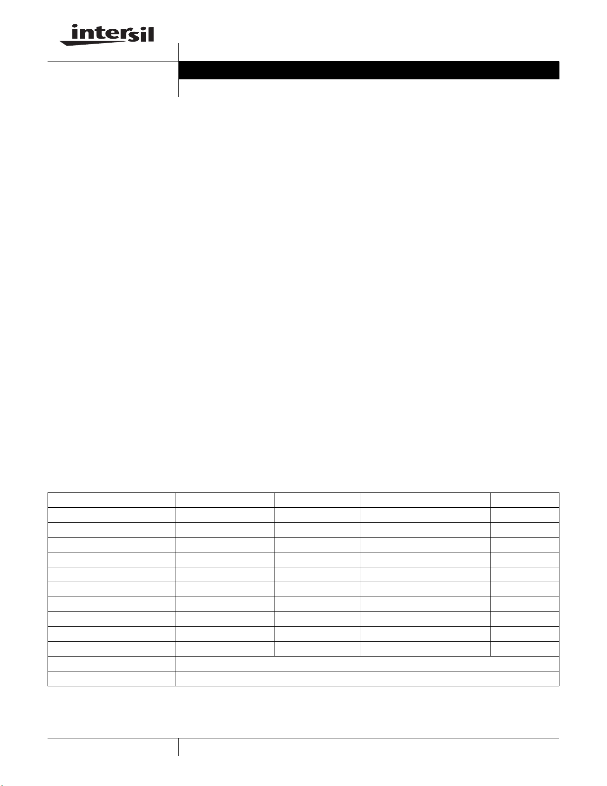
Ordering Information
PART NUMBER PART MARKING TEMP. RANGE (°C) PACKAGE PKG. DWG. #
ISL6549CB ISL6549CB 0 to 70 14 Ld SOIC M14.15
ISL6549CBZ (Note) 6549CBZ 0 to 70 14 Ld SOIC (Pb-free) M14.15
ISL6549CR ISL6549CR 0 to 70 16 Ld 4x4 QFN L16.4x4
ISL6549CRZ (Note) 6549CRZ 0 to 70 16 Ld 4x4 QFN (Pb-free) L16.4x4
ISL6549CA ISL6549CA 0 to 70 16 Ld QSOP M16.15A
ISL6549CAZ (Note) 6549CAZ 0 to 70 16 Ld QSOP (Pb-free) M16.15A
ISL6549CAZA (Note) 6549CAZ 0 to 70 16 Ld QSOP (Pb-free) M16.15A
ISL6549IBZ (Note) 6549IBZ -40 to 85 14 Ld SOIC (Pb-free) M14.15
ISL6549IRZ (Note) 6549IRZ -40 to 85 16 Ld 4x4 QFN (Pb-free) L16.4x4
ISL6549IAZ (Note) 6549IAZ -40 to 85 16 Ld QSOP (Pb-free) M16.15A
ISL6549LOW-EVAL1 Evaluation Board 1-5A
ISL6549HI-EVAL1 Evaluation Board up to 20A
Add “-T” suffix for tape and reel.
NOTE: Intersil Pb-free plus anneal products employ special Pb-free material sets, molding compounds/die attach materials and 100% matte tin plate
termination finish, which are RoHS compliant and compatible with both SnPb and Pb-free soldering operations. Intersil Pb-free products are MSL
classified at Pb-free peak reflow temperatures that meet or exceed the Pb-free requirements of IPC/JEDEC J STD-020.
1
CAUTION: These devices are sensitive to electrostatic discharge; follow proper IC Handling Procedures.
1-888-INTERSIL or 1-888-468-3774
All other trademarks mentioned are the property of their respective owners.
| Intersil (and design) is a trademark of Intersil Americas Inc.
Copyright © Intersil Americas Inc. 2004, 2006. All Rights Reserved
Page 2
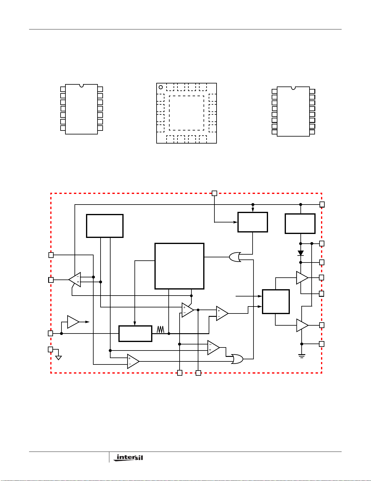
Pinouts
ISL6549 (SOIC)
TOP VIEW
BOOT
1
2
FS_DIS
3
COMP
FB
4
GND
5
6
7
LDO_DR
LDO_FB
Block Diagram
14
13
12
11
10
9
8
UGATE
PHASE
PGND
LGATE
PVCC5
VCC5
VCC12
COMP
FB
LDO_DR
LDO_FB
ISL6549
ISL6549 (QFN)
TOP VIEW
FS_DIS
1
2
(BOTTOM)
3
4
AGND
BOOT
UGATE
PHASE
1516 14 13
12
METAL
GND
PAD
11
10
9
6578
DGND
VCC12
VCC12
VCC5
PGND
LGATE
PVCC5
VCC5
BOOT
FS_DIS
COMP
FB
LDO_DR
LDO_FB
AGND
DGND
ISL6549 (QSOP)
TOP VIEW
1
2
3
4
5
6
7
8
16
15
14
13
12
11
10
9
UGATE
PHASE
PGND
LGATE
PVCC5
VCC5
VCC12
VCC12
LDO_FB
LDO_DR
FS_DIS
GND
EA2
DIS
VOLTAGE
REFERENCE
0.80V
0.60V
OSCILLATOR
UV2
SOFT-START
EA1
FB
RESTART
INHIBIT
SOFT-START
COMP
UV1
COMP
POWER-ON
RESET (POR)
DIS
PWM
VCC12
5V
REGULATOR
PVCC5
BOOT
UGATE
PHASE
GATE
LOGIC
LGATE
PGND
2
FN9168.2
September 22, 2006
Page 3
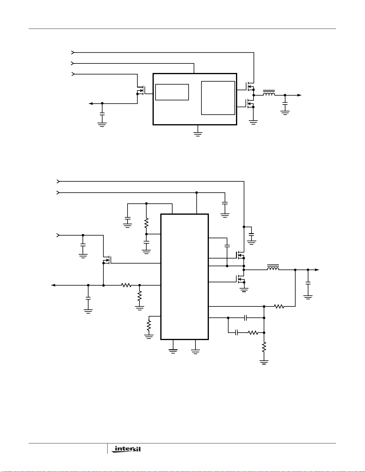
Simplified Power System Diagram
+V
IN1
+12V
+V
IN2
ISL6549
V
OUT2
+
Typical Application Schematic
+V
IN1
+12V
C
BP
+V
IN2
C
+
VIN2
Q3
Q3
LINEAR
CONTROLLER
PWM
CONTROLLER
Q1
Q2
V
OUT1
+
ISL6549
C
BP12
PVCC5
VCC5
C
BP5
LDO_DR
VCC12
BOOT
UGATE
PHASE
C
BOOT
Q1
+
C
VIN1
L
OUT
V
OUT1
V
OUT2
LDO_FB
+
C
OUT2
FS_DIS
GND
LGATE
ISL6549
FB
COMP
PGND
Q2
3
+
C
OUT1
FN9168.2
September 22, 2006
Page 4
ISL6549
Absolute Maximum Ratings Thermal Information
VCC12 . . . . . . . . . . . . . . . . . . . . . . . . . . . . . . . .GND - 0.3V to +14V
PVCC5, VCC5 . . . . . . . . . . . . . . . . . . . . . . . . . . .GND - 0.3V to +7V
VCC5 (if used with external supply). . . . . . . . . . .GND - 0.3V to +6V
BOOT. . . . . . . . . . . . . . . . . . . . . . . . . . . . . . . . . GND - 0.3V to +27V
PHASE. . . . . . . . . . . . . . . . . . . . . . . . V
V
- V
BOOT
UGATE. . . . . . . . . . . . . . . . . . . . . .V
LGATE. . . . . . . . . . . . . . . . . . . . . . . . GND - 0.3V to PVCC5 + 0.3V
. . . . . . . . . . . . . . . . . . . . . . . . . . . . . . . . . . . . .+7V
PHASE
PHASE
BOOT
- 0.3V to V
- 7V to V
BOOT
BOOT
+ 0.3V
+ 0.3V
LDO_DR . . . . . . . . . . . . . . . . . . . . . . GND - 0.3V to VCC12 + 0.3V
FB, LDO_FB, COMP, FS_DIS . . . . . . . GND - 0.3V to VCC5 + 0.3V
ESD Classification
Human Body Model (Per JESD22-A114C) . . . . . . . . . . . . . . Class 2
Machine Model (Per EIA/JESD22-A115-A) . . . . . . . . . . . . . .Class B
Charge Device Model (Per JESD22-C101C). . . . . . . . . . . . Class IV
CAUTION: Stresses above those listed in “Absolute Maximum Ratings” may cause permanent damage to the device. This is a stress only rating and operation of the
device at these or any other conditions above those indicated in the operational sections of this specification is not implied.
NOTES:
is measured with the component mounted on a high effective thermal conductivity test board in free air. See Tech Brief TB379 for details.
1. θ
JA
is measured in free air with the component mounted on a high effective thermal conductivity test board with “direct attach” features. See
2. θ
JA
Tech Brief TB379.
3. For θ
, the “case temp” location is the center of the exposed metal pad on the package underside.
JC
Thermal Resistance θ
(°C/W) θJC (°C/W)
JA
SOIC Package (Note 1) . . . . . . . . . . . . 105 N/A
QFN Package (Notes 2, 3). . . . . . . . . . 52 14
QSOP Package (Note 1) . . . . . . . . . . . 110 N/A
Maximum Junction Temperature (Plastic Package) . . . . . . +150°C
Maximum Storage Temperature Range. . . . . . . . . -65°C to +150°C
Maximum Lead Temperature (Soldering 10s) . . . . . . . . . . . +300°C
(SOIC - Lead Tips Only)
Recommended Operating Conditions
External Supply Voltage on VCC5. . . . . . . . . . . . . . . . . . +5.0V ±5%
Supply Voltage on VCC12. . . . . . . . . . . . . . . . . . . . . . . +12V ±10%
Ambient Temperature Range (C). . . . . . . . . . . . . . . . . . 0°C to 70°C
Ambient Temperature Range (I) . . . . . . . . . . . . . . . . -40°C to +85°
Junction Temperature Range. . . . . . . . . . . . . . . . . . . 0°C to +125°C
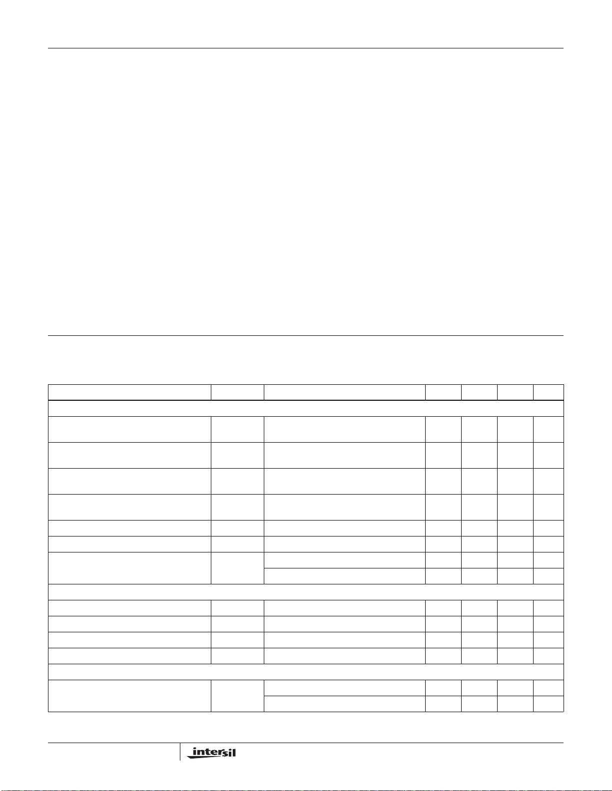
Electrical Specifications Recommended Operating Conditions, unless otherwise noted. VCC12 = 12V
Temperature = 0 to +70°C (typical = +25°C) for Commercial; Temperature = -40 to + 85°C (typical = +25°C) for
Industrial. Refer to Block Diagram, Simplified Power System Diagram, and Typical Application Schematic.
PARAMETER SYMBOL TEST CONDITIONS MIN TYP MAX UNITS
VCC SUPPLY CURRENT
Nominal Supply Current VCC12 (disabled) I
Nominal Supply Current VCC5 (disabled) I
Nominal Supply Current VCC12
CC12 dis
CC5 dis
I
CC12
(includes PVCC5 current)
Nominal Supply Current VCC5 I
Maximum PVCC5 Current Available (Note 5) I
VCC12 to PVCC5 Current Limit (Note 5) I
PVCC5 Voltage V
CC5
PVCC5
PVCC5CL
PVCC5
POWER-ON RESET
Rising VCC5 Threshold VCC12 = 12V 3.7 4.2 4.5 V
Falling VCC5 Threshold VCC12 = 12V 3.3 3.8 4.1 V
Rising VCC12 Threshold VCC5 = 5V 8.8 9.5 10.0 V
Falling VCC12 Threshold VCC5 = 5V 7.0 7.5 8.0 V
OSCILLATOR AND SOFT-START
Switching Frequency F
OSC
UGATE, LGATE and LDO_DR open;
23mA
FS_DIS = GND
UGATE, LGATE and LDO_DR open;
57.5mA
FS_DIS = GND (Note 4)
UGATE, LGATE and LDO_DR open;
F
= 620kHz
OSC
UGATE, LGATE and LDO_DR open;
F
= 620kHz
OSC
12 18 mA
46mA
100 mA
150 mA
ISL6549C; No external load 4.95 5.25 5.8 V
ISL6549I; No external load 4.85 5.25 5.8
ISL6549C; R
ISL6549I; R
= 45.3kΩ 540 620 700 kHz
FS_DIS
= 45.3kΩ 525 620 700 kHz
FS_DIS
4
FN9168.2
September 22, 2006
Page 5
ISL6549
Electrical Specifications Recommended Operating Conditions, unless otherwise noted. VCC12 = 12V
Temperature = 0 to +70°C (typical = +25°C) for Commercial; Temperature = -40 to + 85°C (typical = +25°C) for
Industrial. Refer to Block Diagram, Simplified Power System Diagram, and Typical Application Schematic.
(Continued)
PARAMETER SYMBOL TEST CONDITIONS MIN TYP MAX UNITS
Sawtooth Amplitude (Note 6) DV
Soft-Start Interval T
OSC
SS
F
= 620kHz 6.8 ms
OSC
REFERENCE VOLTAGE
Reference Voltage V
REF
ISL6549C; For Error Amp 1 and 2 0.792 0.8 0.808 V
ISL6549I; For Error Amp 1 and 2 0.788 0.8 0.812 V
PWM CONTROLLER ERROR AMPLIFIER
DC Gain (Note 6) R
Gain-Bandwidth Product (Note 6) GBWP R
Slew Rate (Note 6) SR R
= 10K, CL = 10pF 96 dB
L
= 10K, CL = 10pF 20 MHz
L
= 10K, CL = 10pF 8 V/µs
L
FB Input Current ⎜II ⎜ VFB = 0.8V 0.1 1.0 µA
COMP High Output Voltage V
COMP Low Output Voltage V
COMP High Output, Source Current I
Undervoltage Level (V
FB/VREF
)V
High 4.8 V
OUT
Low 0.6 V
OUT
High -2.8 mA
OUT
UV
70 75 80 %
PWM CONTROLLER GATE DRIVERS
UGATE Maximum Voltage V
LGATE Maximum Voltage V
UGATE and LGATE Minimum Voltage V
UGATE Source Output Impedance R
UGATE Sink Output Impedance R
LGATE Source Output Impedance R
LGATE Sink Output Impedance R
HUGATE
HLGATE
LGATE
DS(ON)
DS(ON)
DS(ON)
DS(ON)
VCC12 = 12V; PHASE = 12V 17 17.5 18
VCC12 = 12V; based on PVCC5 voltage 5.25 6 V
VCC12 = 12V; PHASE = 0V 0 0.5 V
VCC12 = 12V; I
VCC12 = 12V; I
VCC12 = 12V; I
VCC12 = 12V; I
= 100mA 0.8 Ω
GATE
= 100mA 0.7 Ω
GATE
= 100mA 0.8 Ω
GATE
= 100mA 0.4 Ω
GATE
LINEAR REGULATOR (LDO_DR)
DC Gain (Note 6) Gain R
Gain-Bandwidth Product (Note 6) GBWP R
Slew Rate (Note 6) SR R
LDO_FB Input Current ⎜I
LDO_DR High Output Voltage V
LDO_DR Low Output Voltage V
LDO_DR High Output Source Current I
LDO_DR Low Output Sink Current I
Undervoltage Level (V
LDO_FB/VREF
)VUVPercent of Nominal 70 75 80 %
⎜ V
I
High VCC12 = 12V 11.0 11.5 V
OUT
Low 0.0 0.5 V
OUT
High V
OUT
Low 0.5 mA
OUT
= 10K, CL = 10pF 100 dB
L
= 10K, CL = 10pF 2 MHz
L
= 10K, CL = 10pF 6 V/µs
L
= 0.8V 0.1 1.0 µA
LDO_FB
= 2.0V 2.0 mA
OUT
NOTES:
4. Current in VCC5 is actually higher disabled, due to extra current required to pull down against the FS_DIS pin. VCC12 current is lower disabled.
5. Guaranteed by design, not production tested. Exceeding the maximum current from PVCC5 may result in degraded performance and unsafe
operation.
6. Guaranteed by design, not production tested.
1.5 V
5
FN9168.2
September 22, 2006
Page 6

ISL6549
Functional Pin Description
VCC12
This is the power supply pin for the IC; it sources the internal
5V regulator used for the gate drivers. Provide a local
decoupling capacitor to GND. The voltage at this pin is
monitored for Power-On Reset (POR) purposes. The
16 Ld QFN and 16 Ld QSOP have two VCC12 pins; tie them
together on the board.
VCC5
This pin supplies the internal 5V bias for analog and logi c
functions. Provide a local decoupling cap acitor to GN D, and a
resistor to PVCC. The voltage at this pin is monitored for
Power-On Reset (POR) purposes. See “Internal PVCC5
Regulator” on page 7 for more details.
GND, AGND, DGND
These pins are the signal ground for the IC. All voltage levels
are measured with respect to these pins. Connect all to the
ground plane via the shortest available path.
PVCC5
This pin is the internal 5V linear regulator for the BOOT supply
(for the UGATE driver), and the source for the LGATE.
Provide a local decoupling capacitor to PGND. Do not use this
pin as a voltage source for other ci rcuits. See “Internal PVCC5
Regulator” on page 7 for more details.
PGND
This pin is the power ground return for the lower gate driver.
(LGA TE). Connect to the groun d plane on the boa rd via the
shortest available path.
UGATE
This output pin drives the upper MOSFET gate from the
internal 5V regulator . Connect it to the gate of the uppe r
MOSFET via a short, low inductance trace.
BOOT
The BOOT pin, along with the external capacitor (from
PHASE to BOOT), an internal diode, and the internal 5.5V
regulator, creates the boot strap vo lt age for the upper g ate
driver (UGA TE). The maximum voltag e is around 5.5V (above
PHASE).
PHASE
This pin represents the return path for the upper gate drive.
Connect it to the source of the upper MOSFET via a short, low
inductance trace.
FB
FB is the available external inverting input pin of the error
amplifier. Connect the output of the switching regulator to
this pin through a properly sized resistor divider, to set the
output voltage. The voltage at this pin is regulated to the
internal reference voltage. This pin is also monitored for
undervoltage detection.
COMP
COMP is the available external output pin of the error amplifier.
This pin is used to compensate the voltage-mode control
feedback loop of the standard synchronous rectified buck
converter. Connect an appropriate compensation network
between this and the FB pin. See “PWM Controller Feedback
Compensation” on page 10 for more information.
FS_DIS
This input pin has two functions. A resistor to GND sets the
internal oscillator frequency for the switching regulator. In
addition, if the pin is pulled down towards GND with a low
impedance (<1kΩ, such as an external FET), it will disable
both regulator outputs until released (at which time a new softstart cycle will begin).
LDO_DR
This output pin provides the gate voltage for the linear
regulator pass transistor . Connect this pin to the gate terminal
of an external N-channel MOSFET transistor. This pin (along
with the LDO_FB pin) also provides a means of compensating
the error amplifier, sh ould the appli cation re quire it.
LDO_FB
This input pin is the FB inverting input on the linear regulator
error amplifier. Conn ect the output of the line ar regulator to
this pin through a properly sized resistor divider , to set the
output voltage. The voltage at this pin is regulated to the
internal reference voltage. This pin is also monitored for
undervoltage detection.
Bottom Pad (QFN Package Only)
The QFN package’s metal bottom pad is resistively tied to the
internal IC GND. For best thermal and electrical performance,
connect this pad to the GND pins, and to the ground plane of
the PCB through 4 vias equidistantly situated inside the solder
landing pad.
LGATE
This output pin drives the lower MOSFET gate from the
internal 5V regulator. Connect it to the gate of the lower
MOSFET via a short, low inductance trace.
6
FN9168.2
September 22, 2006
Page 7
ISL6549
Description
Operation Overview
The ISL6549 monitors and precisely controls two output
voltage levels. Refer to the “Block Diagram” on page2,
“Simplified Power System Diagram” on page 3, and “Typical
Application Schematic” on page 3. The controller is intended
for use in applications where only a 12V bias input is
available. The IC integrates both a standard buck PWM
controller and a linear controller . The PWM control ler
regulates the output voltage (V
by a resistor divider. The linear controller is designed to
regulate the lower current local memory voltage (V
through an external N-Channel MOS pass transistor.
Internal PVCC5 Regulator
The preferred and recommended configuration is as follows:
+12V to VCC12 pin, a resistor (~10Ω) between PVCC5 and
VCC5 pins, and decoupling caps on all three pins to ground.
This creates the PVCC5 voltage for the gate drivers, and
externally filters it for bias on the VCC5 pin. It also guarantees
that all 3 voltages track each other during power-up and
power-down.
The PVCC5 pin cannot be used as an i nput and it should not
be used as an output for other circuits; its current capability is
reserved for the gate drivers and VCC5 bias. Similarly, the
VCC5 pin should not be used as an output. Although not
preferred, the VCC5 pin can be used with an external 5V
supply (±5%). However, proper precautions must be foll owed,
which mainly have to do with proper sequencing, to prevent
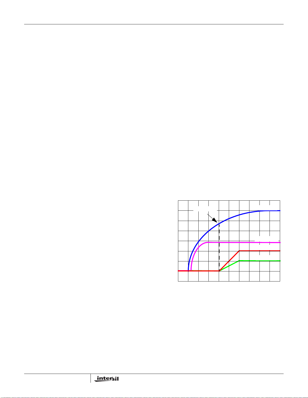
latch-up or related problems. Note in the power-up diagram
(Figure 1), the 5V lags the 12V by a few msecs and a volt or
so; that is expected. Both the VCC12 and VCC5 pins must
exceed their rising POR trip points before the soft-start is
enabled; the trip order is not important as long as both have
some voltage. The 12V can be present with no 5V at all, but
the 5V should not precede the 12V. Similarly, on power down,
the 5V should discharge with or before the 12V.
Under normal operation, the internal regulator can supply up
to 100mA (which includes the VCC5 bias current, with the
resistor between the pins). The amount of current is
determined primarily by the switching parameters: the
oscillator frequency and the loading of the FET gates.
Overloading of the internal regulator is not recommended;
even if there is enough current, the gate driver waveforms
may be degraded. See “Switcher FET Considerations” on
page 13 for more details.
The PVCC5 pin has a current limit that provides some
protection against a shorted gate driver dragging down the
12V rail. The temperature of the IC will increase as the current
and corresponding on-chip power dissipation increases.
There is no thermal shutdown, so even if the current limit is
effective, the IC can be subject to very high temperatures. If
the current limit is exceeded, the regulator voltage will likely
) to a level programmed
OUT1
OUT2
)
collapse, shutting down everything until the load current is
reduced or removed.
Initialization
The ISL6549 automatically initializes upon application of input
power (at the VCC12) pin. The ISL6549 creates its own
PVCC5 and VCC5 supplies for internal use. The POR
function continually monitors the input bias supply voltage at
the VCC12 and VCC5 pins. The POR function initiates softstart operation after both these supply voltages exceed their
POR rising threshold voltages.
Soft-Start
The POR function initiates the digital soft-st art sequence. Both
the linear regulator error amplifier and PWM error amplifier
reference inputs are forced to track a voltage level
proportional to the soft-start voltage. As the sof t-st art volt ag e
slews up, the PWM comparator regulates the output relative
to the tracked soft-start voltage, slowly charging the output
capacitor(s). Simultaneously, the linear output follows the
smooth ramp of the soft-start function into normal regulation.
Figure 1 shows the soft-start sequence. Both the VC C12 and
VCC5 pins must be above their respective rising POR trip
points. In most cases, as shown here, the last one excee ding
its threshold is the VCC12 around 9.5V. The ramp time is
based on the internal oscillator period multiplied by 4096. So
for a 600kHz (1.67µs) example, the soft-start ramp time would
be 6.8ms.
VCC12 > 9.5V
GND>
GND>
GND>
GND>
FIGURE 1. 12V POWER-UP INTO SOFT-START
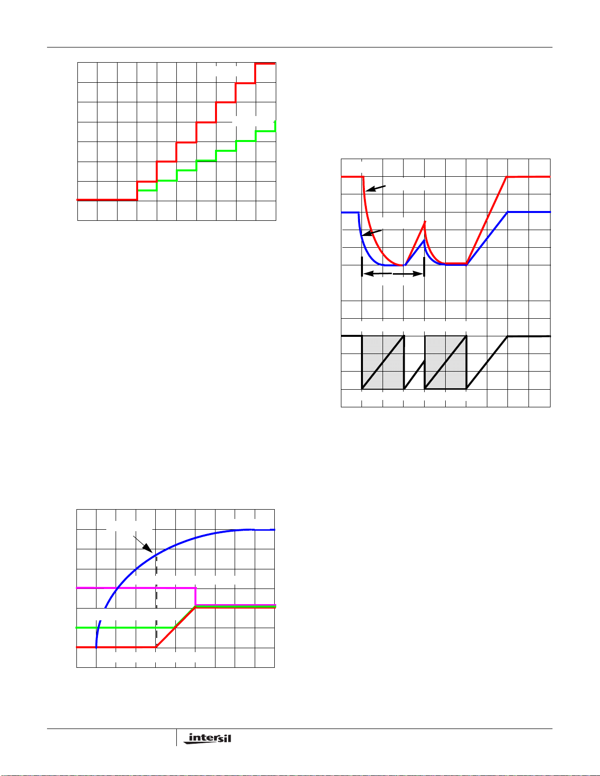
Figure 2 shows more detail of the output ramps, by increasing
the time and voltage resolution. The clock for the DAC
producing the steps is approximately 9.4kHz (600kHz/64), so
each step is just over 100µs long. The step voltage is 1/64 of
the final value for each output; around 31mV for V
15.6mV for V
in this example. By providing many small
OUT2
steps of voltage (and current) that effectively charg e the
output capacitor, the potentially large peak current resulting
from a sudden, uncontrolled voltage rise are eliminated, by
spreading it out over the whole ramp time.
VCC12 (2V/DIV)
VCC5 (2V/DIV)
V
(1V/DIV)
OUT1
V
(1V/DIV)
OUT2
and
OUT1
7
FN9168.2
September 22, 2006
Page 8
ISL6549
.
V
OUT1
V
OUT2
GND>
GND>
FIGURE 2. EXPANDED VIEW: VOLTAGE RAMP AND TIME
A few clock cycles are used for initialization to insure that softstart begins near zero volts. The ramp s are the same, whether
triggered by releasing FS_DIS or by exceeding the POR trip
levels.
Both outputs use the same soft-start ramp, and the ramp time
is determined by the switching frequency . Thu s, there is no
simple way to disable or sequence them independently, or to
change the ramp rate independently of the clock.
Undervoltage Protection
The FB and LDO_FB pins are each monitored during
converter operation by their own Undervoltage (UV)
comparator. If ei ther FB vo lt age drops below 75% of the
reference voltage (75% of 0.8V = 0.6V), a fault signal is
internally generated, and the fault logic shuts down BOTH
regulators. The UV comparators are enabled when the
soft-start ramp is about one-quarter (25%) done.
(0.5V/DIV)
V
(2.5V)
OUT2
V
(1.5V)
OUT1
GND>
GND>
DELAY INTERVAL
INTERNAL SOFT-START FUNCTION
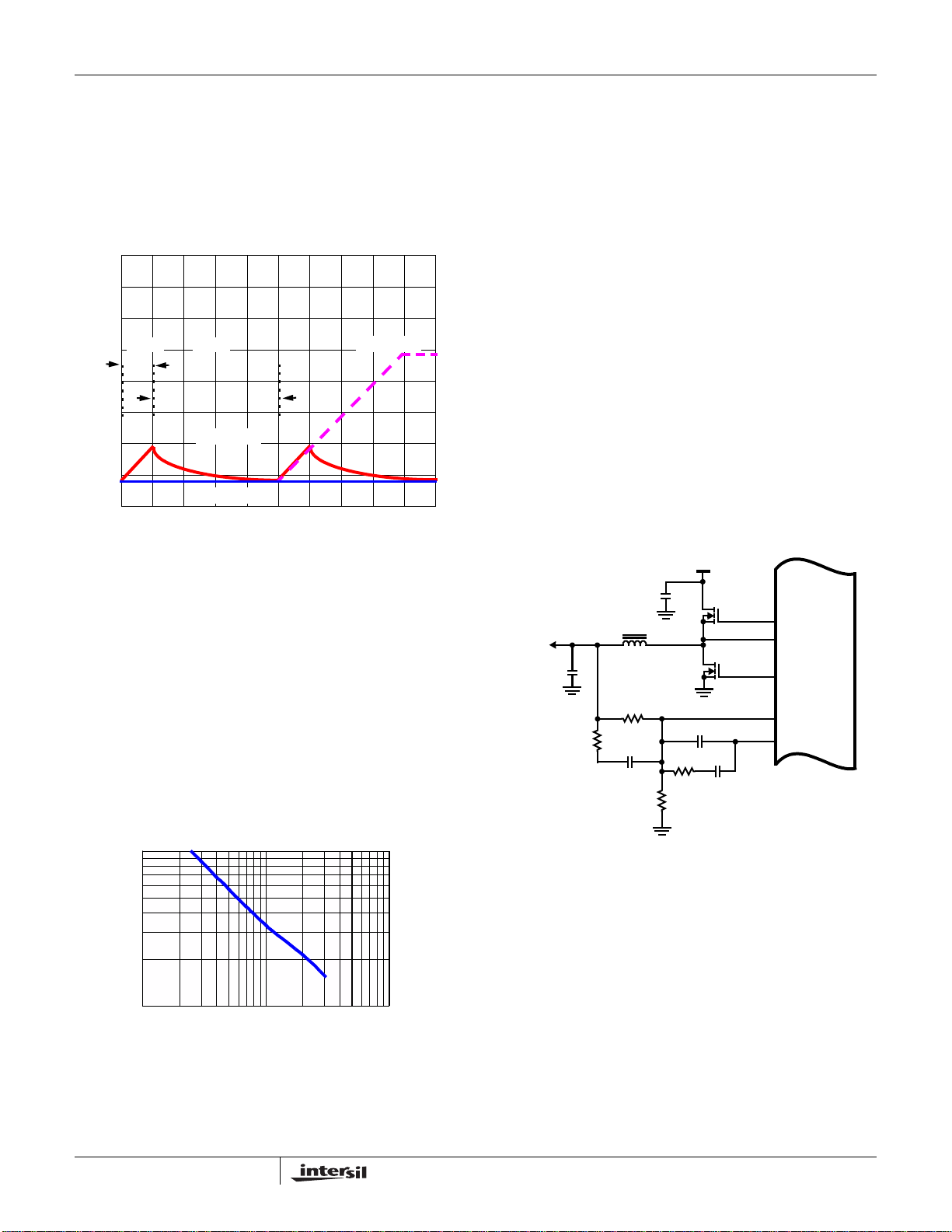
If the switcher output is already pre-charged to a voltage when
the regulator starts up, the ISL6549 will detect this condition
(see Figure 3). The red trace shows the normal ramp, when
the output starts at GND. The green trace shows the case
when the output is pre-charged to a voltage less than the final
output. The upper or lower FET does not turn on until the sof tstart ramp voltage exceeds the output; then the output starts
ramping seamlessly from there. If the output voltage is precharged above the normal output level, as shown in the
magenta trace, neither FET will turn on until the end of the
soft-start ramp; then the output will be quickly pulled down to
the final value.
VCC12 (2V/DIV)
GND>
GND>
GND>
GND>
VCC12 > 9.5V
V
OVER-CHARGED (1V/DIV)
OUT2
V
PRE-CHARGED (1V/DIV)
OUT2
V
NO CHARGE (1V/DIV)
OUT2
FIGURE 3. PRE-CHARGED OUTPUT
GND>
FIGURE 4. UNDERVOLTAGE PROTECTION RESPONSE
SOFT-START
DELAY
T0 T4
(T1 TO T2 NOT TO SCALE)
T1 T2
SOFT-START
DELAY
TIME
T3
Figure 4 illustrates the protection feature responding to a UV
event on V
. At time T0, V
OUT1
has dropped below 75%
OUT1
of the nominal output voltage. Both outputs are quickly shut
down and the UGA TE and LGA TE stop switching immediately ,
but the fall time of each output is determined by the load
and/or short condition on each plus the output capacitance
that needs to be discharged. The soft-start function begins
producing an internal soft-start ramp. The de lay interval, T0 to
T1, seen by the output is equivalent to one soft-start cycle.
Then a normal soft-start ramp of the output st art s, at ti me T1.
At the one-quarter point of the soft-start ramp (not drawn
exactly to scale), the good output will have ramped onequarter way up, while the shorted output will presumably be
lower than a quarter (depending on the magnitude of the
short). Once the UV comparators are enabled (at the
one-quarter point) both outputs will again shut down (if the
fault is still present on one of them). Time T2 st art s a new
internal soft-start cycle, and at T3, starts a new ramp, similar
to T1. This time, if we assume the short has gone away , the
outputs will ramp up to T4 as they should. If the short has not
gone away , then the T0, T1, T2 hi ccup mode cycle will keep
repeating indefinitely; this cycle time is the equivalent of 1.25
8
FN9168.2
September 22, 2006
Page 9
ISL6549
soft-start cycles (1 internal soft-start ramp cycle, plus
one-quarter on the next).
If either V
UV shutdown and restart cycle; similarly, if either V
voltage is not present at startup, that will cause a
INx
INx
is
removed after start-up, a shutdown and re st art cycl e wil l st art
when its output drifts down to the UV trip point. But in both
cases, once the V
is restored, the V
INx
will recover on
OUTs
the next soft-start ramp.
V
1.6ms
GND>
GND>
FIGURE 5. UNDERVOLTAGE PROTECTION (SIMULATED BY
6.4ms
V
(0.5V/DIV)
OUT2
V
(0.5V/DIV)
OUT1
HAVING NO VIN1 ON POWER-UP)
Figure 5 shows an example of the start-up, with V
powered. V
ramps up one-quarter of the way, at which
OUT2
time the UV comparators are enabled. Since V
present, V
will not be following the soft-start ramp up,
OUT1
OUT2
IN1
(0.5V/DIV)
not
IN1
is not
and it will fail the test for UV, shutting down both outputs. It
starts an internal delay time-out (equal to one sof t-st art
interval), and then starts a new ramp. For this example, it
shows about a 1.6ms ramp up, and 6.4ms off, before the next
ramp starts. Thus, the total period of 8ms is based on 1.25
soft-start cycles (one-quarter of the first ramp, an d then one
full time-out, at a clock period of around 1.6µs) The dotted
magenta line shows the case where V
is allowed to
OUT2
ramp all of the way up to 2V.
Switching Frequency
1M
dependence between the resistor chosen and the resulting
switching frequency.
Output Voltage Selection
The output voltage of the PWM converter can be programmed
to any level between V
However, even though the ISL654 9 can run at near 100%
duty cycle at zero load, additional voltage margin is required
above V
to allow for loading. An external resistor divider is
IN1
used to scale the output voltage relative to the referen ce
voltage and feed it back to the inverting input of the error
amplifier (see Figure 7). A typical value for R1 may be 1.00kΩ
(±1% for accuracy), and then R4 (also ±1%) is chosen
according to Equation 1:
R4
R1 0.8V×
--------------------------------------- -=
V
OUT1
0.8V–
R1 is also part of the compensation circuit (see “PWM
Controller Feedback Compensation” on page 10 for more
details), so once chosen for that, it should not be changed to
adjust V
; only chan g e R4 . If the output voltage desired
OUT1
is 0.8V, simply route V
but do not populate R4. V
reference are not available.
V
OUT1
+
C
OUT1
R3
FIGURE 7. OUTPUT VOLTAGE SELECTION OF THE
SWITCHER (V
and the internal reference, 0.8V.
IN1
back to the FB pin through R1,
L
C3
C
OUT
R1
OUT1
IN1
R4
voltages less than the 0.8V
OUT1
V
IN1
+
Q1
Q2
C2
C1
R2
OUT1
)
V
OUT1
0.8 1
(EQ. 1)
ISL6549
UGATE
PHASE
LGATE
FB
COMP
R1
⎛⎞
------- -+
×=
⎝⎠
R4
FREQUENCY (kHz)
100k
10k 100k 1M
R (kΩ)
FIGURE 6. FREQUENCY vs FS RESISTOR
The switching frequency of the ISL6549 is determined by the
value of the FS resistor. The graph in Figure 6 shows the
9
The linear regulator output voltage is also set by means of
an external resistor divider as shown in Figure 8. Select a
value for R5 (typical 1.00kΩ ±1% for accuracy ), and use
Equation 2 to calculate R6 (also ±1%), where V
desired linear regulator output voltage and V
REF
OUT2
is the
is the
internal reference voltage, 0.8V. For an output voltage of
0.8V, simply populate R5 wi th a value less than 5kΩ and do
not populate R6. V
voltages less than the 0.8V
OUT2
reference are not available.
R6
-------------------------------------- -=
V
R5 0.8V×
OUT
0.8V–
2
(EQ. 2)
FN9168.2
September 22, 2006
Page 10
ISL6549
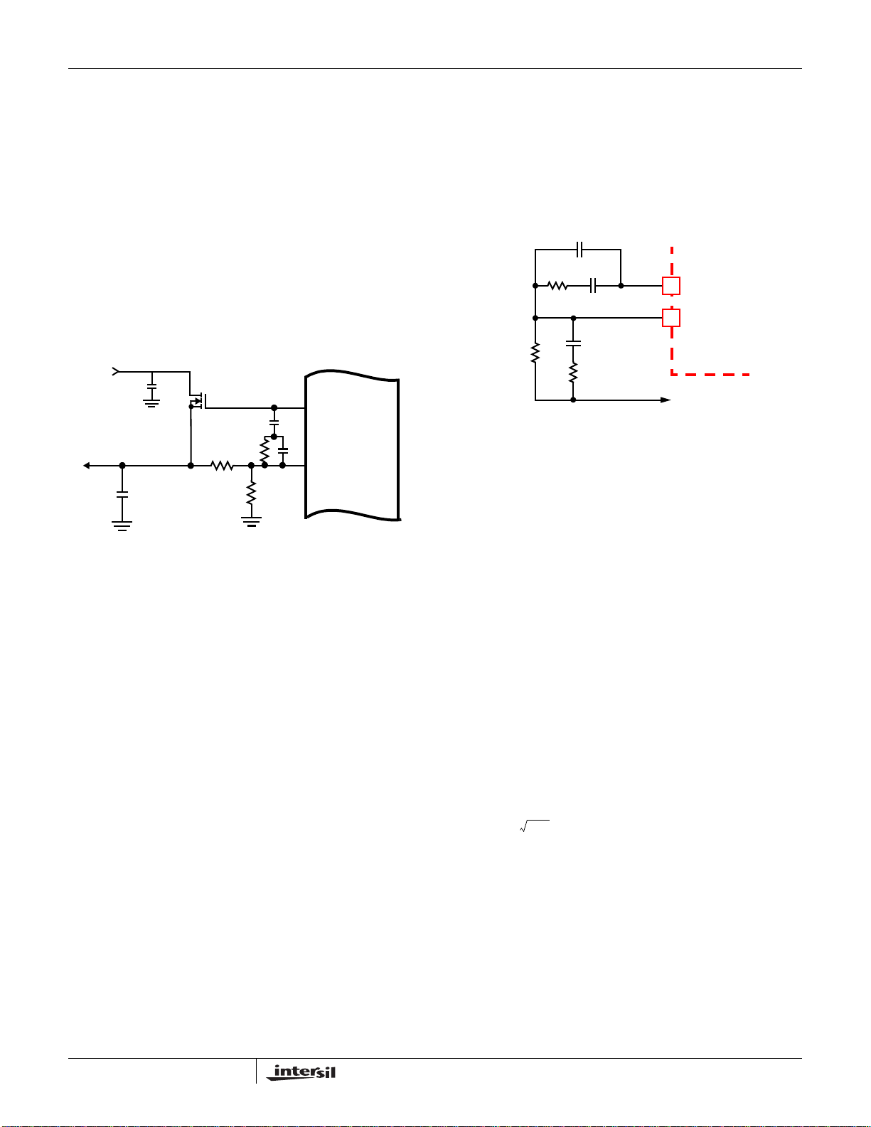
For most situations, no external compensation is required for
the linear output. See “Linear Controller Feedback
Compens a ti on” on page 12.
For both outputs, the selection of 1% resistors may not be
able to get the exact ratio desired for any given ou tput voltage.
If the output must be defined better, then on e option is to
place a much bigger resistor in parallel with R4 or R6, to lower
its value. For example, a 100kΩ in parallel with a 1.00k Ω
yields 990Ω, 1% belo w 1.00kΩ, which gives finer resolution
than the next lower size (976Ω 1%). The big resistor may not
have to be 1% tolerance either .
If the linear output is not required, connect the LDO_DR pin
directly to LDO_FB pin with no other components. This will
terminate the signals and keep the linear from tripping its
undervoltage, which would force both output s into retry.
V
IN2
V
OUT2
C
OUT2
FIGURE 8. OUTPUT VOLTAGE SELECTION OF THE LINEAR
+
C
IN2
+
V
OUT2
(V
OUT2
Q3
0.8 1
)
R5
R6
R5
⎛⎞
------- -+
×=
⎝⎠
R6
LDO_DR
LDO_FB
ISL6549
Converter Shutdown
Pulling and holding the FS_DIS pin near GND will shut down
both regulators; almost any NFET or other pull-down device
(<1kΩ impedance) should work. Upon release of the FS_DIS
pin, the regulators enter into a soft-start cycle which brings
both outputs back into regulation. The FS_DIS pin re quires a
quiet GND to minimize jitter. To accomplish this, the FS
resistor and any pull-down device should be placed as close
as possible to the pin, and the GND should be kept away from
the noisy FET GND.
Boot Capacitor, Boot Refresh
A capacitor from the PHASE pin to the BOOT pin is required
for the bootstrap circuit for the Upper Gate. The V
(and thus the PHASE node) is allowed to go as high as a
nominal 12V (±10%) supply. A diode is included on the IC
(anode to PVCC5 pin, cathode to BOOT pin), such that the
PVCC5 (nominally around 5.25V) will be the boots trap supply.
In the event that the UGATE is on for an extended period of
time, the charge on the boot capacitor can start to sag, raising
the R
of the upper FET. The ISL6549 has a circuit that
DS(ON)
detects a long UGATE on-time (32 oscillator clock periods),
voltage
IN1
and forces the LGA TE to go hi gh for one osci llator cycle,
which allows the bootstrap capacitor time to recha rge.
PWM Controller Feedback Compensation
This section highlights the design consideration for a
voltage-mode controller requiring external compensation. To
address a broad range of applications, a type-3 feedback
network is recommended (see Figure 9).
C2
C1
R2
R1
FIGURE 9. COMPENSATION CONFIGURA TION FOR ISL6549
CIRCUIT
C3
R3
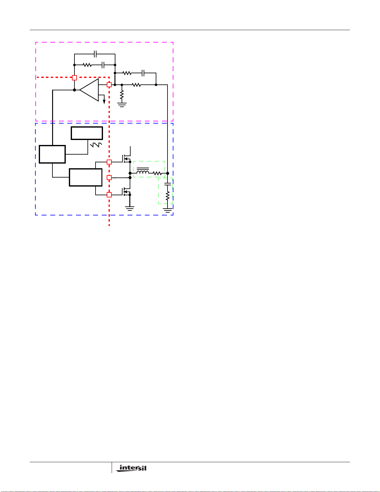
Figure 10 highlights the voltage-mode control loop for a
synchronous-rectified buck converter, applicable to the
ISL6549 circuit. The output voltage (V
reference voltage, VREF . The error amplifier output (COMP pin
voltage) is compared with the oscillator (OSC) modified
saw-tooth wave to provide a pulse-width modulated wave with
an amplitude of V
at the PHASE node. The PWM wave is
IN
smoothed by the output filter (L and C). The output filter
capacitor bank’s equivalent series resistance is represented by
the series resistor E.
The modulator transfer function is the small-signal transfer
function of V
gain, given by d
OUT/VCOMP
MAXVIN/VOSC
filter, with a double pole break frequen cy at F
F
. For the purpose of this analysis, L and D represent the
CE
channel inductance and its DCR, while C and E represents
the total output capacitance and its equivalen t series
resistance.
---------------------------=
2π LC⋅⋅
1
F
LC
The compensation network consists of the error amplifier
(internal to the ISL6549) and the external R1-R3, C1-C3
components. The goal of the compensation network is to
provide a closed loop transfer function with high 0dB crossing
frequency (F
; typically 0.1 to 0.3 of FSW) and adequate phase
0
margin (better than 45 degrees). Phase margin is the difference
between the closed loop phase at F
equations that follow relate the compensation network’s poles,
zeros and gain to the components (R1, R2, R3, C1, C2, and
C3) in Figure 10.
COMP
FB
ISL6549
V
(V
OUT
)
DIFF
) is regulated to the
OUT
. This function is dominated by a DC
, and shaped by the output
and a zero at
LC
F
CE
1
------------------------=
2π CE⋅⋅
and 180°. The
0dB
(EQ. 3)
10
FN9168.2
September 22, 2006
Page 11
ISL6549
C2
C3
R2
COMP
E/A
OSCILLATOR
V
PWM
CIRCUIT
FIGURE 10. VOLT AGE-MODE BUCK CONVERTER
OSC
HALF-BRIDGE
DRIVE
COMPENSATION DESIGN
C1
-
+
VREF
ISL6549
R3
Ro
R1
V
IN
L
FB
UGATE
PHASE
LGATE
EXTERNAL CIRCUIT
V
OUT
D
C
E
Use the following guidelines for locating the poles and zeros of
the compensation network:
1. Select a value for R1 (1kΩ to 5kΩ, typically). Calculate
value for R2 for desired converter bandwidth (F0). If
setting the output voltage via an offset resistor connected
to the FB pin, Ro in Figure 10, the design procedure can
be followed as presented.
V
R1 F
⋅⋅
R2
⋅⋅
d
MAXVINFLC
OSC
---------------------------------------------=
2. Calculate C1 such that F
0
is placed at a fraction of the FLC,
Z1
(EQ. 4)
at 0.1 to 0.75 of FLC (to adjust, change the 0.5 factor to
desired number). The higher the quality factor of the output
filter and/or the higher the ratio F
frequency (to maximize phase boost at F
1
------------------------------------------------=
C1
3. Calculate C2 such that F
C2
⋅⋅⋅
2π R2 0.5 F
---------------------------------------------------------=
2π R2 C1 F
C1
LC
is placed at FCE.
P1
1–⋅⋅⋅
CE
, the lower the FZ1
CE/FLC
LC
).
(EQ. 5)
(EQ. 6)
4. Calculate R3 such that F
is placed at FLC. Calculate C3
Z2
such that FP2 is placed below FSW (typically, 0. 5 to 1.0
times FSW). FSW represents the switching frequency.
Change the numerical factor to reflect desired placement
of this pole. Placement of F
lower in frequency helps
P2
reduce the gain of the compensation network at high
frequency, in turn reducing the HF ripple component at
the COMP pin and minimizing resultant duty cycle jitter.
R3
R1
----------------------=
F
SW
------------ 1–
F
LC
C3
-------------------------------------------------=
2π R3 0.7 F
1
⋅⋅⋅
SW
(EQ. 7)
It is recommended a mathematical model is used to plot the
loop response. Check the loop gain against the error
amplifier’s open-loop gain. Verify phase margin results and
adjust as necessary. Equation 8 describes the frequency
response of the modulator (G
(G
) and closed-loop response (GCL):
FB
d
⋅
G
G
G
MOD
FB
CL
MAXVIN
----------------------------- -
f()
V
OSC
1sf() R2 C1⋅⋅+
------------------------------------------------------
f()
sf() R1 C1 C2+()⋅⋅
---------------------------------------------------------------------------------------------------------------------------- -
⋅
1sf() R3 C3⋅⋅+()1sf() R2
f() G
MOD
----------------------------------------------------------------------------------------
⋅=
1sf() ED+()C⋅⋅s
1sf() R1 R3+()C3⋅⋅+
f() GFBf()⋅=
), feedback compensation
MOD
1sf() EC⋅⋅+
⋅=
⎛⎞
⋅
⎝⎠
⋅⋅+
where s f(), 2π fj⋅⋅=
2
f() LC⋅⋅++
C1 C2⋅
⎛⎞
----------------------
⎝⎠
C1 C2+
(EQ. 8)
COMPENSATION BREAK FREQUENCY EQUATIONS
1
--------------------------------=
F
Z1
2π R2 C1⋅⋅
---------------------------------------------------=
F
Z2
2π R1 R3+()C3⋅⋅
1
F
P1
F
P2
1
-----------------------------------------------=
2π R2
--------------------------------=
2π R3 C3⋅⋅
C1 C2⋅
----------------------
⋅⋅
C1 C2+
1
(EQ. 9)
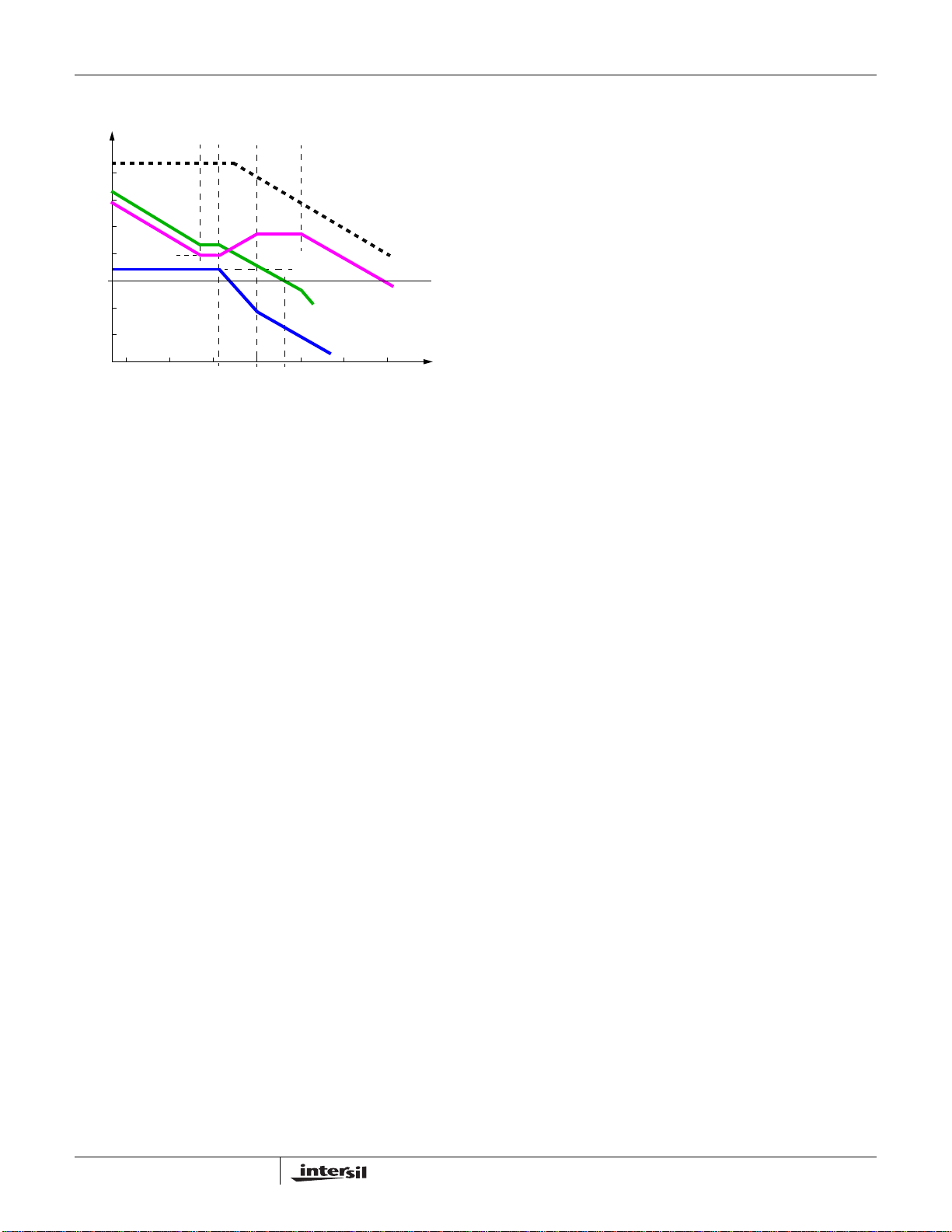
Figure 11 shows an asymptotic plot of the DC-DC converter’s
gain vs. frequency. The actual Modulator Gain has a high gain
peak dependent on the quality factor (Q) of the output filter,
which is not shown. Using the above guidelines should yield a
compensation gain similar to the curve plotted. The open loop
error amplifier gain bounds the compensation gain. Check the
compensation gain at F
amplifier. The closed loop gain, G
log-log graph of Figure 11 by adding the modulator gain, G
(in dB), to the feedback compensation gain, G
against the capabilities of the error
P2
, is constructed on the
CL
(in dB). This is
FB
MOD
equivalent to multiplying the modulator transfer function and the
compensation transfer function and then plotting the resulting
gain.
11
FN9168.2
September 22, 2006
Page 12
F
Z1
GAIN
R2
⎛⎞
------- -
log
20
⎝⎠
R1
0
LOG
LOG
FIGURE 11. ASYMPTOTIC BODE PLOT OF CONVERTER GAIN
F
F
Z2
F
LC
F
P1
F
F
CE
0
MODULATOR GAIN
P2
COMPENSATION GAIN
CLOSED LOOP GAIN
OPEN LOOP E/A GAIN
V
d
⋅
MAX
20
---------------------------------log
V
OSC
G
CL
G
MOD
FREQUENCY
IN
G
FB
A stable control loop has a gain crossing with close to a
-20dB/decade slope and a phase margin greater than 45°.
Include worst case component variations when determining
phase margin. The mathematical model presented makes a
number of approximations and is generally not accurate at
frequencies approaching or exceeding half the switching
frequency . When desi gning compe nsa tion netw orks, select
target crossover frequencies in the range of 10% to 30% of
the switching frequency, F
SW
.
ISL6549
One of the parameters limiting the conve rter’s respo nse to a
load transient is the time required to change the inductor
current. Given a sufficiently fast control loop design, the
ISL6549 will provide either 0% or 100% duty cycle in
response to a load transient. The response time is the time
required to slew the inductor current from an initial current
value to the transient current level. During this interval, the
difference between the inductor current and the transi ent
current level must be supplied by the output capacito r.
Minimizing the response time can minimize the output
capacitance required.
The response time to a transient is different for the application
of load and the removal of load. Equation 11 gives the
approximate response time interval for application and
removal of a transient load:
LOI
LOI
×
RISE
where: I
TRAN
------------------------------- -=
V
–
INVOUT
is the transient load current step, t
TRAN
t
FALL
response time to the application of load, and t
×
TRAN
-------------------------------=t
V
OUT
FALL
RISE
is the
(EQ. 11)
is the
response time to the removal of load. With a +5V input
source, the worst case response time can be either at the
application or removal of load and dependent upon the output
voltage setting. Be sure to check both of these equations at
the minimum and maximum output levels for the worst case
response time.
Linear Controller Feedback Compensation
For most situations, no external compensation is required for
the linear output. As long as the output capacitor (C
OUT2
) is
large (>100µF) and so is its ESR (>20mW), then it should be
stable for loads as low as 10mA up to at least 4A. If smaller
values of capacitance and/or ESR are desired, then special
considerations may be required to add external
compensation (as shown in Figure 8).
Component Selection Guidelines
Output Inductor Selection
The output inductor is selected to meet the output voltage
ripple requirements and minimize the converter’s response
time to the load transient. The inductor value determines the
converter’s ripple current and the ripple voltage is a function of
the ripple current. The ripple voltage and current are
approximated by Equation 10.
- V
V
IN
--------------------------------
∆I =
FSW x L
Increasing the value of inductance reduces the ripple current
and voltage. However , the large inductance values red uce the
converter’s response time to a load transient (and usually
increases the DCR of the inductor, which decreases the
efficiency). Increasing the switching frequency (F
given inductor also reduces the ripple current and voltage.
OUT
V
--------------- -
•
OUT
V
IN
∆V
OUT
= ∆I x ESR
SW
(EQ. 10)
) for a
Output Capacitors Selection
An output capacitor is required to filter the output and supply
the load transient current. The filtering requirements are a
function of the switching frequency and the ripple current. The
load transient requirements are a function of the slew rate
(di/dt) and the magnitude of the transient load current. These
requirements are generally met with a mix of capacitors and
careful layout.
Modern microprocessors produce transient load rates above
1A/ns. High frequency capacitors initially supply the transient
and slow the current load rate seen by the bulk capacitors.
The bulk filter capacitor values are generally determined by
the ESR (effective series resistance) and voltag e rating
requirements rather than actual capacitance requirements.
High frequency decoupling capacitors should be placed as
close to the power pins of the load as physically possible. Be
careful not to add inductance in the circuit board wiring that
could cancel the usefulness of these low inductance
components. Consult with the manufacturer of the load on
specific decoupling requirements. And keep in mind that not all
applications have the same requirements; some may need
many ceramic capacitors in parallel; others may need only one.
Use only specialized low-ESR capacitors intended for
switching-regulator applications for the bulk capacitors.
The bulk capacitor’s ESR will determine the output ripple
voltage and the initial voltage drop after a high slew-rate
12
FN9168.2
September 22, 2006
Page 13

ISL6549
transient. An aluminum electrolytic capacitor's ESR value is
related to the case size with lower ESR available in larger
case sizes. However, the equivalent series inductance
(ESL) of these capacitors increases with case size and can
reduce the usefulness of the capacitor to high slew-rate
transient loading. Unfortunately, ESL is not always a
specified parameter. Work with your capacitor supplier and
measure the capacitor’s impedance with frequency to
select a suitable component. In most cases, multiple
electrolytic capacitors of small case size perform better
than a single large case capacitor.
Input Capacitor Selection
Use a mix of input bypass capacitors to control the volt age
overshoot across the MOSFETs. Use small ceramic
capacitors for high frequency decoupling and bulk cap acito rs
to supply the current needed each time Q1 turns on. Place the
small ceramic capacitors physically close to the MOSFETs
and between the drain of upper FET Q1 and the source of
lower FET Q2.
The important parameters for the bulk input capaci tor are the
voltage rating and the RMS current rating. For reliable
operation, select the bulk capacitor with voltage and current
ratings above the maximum input voltage and largest RMS
current required by the circuit. The capacitor voltage rating
should be at least 1.25 times greater than the maximum input
voltage and a voltage rating of 1.5 times is a conservative
guideline. The RMS current rating requirement for the input
capacitor of a buck regulator is approximately half the DC load
current. Several electrolytic capacitors may be needed.
Bootstrap Capacitor Selection
The boot diode is internal to the ISL6549, and uses PVCC5 to
charge the external boot capacitor . The size of the b oot strap
capacitor can be chosen by using the equations in Equation
12.
Q
GATE
C
BOOT
--------------------
≥ Q
∆V
and
GATE
where
N is the number of upper FETs
QG is the total gate charge per upper FET
V
is the input voltage
IN
V
is the gate-source voltage (~5V for ISL6549)
GS
∆V is the change in boot voltage before and immediately
after the transfer of charge; typically 0.7V to 1.0V
C
BOOT
Q
--------------------
GATE
∆V
NQ
••
GVIN
----------------------------------
∆V•
V
GS
The last equation plugs in some typical values: N = 1;
Q
is 33nC, VIN is 12V, VGS is 11V, ∆V
G
example, C
≥ 0.113µF . This value is o fte n rou nded to
BOOT
NQGVIN••
----------------------------------=
13312••
--------------------------- -
50.7•
max
V
GS
0.113µ F===≥
= 1V. In this
(EQ. 12)
0.1µF or 0.22µF as a starting value. The boot strap capa citors
for the ISL6549 can usually be rated for 6.3V.
Switcher FET Considerations
The IC was designed for nominal 12V supply for V
upper FET Q1). However, it wil l work with mo st any volt age
(from other supplies or other regulator outputs) down to
around 1V, as long as the input is above the output by a
sufficient margin (based on practical duty cycle limit ations and
upper FET R
constraints). For example, although the
DS(ON)
IC can function at near 100% duty cycle, the voltage drop due
to the R
DS(ON)
of the upper FET at full load current will limit
the practical duty cycle to something less than 100%. So the
V
range is roughly 1.0V up to 12V, with the V
IN1
slightly below it. Therefore, the FETs need to be rated for
drain-source breakdown above the V
voltage; 20V and
IN1
30V ratings are common.
The ISL6549 gate drivers (UGA TE and LGATE) were
designed to drive up to 2 upper and 2 lower 8 Ld SOIC FETs;
when the FETs are properly sized, the output currents can
range from under 1A to over 20A. Driving more or bigger FETs
is not recommended; even if there is enough current (from the
internal PVCC5 regulator), the gate driver waveforms may be
degraded. DPAK FET packages can be used, but D
FETs are not recommended, due to the higher inductance of
the package leads. For example, the inductance in the source
of the lower FET can create large negative spikes on the
PHASE node when the UGA TE tu rn s off.
Both the UGA TE and LGATE voltages are derived from the
internal PVCC5 internal regulator , typi cally 5 .25V. UGATE is
only about 5.0V above PHASE, due to the d rop in the internal
BOOT diode charging the BOOT capacitor; LGATE sees the
full 5.25V . So both are consid ered “5V” drivers; this affect s the
FET selection in two ways. First, the FET gate-source voltage
rating can be as low as 12V (this rating is usually consistent
with the 20V or 30V breakdown chosen above). Second, the
FETs must have a low threshold voltage (around 1V), in order
to have its R
rating at VGS = 4.5V in the 10mΩ-20mΩ
DS(ON)
range. While some FETs are also rated with gate voltages as
low as 2.7V , with typical thresholds under 1V, these can cause
application problems. As LGATE shuts off the lower FET, it
does not take much ringing in the LGATE signal to turn the
lower FET back on, while the Upper FET is also turning on,
causing some shoot-through current. So avoid FETs with
thresholds below 1V.
Another set of important para mete rs are the turn -on and
turn-off times (internal propagation delays, how long before
the output starts to switch) and the rise and fall times (external
delay to complete the switching). The UGATE and LGATE
drivers use an adaptive technique to determine the dead time
(when both gate drivers signals are low). Comparators sense
when each driver is getting close to GND (such that its FET is
close to being off), before turning on the other . This technique
minimizes the dead time to the 10ns-20ns range. So if either
IN1
OUT1
(drain of
range
2
PAK
13
FN9168.2
September 22, 2006
Page 14
ISL6549
FET is particularly slow in these parameters, there is a greater
chance that shoot-through current will occur.
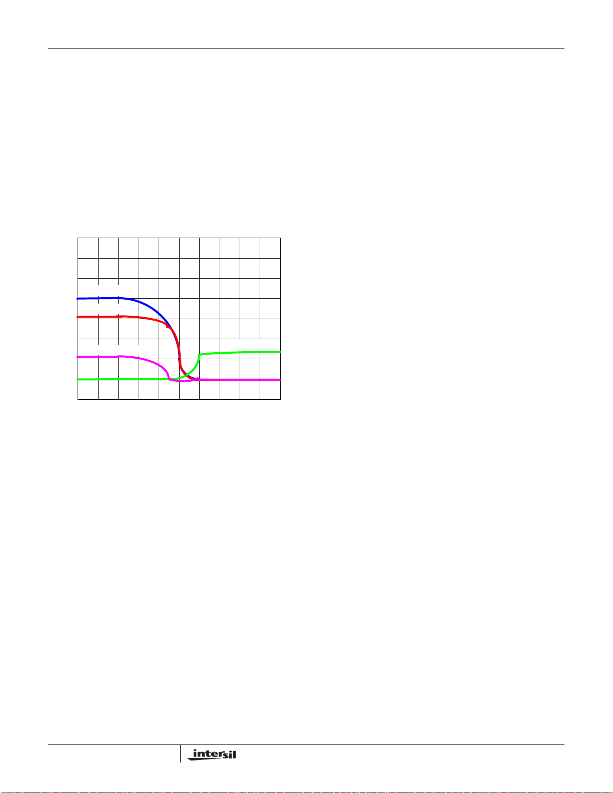
As referenced in the “Block Diagram” on page 2, the UGATE
signal is referenced to PHASE signal. The deadtime
comparator also looks at the difference (UGATE - PHASE).
This is significant when viewing the gate driver waveforms on
an oscilloscope. One simple indication of shoot-through (or
insufficient deadtime) is when the UGATE and LGA TE signals
overlap. But in this case, one should look at UGATE-PHASE
(either by a math function of the two signals, or by using a
differential probe measurement) compared to LGATE.
Figure 12 shows an example of this. It looks as if the UGATE
and LGA TE signal s have cro ssed, but the UGATE-PHASE
signal does not cross the LGA TE.
UGATE (4V/DIV)
PHASE (4V/DIV)
UGATE-PHASE (4V/DIV)
GND>
GND>
GND>
GND>
FIGURE 12. GATE DRIVER WAVEFORMS
LGATE (4V/DIV)
One important consideration is negative spikes on the PHASE
node as it goes low. The upper FET is turning of f, but before
the lower FET can take over , stray induct ance in the l ayout
(on the board, or even the inductance of some components,
such as D
2
P AK FETs) can contribute to the PHASE going
negative.
There is no maximum spec for PHASE spike below GND,
however, there is an absolute maximum rating fo r
(BOOT - PHASE) of 7V; exceeding this limit can cause
damage to the IC, and possibly to the system. Since the
BOOT signal is typically 5V above the PHASE node most of
the time, it only takes a few volts of a spike on either signal to
exceed the limit. A good design should be characterized by
using the math function or differen tial probe, an d monitoring
these signals for compliance, especially during full loads,
where the signals are usually the noisiest. Slowing down the
turn-off of the upper FET may help, while at other times,
sometimes the problem may just be the choice of FETs.
If the power efficiency of the system is important, then other
FET parameters are also considered. Efficiency is a measure
of power losses from input to output, and it contains two major
components: losses in the IC (mostly in the gate drivers) and
losses in the FETs. Optimizing the sum involves many
trade-offs (for example, raising the voltage of the gate drivers
typically adds power to the IC side, but may reduce some
power on the FET side). For low duty cycle applications (such
as 12V in to 1.5V out), the upper FET is usually chosen for low
gate charge, since switching losses are key , while the lower
FET is chosen for low R
, since it is on most of the time.
DS(ON)
For high duty cycles (such as 3.3V in to 2.5V out), the
opposite is true.
In summary , the fo llowing parameters may need to be
considered in choosing the right FETs for an application:
drain-source breakdown voltage rating, gate-source rating,
maximum current, thermal and package considerations, low
gate threshold voltage, gate charge, R
DS(ON)
at 4.5V, and
switching speed. And, of course, the board layout constraints
and cost also are factored into the decision.
Linear FET Considerations
The linear FET is chosen primarily for thermal performance.
The current for the linear output is generally limited by the
power dissipation (P = (V
thermal rating for getting the heat out of the package, and
spreading it out on the board, especially when no heat sinks or
airflow is available. It is generally not recommended to paralle l
two FETs in order to get higher current or to spread out the
heat, as the FETs would need to be very well-matched in
order to share the current properly . Should this approach be
desired, and as perfectly matched FETs are seldom available,
a small resistor, or PC B trace o f suit able resi st an ce placed in
the source of each of the FET s can be used to imp rove the
current balance.
The maximum V
OUT2
several factors:
• Power dissipation, as described earlier
• Input voltage available
• LDO_DR voltage
• FET chosen
The voltage cannot be any higher than the input voltage
available, and the max V
The LDO_DR voltage is driven from the VCC12 rail; allowing
for headroom, the typical maximum voltage is 11V (lower as
VCC12 goes to its minimum of 10.8V). So the maximum
output voltage will be at least a V
FET threshold voltage) below the 11V, at the maximum loa d
current; some additional headroom is usually needed to
handle transient conditions. So a practical typical value
around 8V may be possible, but remember to also factor in
the variations for worst case conditions on V
parameters. As long as the V
headroom versus VCC12 is not a problem, then the maximum
output voltage is just below V
at maximum current.
The input supply for V
less than 12V, subject to the considerations above. The
drain-source breakdown voltage of the FET should be greater
IN2
- V
) * I), and the FET
OUT2
voltage allowed is determined by
is 12V (13.2V for a ±10% supply).
IN2
drop (which includes the
GS
and the FET
is low enough such that
IN2
, based on the R
IN2
can also be any available supply
IN2
IN2
DS(ON)
drop
14
FN9168.2
September 22, 2006
Page 15
ISL6549
than the V
voltage. The FET’s gate-source rating should be
IN2
greater than 12V (even though the output voltage may not
require such a high gate voltage, load transients or other
disturbances might force LDO_DR to momentarily approach
12V). The FET threshold is not critical, except for the cases
where the LDO_DR headroom is diminished. And finally, the
package (and board area allowed) must be able to handle the
maximum power dissipation expected.
Application Guidelines
Layout Considerations
Layout is very important in high frequency switching converter
design. With power devices switching efficiently at 600kHz,
the resulting current transitions from one device to another
cause voltage spikes across the interconnecting impedances
and parasitic circuit elements. These voltage spikes can
degrade efficiency, radiate noise into the circuit, and lead to
device overvoltage stress. Careful component layout and
printed circuit board design minimizes the voltage spikes in
the converters.
As an example, consider the turn-off transition of the PWM
upper MOSFET. Prior to turn-off, the MOSFET is carrying the
full load current. During turn-off, current stops flowing in the
upper MOSFET and is picked up by the lower MOSFET and
parasitic diode. Any parasitic indu ct an ce i n the sw itch ed
current path generates a large voltage spike during the
switching interval. Careful component selection, tight layout of
the critical components, and short, wide traces minimizes the
magnitude of voltage spikes.
There are two sets of critical components in a DC/DC converter
using the ISL6549. The switching components are the most
critical because they switch large amounts of energy, and
therefore tend to generate large amounts of noise. Next are the
small signal components which connect to sensitive nodes or
supply critical bypass current and signal coupling.
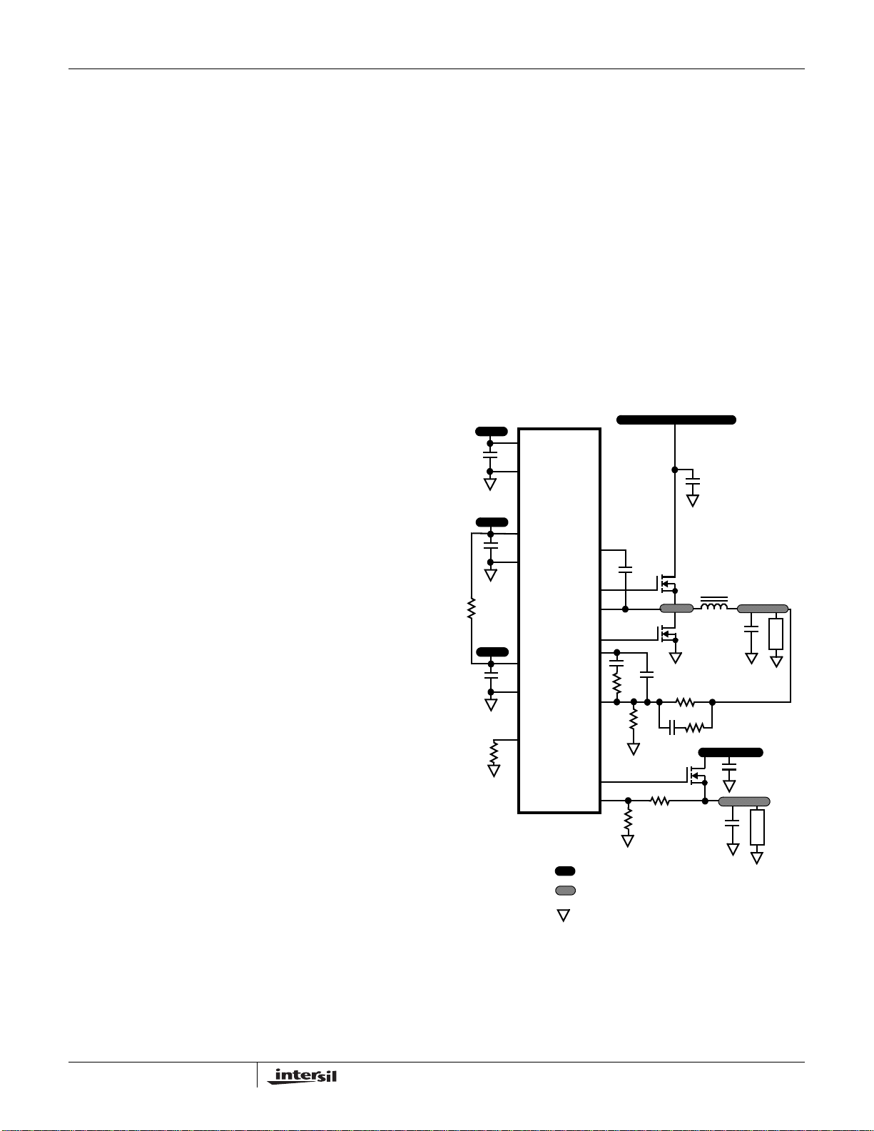
A multilayer printed circuit board is recommended. Figure 13
shows the connections of the critical components in the
converter. Capacitors C
numerous physical capacitors. Dedicate one solid layer,
usually a middle layer of the PC board, for a ground plane and
make all critical component ground connections through vias
to this layer. Dedicate another so lid laye r as a power pl ane
and break this plane into smaller islands of common voltage
levels. Keep the metal runs from the PHASE terminal to the
output inductor short. The power plane should support the
input and output power nodes. Use copper filled polygons on
the top and bottom circuit layers for the phase node. Use the
remaining printed circuit layers for small signal wiring. The
wiring traces from the LGATE and UGATE pins to the
MOSFET gates should be kept short and wide enough to
easily handle the several Amps of drive current.
The critical small signal components include any bypass
capacitors, feedback components, and compe nsation
and C
IN
could each represent
OUT
components. Position the bypass capacito rs, C
, C5, and C6
4
close to their pins with a local GND connection, or via directly
to the ground plane. R12 should be placed near VCC5 and
PVCC5 pins. FS_DIS resistor R7 should be near the FS-DIS
pin, and its GND return should be short, and kept away from
the noisy FET GND. Place the PWM converter compensation
components close to the FB and COMP pins. The feedback
resistors for both regulators should also be located as close
as possible to the relevant FB pin with vias tied straight to the
ground plane as required.
Then the switching components should be placed cl ose to the
ISL6549. Minimize the length of the connections between the
input capacitors, C
, and the power switches by placing them
IN
nearby . Position both the ceramic and bulk inpu t capacitors as
close to the upper MOSFET drain as possible, and make the
GND returns (from lower FET source to VIN cap GND) short.
Position the output inductor and output capacitors between
the upper MOSFET and lower MOSFET and the load.
V
VCC12
PVCC5
R12
VCC5
C
C
C
R
4
6
5
7
VCC12
GND
ISL6549
PVCC5
PGND
VCC5
GND
FS_DIS
BOOT
UGATE
PHASE
LGATE
COMP
FB
LDO_DR
LDO_FB
KEY
ISLAND ON POWER PLANE LAYER
ISLAND ON CIRCUIT PLANE LAYER
VIA CONNECTION TO GROUND PLANE
C
C
R
2
IN1
C
IN1
7
Q1
L
OUT
V
OUT1
Q2
C
OUT1
2
C
1
R1
C
R
3
R5
3
C
Q3
OUT2
V
IN2
R6
R
4
C
IN2
LOAD
V
LOAD
OUT2
FIGURE 13. PRINTED CIRCUIT BOARD POWER PLANES
AND ISLANDS
References
Applications Note: AN1201
Visit us on the internet: www.intersil.com
15
FN9168.2
September 22, 2006
Page 16
ISL6549
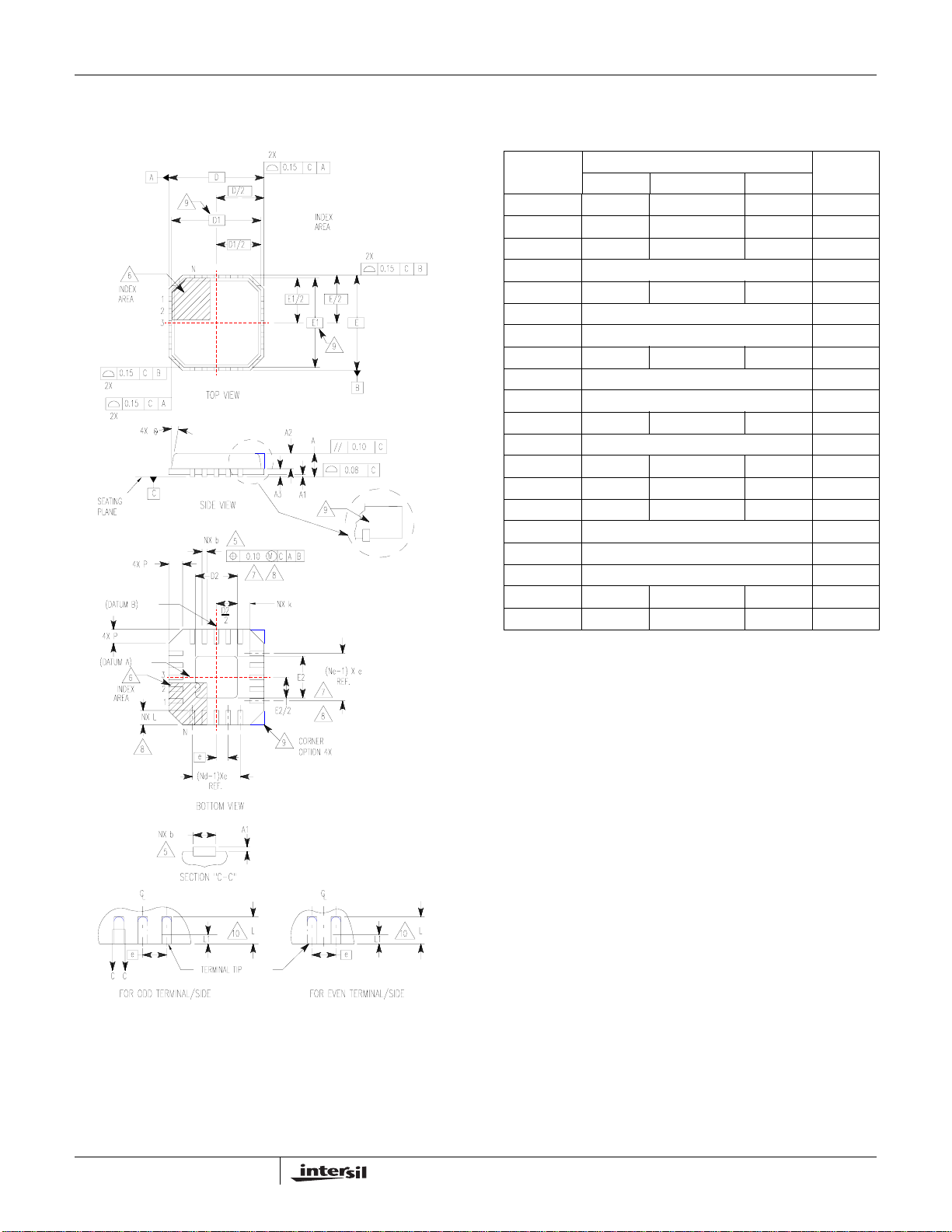
Quad Flat No-Lead Plastic Package (QFN)
Micro Lead Frame Plastic Package (MLFP)
L16.4x4
16 LEAD QUAD FLAT NO-LEAD PLASTIC PACKAGE
(COMPLIANT TO JEDEC MO-220-VGGC ISSUE C)
MILLIMETERS
SYMBOL
A 0.80 0.90 1.00 A1 - - 0.05 A2 - - 1.00 9
A3 0.20 REF 9
b 0.23 0.28 0.35 5, 8
D 4.00 BSC -
D1 3.75 BSC 9
D2 1.95 2.10 2.25 7, 8
E 4.00 BSC E1 3.75 BSC 9
E2 1.95 2.10 2.25 7, 8
e 0.65 BSC -
k0.25 - - -
L 0.50 0.60 0.75 8
L1 - - 0.15 10
N162
Nd 4 3
Ne 4 3
P- -0.609
θ --129
NOTES:
1. Dimensioning and tolerancing conform to ASME Y14.5-1994.
2. N is the number of terminals.
3. Nd and Ne refer to the number of terminals on each D and E.
4. All dimensions are in millimeters. Angles are in degrees.
5. Dimension b applies to the metallized terminal and is measured
between 0.15mm and 0.30mm from the terminal tip.
6. The configuration of the pin #1 identifier is optional, but must be
located within the zone indicated. The pin #1 identifier may be
either a mold or mark feature.
7. Dimensions D2 and E2 are for the exposed pads which provide
improved electrical and thermal performance.
8. Nominal dimensions are provided to assist with PCB Land Pattern
Design efforts, see Intersil Technical Brief TB389.
9. Features and dimensions A2, A3, D1, E1, P & θ are present when
Anvil singulation method is used and not present for saw
singulation.
10. Depending on the method of lead termination at the edge of the
package, a maximum 0.15mm pull back (L1) maybe present. L
minus L1 to be equal to or greater than 0.3mm.
NOTESMIN NOMINAL MAX
Rev. 5 5/04
16
FN9168.2
September 22, 2006
Page 17
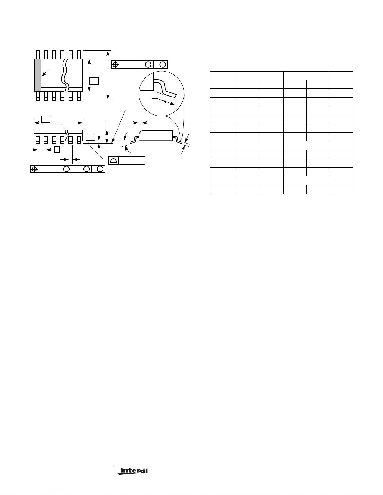
Small Outline Plastic Packages (SOIC)
ISL6549
N
INDEX
AREA
123
-A-
E
-B-
SEATING PLANE
D
A
-C-
0.25(0.010) BM M
H
L
h x 45
o
α
e
B
0.25(0.010) C AM BS
M
NOTES:
1. Symbols are defined in the “MO Series Symbol List” in Section 2.2 of
Publication Number 95.
2. Dimensioning and tolerancing per ANSI Y14.5M-1982.
3. Dimension “D” does not include mold flash, protrusions or gate burrs.
Mold flash, protrusion and gate burrs shall not exceed 0.15mm (0.006
inch) per side.
4. Dimension “E” does not include interlead flash or protrusions. Interlead
flash and protrusions shall not exceed 0.25mm (0.010 inch) per side.
5. The chamfer on the body is optional. If it is not present, a visual index
feature must be located within the crosshatched area.
6. “L” is the length of terminal for soldering to a substrate.
7. “N” is the number of terminal positions.
8. Terminal numbers are shown for reference only.
9. The lead width “B”, as measured 0.36mm (0.014 inch) or greater
above the seating plane, shall not exceed a maximum value of
0.61mm (0.024 inch).
10. Controlling dimension: MILLIMETER. Converted inch dimensions
are not necessarily exact.
A1
C
0.10(0.004)
M14.15 (JEDEC MS-012-AB ISSUE C)
14 LEAD NARROW BODY SMALL OUTLINE PLASTIC
PACKAGE
INCHES MILLIMETERS
SYMBOL
A 0.0532 0.0688 1.35 1.75 -
A1 0.0040 0.0098 0.10 0.25 -
B 0.013 0.020 0.33 0.51 9
C 0.0075 0.0098 0.19 0.25 D 0.3367 0.3444 8.55 8.75 3
E 0.1497 0.1574 3.80 4.00 4
e 0.050 BSC 1.27 BSC -
H 0.2284 0.2440 5.80 6.20 -
h 0.0099 0.0196 0.25 0.50 5
L 0.016 0.050 0.40 1.27 6
N14 147
o
α
0
o
8
o
0
o
8
Rev. 0 12/93
NOTESMIN MAX MIN MAX
-
17
FN9168.2
September 22, 2006
Page 18
ISL6549
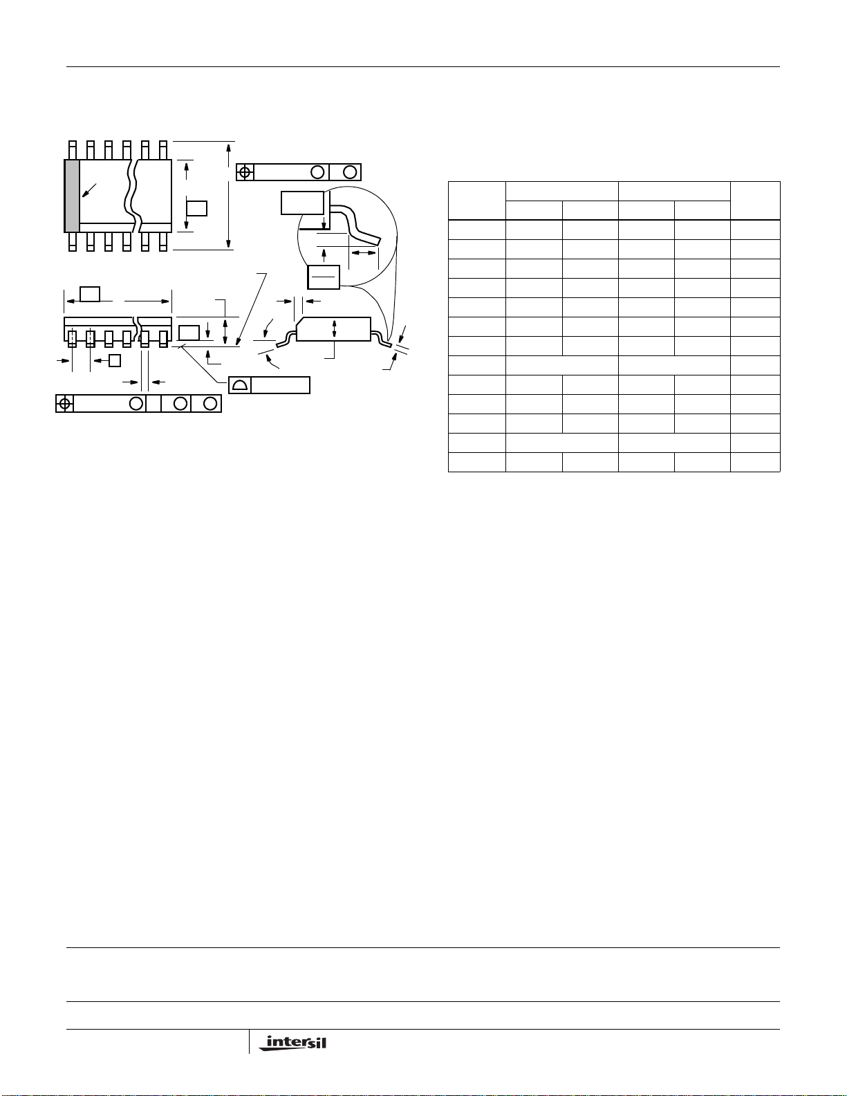
Shrink Small Outline Plastic Packages (SSOP)
Quarter Size Outline Plastic Packages (QSOP)
N
INDEX
AREA
123
-AD
e
B
0.17(0.007) C AMB
H
E
-B-
SEATING PLANE
A
-C-
A1
S
M
0.25(0.010) B
GAUGE
PLANE
α
0.10(0.004)
M
0.25
0.010
A2
M
h x 45°
NOTES:
1. Symbols are defined in the “MO Series Symbol List” in Section
2.2 of Publication Number 95.
2. Dimensioning and tolerancing per ANSI Y14.5M-1982.
3. Dimension “D” does not include mold flash, protrusions or gate
burrs. Mold flash, protrusion and gate burrs shall not exceed
0.15mm (0.006 inch) per side.
4. Dimension “E” does not include interlead flash or protrusions.
Interlead flash and protrusions shall not exceed 0.25mm (0.010
inch) per side.
5. The chamfer on the body is optional. If it is not present, a visual
index feature must be located within the crosshatched area.
6. “L” is the length of terminal for soldering to a substrate.
7. “N” is the number of terminal positions.
8. Terminal numbers are shown for reference only.
9. Dimension “B” does not include dambar protrusion. Allowable
dambar protrusion shall be 0.10mm (0.004 inch) total in excess
of “B” dimension at maximum material condition.
10. Controlling dimension: INCHES. Converted millimeter dimensions are not necessarily exact.
M16.15A
16 LEAD SHRINK SMALL OUTLINE PLASTIC PACKAGE
(0.150” WIDE BODY)
INCHES MILLIMETERS
SYMBOL
A 0.061 0.068 1.55 1.73 -
A1 0.004 0.0098 0.102 0.249 -
L
A2 0.055 0.061 1.40 1.55 -
B 0.008 0.012 0.20 0.31 9
C 0.0075 0.0098 0.191 0.249 D 0.189 0.196 4.80 4.98 3
E 0.150 0.157 3.81 3.99 4
C
e 0.025 BSC 0.635 BSC -
H 0.230 0.244 5.84 6.20 -
h 0.010 0.016 0.25 0.41 5
L 0.016 0.035 0.41 0.89 6
N16 167
α
0° 8° 0° 8° -
NOTESMIN MAX MIN MAX
Rev. 2 6/04
All Intersil U.S. products are manufactured, assembled and tested utilizing ISO9000 quality systems.
Intersil Corporation’s quality certifications can be viewed at www.intersil.com/design/quality
Intersil products are sold by description only. Intersil Corporation reserves the right to make changes in circuit design, software and/or specifications at any time without
notice. Accordingly, the reader is cautioned to verify that data sheets are current before placing orders. Information furnished by Intersil is believed to be accurate and
reliable. However, no responsibility is assumed by Intersil or its subsidiaries for its use; nor for any infringements of patents or other rights of third parties which may result
from its use. No license is granted by implicat ion or oth erwise u nde r any p a tent or p at ent r ights of Intersil or its subsidiaries.
For information regarding Intersil Corporation and its products, see www.intersil.com
18
FN9168.2
September 22, 2006
 Loading...