intersil ISL6545, ISL6545A DATA SHEET

®
ISL6545, ISL6545A
Data Sheet November 15, 2006
5V or 12V Single Synchronous Buck
Pulse-Width Modulation (PWM) Controller
The ISL6545 makes simple work out of implementing a
complete control and protection scheme for a DC/DC stepdown
converter driving N-channel MOSFETs in a synchronous buck
topology. Since it can work with either 5V or 12V supplies, this
one IC can be used in a wide variety of applications within a
system. The ISL6545 integrates the control, gate drivers, output
adjustment, monitoring and protection functions into a single 8
Ld SOIC or 10 Ld DFN package.
The ISL6545 provides single feedback loop, voltage-mode
control with fast transient response. The output voltage can be
precisely regulated to as low as 0.6V , with a maximum
tolerance of ±1.0% over temperature and line voltage
variations. A selectable fixed frequency oscillator (ISL6545 for
300kHz; ISL6545A for 600kHz) reduces design complexity,
while balancing typical application cost and efficiency.
The error amplifier features a 20MHz gain-bandwidth
product and 9V/μs slew rate which enables high converter
bandwidth for fast transient performance. The resulting
PWM duty cycles range from 0% to 100%.
Protection from overcurrent conditions is provided by
monitoring the r
operation appropriately. This approach simplifies the
implementation and improves efficiency by eliminating the
need for a current sense resistor.
of the lower MOSFET to inhibit PWM
DS(ON)
FN6305.3
Features
• Operates from +5V or +12V Supply Voltage (for bias)
- 1.0V to 12V V
Input Range (up to 20V possible with
IN
restrictions; see Input Voltage Considerations)
- 0.6V to V
- Integrated Gate Drivers use V
Output Range
IN
(5V to 12V)
CC
- 0.6V Internal Reference; ±1.0% tol erance
• Simple Single-Loop Control Design
- Voltage-Mode PWM Control
- Drives N-Channel MOSFETs
• Fast Transient Response
- High-Bandwidth Error Amplifier
- Full 0% to 100% Duty Cycle
• Lossless, Programmable Overcurrent Protection
- Uses Lower MOSFET’s r
DS(ON)
• Small Converter Size in 8 Ld SOIC or 10 Ld DFN
- 300kHz or 600kHz Fixed Frequency Oscillator
- Fixed Internal Soft-Start, Capable into a Pre-biased
Load
- Integrated Boot Diode
- Enable/Shutdown Function on COMP/SD Pin
- Output Current Sourcing and Sinking
• Pb-Free Plus Anneal Available (RoHS Compliant)
Applications
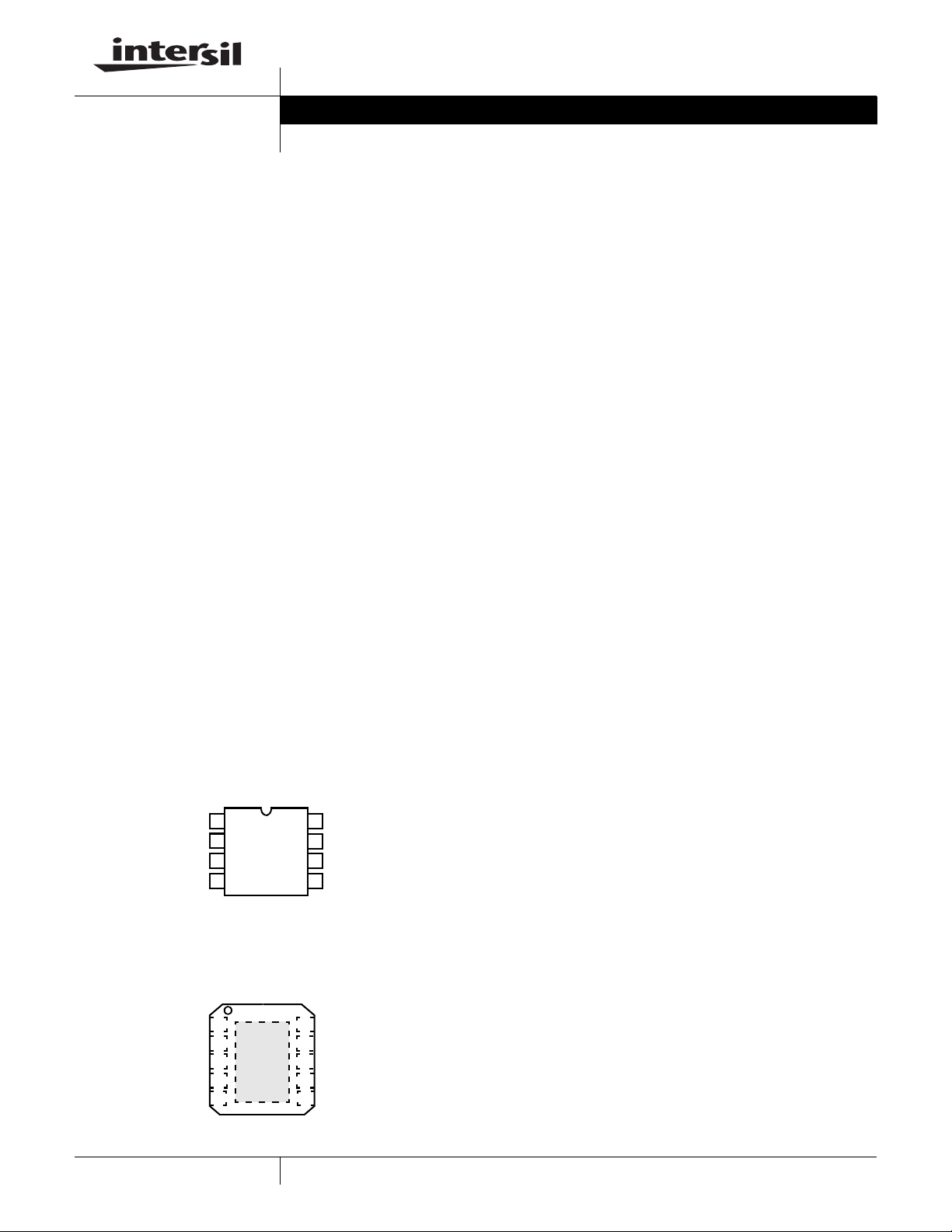
Pinout
BOOT
UGATE
GND
LGATE/OCSET
ISL6545 (10 LD 3x3 DFN)
BOOT
UGATE
N/C
GND
LGATE/OCSET
ISL6545 (SOIC)
TOP VIEW
1
2
3
4
TOP VIEW
1
2
GND
3
4
5
1
8
7
6
5
10
9
8
7
6
PHASE
COMP/SD
FB
VCC
PHASE
COMP/SD
FB
N/C
VCC
• Power Supplies for Microprocessors or Peripherals
- PCs, Embedded Controllers, Memory Supplies
- DSP and Core Communications Processor Supplies
• Subsystem Power Supplies
- PCI, AGP; Graphics Cards; Digital TV
- SSTL-2 and DDR/DDR2/DDR3 SDRAM Bus
Termination Supply
• Cable Modems, Set Top Boxes, and DSL Modems
• Industrial Power Supplies; General Purpose Supplies
• 5V or 12V-Input DC/DC Regulators
• Low-Voltage Distributed Power Supplies
CAUTION: These devices are sensitive to electrostatic discharge; follow proper IC Handling Procedures.
1-888-INTERSIL or 1-888-468-3774
| Intersil (and design) is a registered trademark of Intersil Americas Inc.
All other trademarks mentioned are the property of their respective owners.
Copyright © Intersil Americas Inc. 2006. All Rights Reserved

ISL6545, ISL6545A
*
Ordering Information
TEMP.
PAR T NUMB ER PART M ARKI NG
ISL6545CBZ* (300kHz) 6545 CBZ 0 to +70 8 Ld SOIC (Pb-free) M8.15
ISL6545ACBZ*(600kHz)
6545 ACBZ 0 to +70 8 Ld SOIC (Pb-free) M8.15
(Note)
ISL6545IBZ* (300kHz)
6545 IBZ -40 to +85 8 Ld SOIC (Pb-free) M8.15
(Note)
ISL6545AIBZ* (600kHz)
6545 AIBZ -40 to +85 8 Ld SOIC (Pb-free) M8.15
(Note)
ISL6545CRZ* (300kHz)
545Z 0 to +70 10 Ld DFN (Pb-free) L10.3x3C
(Note)
ISL6545ACRZ* (600kHz)
45AZ 0 to +70 10 Ld DFN (Pb-free) L10.3x3C
(Note)
ISL6545IRZ* (300kHz)
45IZ -40 to +85 10 Ld DFN (Pb-free) L10.3x3C
(Note)
ISL6545AIRZ* (600kHz)
5ARZ -40 to +85 10 Ld DFN (Pb-free) L10.3x3C
(Note)
ISL6545EVAL1 Evaluation Board (SO-8)
ISL6545AEVAL1 Evaluation Board (SO-8)
*Add “-T” suffix for tape and reel.
NOTE: Intersil Pb-free plus anneal products employ special Pb-free material sets; molding compounds/die attach materials and 100% matte tin plate
termination finish, which are RoHS compliant and compatible with both SnPb and Pb-free soldering operations. Intersil Pb-free products are MSL
classified at Pb-free peak reflow temperatures that meet or exceed the Pb-free requirements of IPC/JEDEC J STD-020.
RANGE (°C) PACKAGE PKG. DWG. #
2
FN6305.3
November 15, 2006

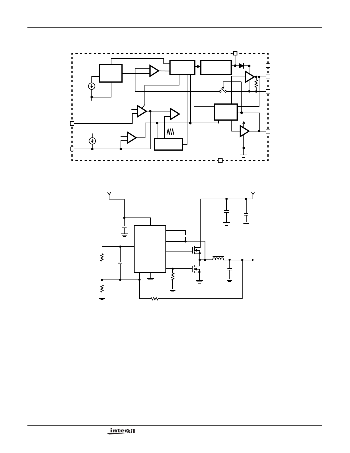
Block Diagram
LGATE/OCSET
FB
COMP/SD
Typical Application
21.5μA
TO
5V int.
20μA
SAMPLE
AND
HOLD
0.6V
0.4V
ISL6545, ISL6545A
+
OC
COMPARATOR
ERROR
AMP
DIS
+
-
+
-
FIXED 300 (or 600)kHz
PWM
COMPARATOR
OSCILLATOR
POR AND
SOFT-START
+
-
INTERNAL
REGULATOR
5V int.
INHIBIT
PWM
CONTROL
LOGIC
DIS
GND
GATE
VCC
D
BOOT
VCC
20kΩ
BOOT
UGATE
PHASE
LGATE/OCSET
R
OFFSET
R
F
C
F
V
CC
5V or 12V
C
DCPL
COMP/SD
C
I
Type II
compensation
shown
ISL6545
7
63
FB
5
VCC
GND
R
S
1
8
BOOT
PHASE
UGATE
2
LGATE/OCSET
4
R
OCSET
C
BOOT
L
OUT
C
OUT
V
IN
1V-12V
C
+V
BULK
O
C
HF
3
FN6305.3
November 15, 2006

ISL6545, ISL6545A
Absolute Maximum Ratings Thermal Information
Supply Voltage, VCC . . . . . . . . . . . . . . . . . . . . . GND - 0.3V to 15V
BOOT Voltage, V
UGATE Voltage V
LGATE/OCSET Voltage, V
PHASE Voltage, V
Upper Driver Supply Voltage, V
Clamp Voltage, V
FB, COMP/SD Voltage. . . . . . . . . . . . . . . . . . . . . .GND - 0.3V to 6V
. . . . . . . . . . . . . . . . . . . .GND - 0.3V to 36V
BOOT
. . . . . . . .V
UGATE
LGATE/OCSET
. . . . . . . . . .GND - 0.3V to V
PHASE
BOOT
BOOT
- VCC . . . . . . . . . . . . . . . . . . . . . . . . . . .24V
- 0.3V to V
PHASE
GND - 0.3V to VCC + 0.3V
- V
. . . . . . . . . . . . .15V
PHASE
BOOT
BOOT
+ 0.3V
+ 0.3V
ESD Classification, HBM . . . . . . . . . . . . . . . . . . . . . . . . . . . . . 1.5kV
ESD Classification, MM . . . . . . . . . . . . . . . . . . . . . . . . . . . . . . .150V
ESD Classification, CDM. . . . . . . . . . . . . . . . . . . . . . . . . . . . . 1.0kV
Operating Conditions
Supply Voltage, VCC . . . . +5V ±10%, +12V ±20%, or 6.5V to 14.4V
Ambient Temperature Range
ISL6545C, ISL6545AC. . . . . . . . . . . . . . . . . . . . . . . 0°C to +70°C
ISL6545I, ISL6545AI . . . . . . . . . . . . . . . . . . . . . . .-40°C to +85°C
Junction Temperature Range. . . . . . . . . . . . . . . . . .-40°C to +125°C
CAUTION: Stresses above those listed in “Absolute Maximum Ratings” may cause permanent damage to the device. This is a stress only rating and operation of the
device at these or any other conditions above those indicated in the operational sections of this specification is not implied.
NOTES:
is measured with the component mounted on a high effective thermal conductivity test board in free air. See Tech Brief TB379 for details.
1. θ
JA
is measured with the component mounted on a high effective thermal conductivity test board in free air, with “direct attach” features. See
2. θ
JA
Tech Brief TB379 for details.
3. For θ
4. Guaranteed by design; not production tested
, the “case temp” location is the center of the exposed metal pad on the package underside.
JC
Thermal Resistance θ
(°C/W) θJC (°C/W)
JA
SOIC Package (Note 1) . . . . . . . . . . . . 95 N/A
DFN Package (Note 3). . . . . . . . . . . . . 44 5.5
Maximum Junction Temperature
(Plastic Package) . . . . . . . . . . . . . . . . . . . . . . . . . . . . . . . . +150°C
Maximum Storage Temperature Range. . . . . . . . . -65°C to +150°C
Maximum Lead Temperature
(Soldering 10s) . . . . . . . . . . . . . . . . . . . . . . . . . . . . . . . . . . +300°C
(SOIC - Lead Tips Only)
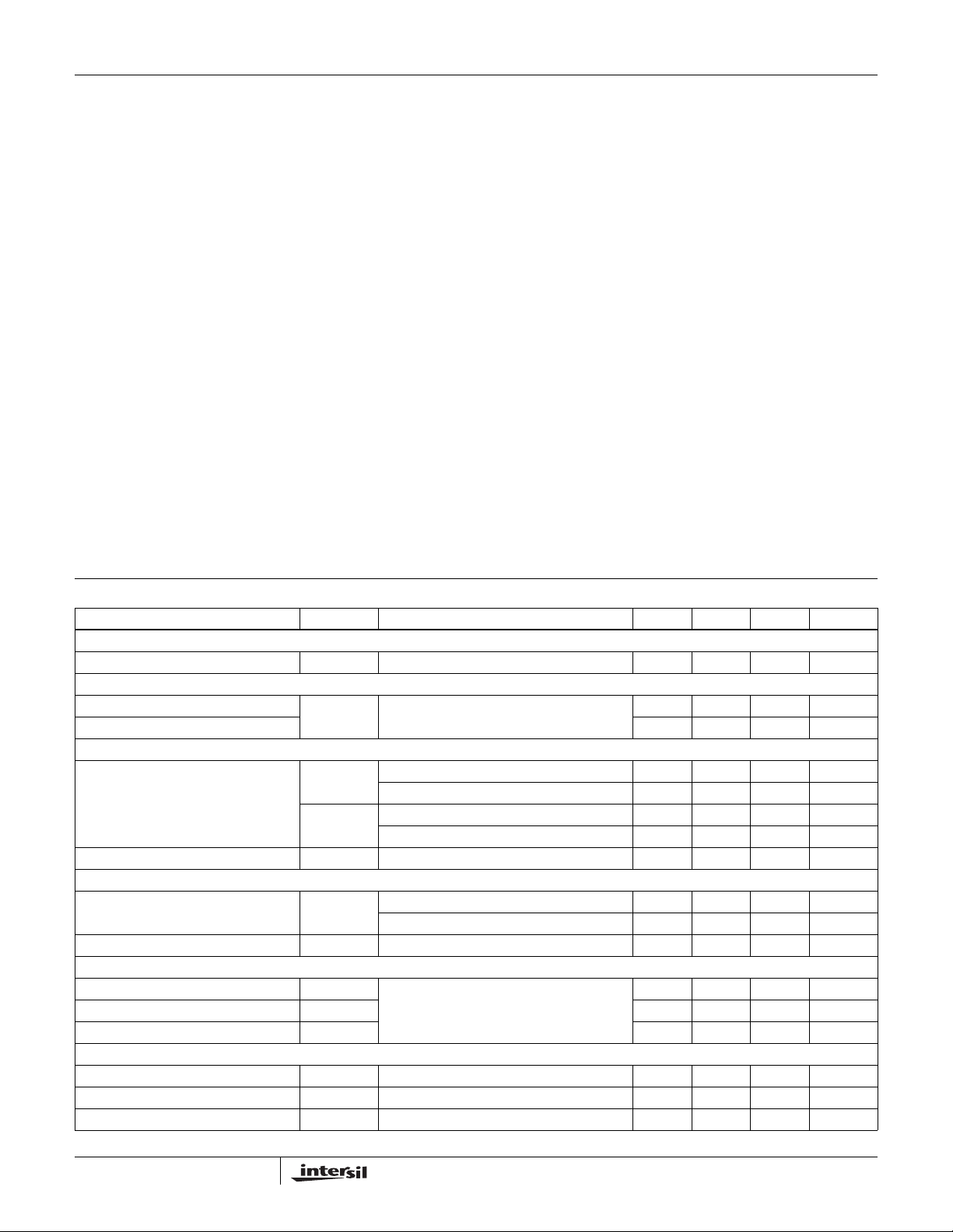
Electrical Specifications Test Conditions: V
= 12V, TJ = 0 to 85°C, Unless Otherwise Noted.
CC
PARAMETER SYMBOL TEST CONDITIONS MIN TYP MAX UNITS
SUPPLY CURRENT
V
CC
Input Bias Supply Current I
VCC
VCC = 12V; disabled 4 5.2 7 mA
POWER-ON RESET
Rising V
V
CC
POR Threshold V
CC
POR
POR Threshold Hysteresis 0.30 0.35 0.40 V
3.9 4.1 4.3 V
OSCILLATOR
Switching Frequency f
OSC
ISL6545C 270 300 330 kHz
ISL6545I 240 300 330 kHz
f
OSC
ISL6545AC 540 600 660 kHz
ISL6545AI 510 600 660 kHz
Ramp Amplitude (Note 4) ΔV
OSC
1.5 V
REFERENCE
Reference Voltage Tolerance ISL6545C -1.0 - +1.0 %
ISL6545I -1.5 - +1.5 %
Nominal Reference Voltage V
REF
0.600 V
ERROR AMPLIFIER
DC Gain (Note 4) GAIN - 96 - dB
Gain-Bandwidth Product (Note 4) GBWP - 20 - MHz
Slew Rate (Note 4) SR - 9 - V/μs
GATE DRIVERS
Upper Gate Source Impedance R
Upper Gate Sink Impedance R
Lower Gate Source Impedance R
UG-SRChVCC
UG-SNKhVCC
LG-SRChVCC
= 14.5V; I = 50mA - 3.0 - Ω
= 14.5V; I = 50mA - 2.7 - Ω
= 14.5V; I = 50mA - 2.4 - Ω
P-P
4
FN6305.3
November 15, 2006

ISL6545, ISL6545A
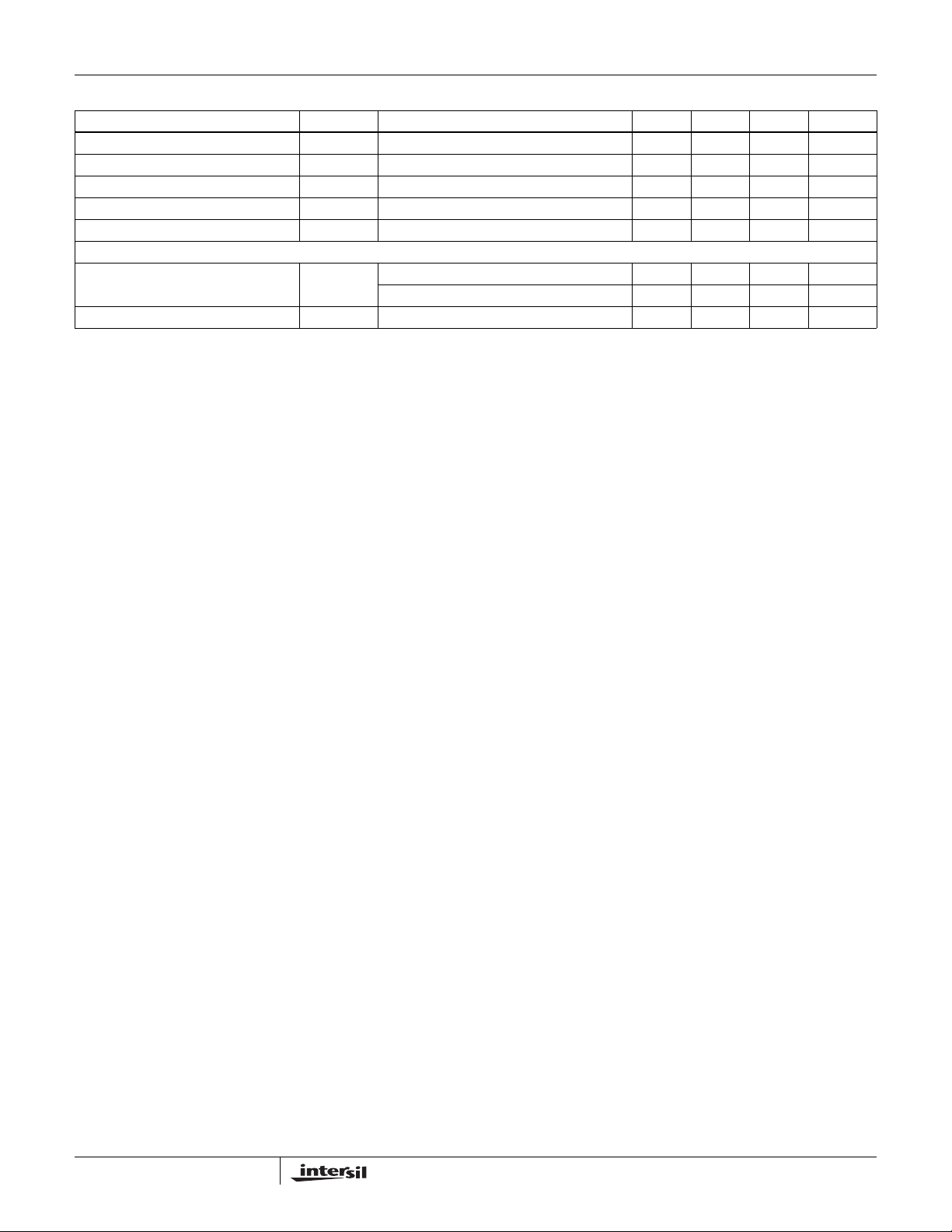
Electrical Specifications Test Conditions: V
PARAMETER SYMBOL TEST CONDITIONS MIN TYP MAX UNITS
Lower Gate Sink Impedance R
Upper Gate Source Impedance R
Upper Gate Sink Impedance R
Lower Gate Source Impedance R
Lower Gate Sink Impedance R
PROTECTION/DISABLE
OCSET Current Source I
Disable Threshold (COMP/SD pin) V
LG-SNKhVCC
UG-SRClVCC
UG-SNKlVCC
LG-SRClVCC
LG-SNKlVCC
OCSET
DISABLE
= 12V, TJ = 0 to 85°C, Unless Otherwise Noted. (Continued)
CC
= 14.5V; I = 50mA - 2.0 - Ω
= 4.25V; I = 50mA - 3.5 - Ω
= 4.25V; I = 50mA - 2.7 - Ω
= 4.25V; I = 50mA - 2.75 - Ω
= 4.25V; I = 50mA - 2.1 - Ω
ISL6545C; LGATE/OCSET = 0V 19.5 21.5 23.5 μA
ISL6545I; LGATE/OCSET = 0V 18.0 21.5 23.5 μA
Functional Pin Description (SOIC,DFN)
VCC (SOIC Pin 5, DFN Pin 6)
This pin provides the bias supply for the ISL6545, as well as
the lower MOSFET’s gate, and the BOOT voltage for the
upper MOSFET’s gate. An internal 5V regulator will supply
bias if V
BOOT will still be sourced by VCC). Connect a welldecoupled 5V or 12V supply to this pin.
FB (SOIC Pin 6, DFN Pin 8)
This pin is the inverting input of the internal error amplifier. Use
FB, in combination with the COMP/SD pin, to compensate the
voltage-control feedback loop of the converter. A resistor divider
from the output to GND is used to set the regulation voltage.
GND (SOIC Pin 3, DFN Pin 4)
This pin represents the signal and power ground for the IC.
Tie this pin to the ground island/plane through the lowest
impedance connection available. For the DFN package, Pin
4 MUST be connected for electrical GND; the metal pad
under the package should also be connected to the GND
plane for thermal conductivity.
PHASE (SOIC Pin 8, DFN Pin 10)
Connect this pin to the source of the upper MOSFET, and
the drain of the lower MOSFET. It is used as the sink for the
UGATE driver, and to monitor the voltage drop across the
lower MOSFET for overcurrent protection. This pin is also
monitored by the adaptive shoot-through protection circuitry
to determine when the upper MOSFET has turned off.
UGATE (SOIC Pin 2, DFN Pin 2)
Connect this pin to the gate of upper MOSFET; it provides
the PWM-controlled gate drive. It is also monitored by the
adaptive shoot-through protection circuitry to determine
when the upper MOSFET has turned off.
BOOT (SOIC Pin 1, DFN Pin 1)
This pin provides ground referenced bias voltage to the upper
MOSFET driver. A bootstrap circuit is used to create a voltage
suitable to drive an N-channel MOSFET (equal to V
the on-chip BOOT diode voltage drop), with respect to PHASE.
rises above 6.5V (but the LGATE/OCSET and
CC
CC
minus
0.375 0.400 0.425 V
COMP/SD (SOIC Pin 7, DFN Pin 9)
This is a multiplexed pin. During soft-start and normal converter
operation, this pin represents the output of the error amplifier.
Use COMP/SD, in combination with the FB pin, to compensate
the voltage-control feedback loop of the converter.
Pulling COMP/SD low (V
DISABLE
= 0.4V nominal) will
shut-down (disable) the controller, which causes the
oscillator to stop, the LGATE and UGATE outputs to be held
low, and the soft-start circuitry to re-arm. The external pulldown device will initially need to overcome up to 5mA of
COMP/SD output current. However, once the IC is disabled,
the COMP output will also be disabled, so only a 20µA
current source will continue to draw current.
When the pull-down device is released, the COMP/SD pin
will start to rise, at a rate determined by the 20µA charging
up the capacitance on the COMP/SD pin. When the
COMP/SD pin rises above the V
DISABLE
trip point, the
ISL6545 will begin a new Initialization and soft-start cycle.
LGATE/OCSET (SOIC Pin 4, DFN Pin 5)
Connect this pin to the gate of the lower MOSFET; it provides
the PWM-controlled gate drive (from V
). This pin is also
CC
monitored by the adaptive shoot-through protection circuitry to
determine when the lower MOSFET has turned off.
During a short period of time following Power-On Reset
(POR) or shut-down release, this pin is also used to
determine the overcurrent threshold of the converter.
Connect a resistor (R
) from this pin to GND. See the
OCSET
Overcurrent Protection section for equations. An
overcurrent trip cycles the soft-start function, after two
dummy soft-start time-outs. Some of the text describing the
LGATE function may leave off the OCSET part of the name,
when it is not relevant to the discussion.
N/C (DFN only; Pin 3, Pin 7)
These two pins in the DFN package are No Connect.
5
FN6305.3
November 15, 2006
 Loading...