®
www.BDTIC.com/Intersil
ISL65426MREP
FN6575.0Data Sheet October 29, 2007
Enhanced Product (EP) 6.0A Dual
Synchronous Buck Regulator with
Integrated MOSFETs
The ISL65426MREP is a high efficiency dual output
monolithic synchronous buck converter operating over an
input voltage range of 2.5V to 5.5V. This single chip power
solution provides two output voltages which are selectable or
externally adjustable from 1.2V to 80% of the supply voltage
while delivering up to 6.0A of total combined output current
when used at T
synchronized 180° out of phase reducing the RMS input
current and ripple voltage.
The ISL65426MREP switches at a fixed frequency of 1MHz
and utilizes current-mode control with integrated
compensation to minimize the size and number of external
components. The internal synchronous power switches are
optimized for good thermal performance, high efficiency,
and eliminate the need for an external Schottky diode.
A unique power block architecture allows partitioning to
support one of four configuration options. One master
power block is associated with each synchronous converter
channel. Four floating slave power blocks allow the user to
assign them to either channel. Proper external
configuration of the power blocks is verified internally prior
to soft-start initialization.
Independent enable inputs allow for synchronization or
sequencing soft-start intervals of the two converter
channels. A third enable input allows additional sequencing
for multi-input bias supply designs. Individual power good
indicators (PG1, PG2) signal when output voltage is within
regulation window.
The ISL65426MREP integrates protection for both
synchronous buck regulator channels. The fault conditions
include overcurrent, undervoltage, and IC thermal monitor.
High integration contained in a thin Quad Flat No-lead
(QFN) package makes the ISL65426MREP an ideal choice
to power many of today’s small form factor applications. A
single chip solution for large scale digital ICs, like field
programmable gate arrays (FPGA), requiring separate core
and I/O voltages.
of +125°C or less. The two PWMs are
J
Device Information
The specifications for an Enhanced Product (EP) device are
defined in a Vendor Item Drawing (VID), which is controlled
by the Defense Supply Center in Columbus (DSCC). “Hotlinks” to the applicable VID and other supporting application
information are provided on our website.
Features
• Specifications per DSCC VID V62/07639
• Full Mil-Temp Electrical Performance from -55°C to +125°C
• Controlled Baseline with One Wafer Fabrication Site and
One Assembly/Test Site
• Full Homogeneous Lot Processing in Wafer Fab
• Current Density Validated per MIL-PRF-38535
• Full Traceability Through Assembly and Test by
Date/Trace Code Assignment
• Enhanced Process Change Notification
• Enhanced Obsolescence Management
• Eliminates Need for Up-Screening a COTS Component
• High Efficiency of up to 90%
• Fixed Frequency: 1MHz
• Operates From 2.5V to 5.5V Supply
• ±2.0% Reference
• Flexible Output Voltage Options
- Programmable 2-Bit VID Input
- Adjustable Output From 1.2V to 4.0V
• Power Blocks are Rated at:
- 1A typ for TJ < +125°C and VIN Range 4.0V to 5.5V
- 0.7A typ for TJ < +125°C and VIN Range 2.5V to 5.5V
• Ultra-Compact DC/DC Converter Design
• PWMs Synchronized 180
• Independent Enable Inputs and System Enable
• Independent Output Digital Soft-Start
• Power Good Output Voltage Monitor
• Short-Circuit and Thermal-Overload Protection
• Overcurrent and Undervoltage Protection
° Out of Phase
Applications
• FPGA, CPLD, DSP, and CPU Core and I/O Voltages
• Point-of-Load Regulation in Distributed Power Systems
Ordering Information
VENDOR PART
NUMBER
(Notes 1, 2)
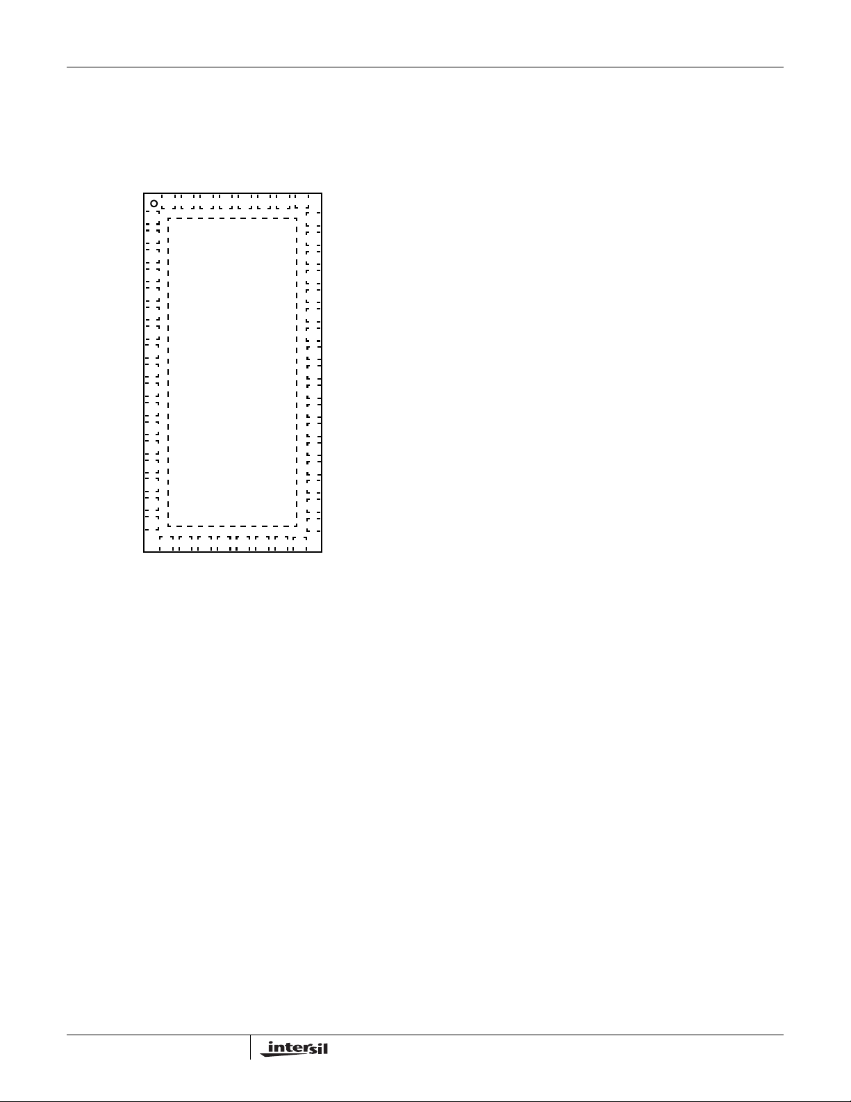
ISL65426MREP V62/07639-01XB -55 to +125 50 Ld 5x10
NOTES:
1. Add -TK suffix for 1000 piece tape and reel. Please refer to TB347 for
details on reel specifications.
2. Devices must be procured to the VENDOR PART NUMBER.
VENDOR ITEM
DRAWING
TEMP.
RANGE
(°C) PACKAGE
QFN
PKG.
DWG. #
L50.5x10
1
CAUTION: These devices are sensitive to electrostatic discharge; follow proper IC Handling Procedures.
1-888-INTERSIL or 1-888-468-3774
| Intersil (and design) is a registered trademark of Intersil Americas Inc.
All other trademarks mentioned are the property of their respective owners.
Copyright © Intersil Americas Inc. 2007. All Rights Reserved

Pinout
www.BDTIC.com/Intersil
PGND
PGND
PGND
PGND
LX1
LX1
PVIN1
PVIN2
LX2
PGND
PGND
LX3
PVIN3
VCC
VCC
VCC
PGND
ISL65426MREP
(50 LD QFN)
TOP VIEW
EN2
EN
EN1
FB1
50 49 48 47 46 45 44
1
2
3
4
5
6
7
8
9
10
11
12
13
14
15
16
17
18 19 20 21 22 23 24
PGND
ISET2
ISL65426MREP
PG2
FB2
PG1
43
PGND
42
PGND
41
PGND
40
PGND
39
LX6
38
37
LX6
36
PVIN6
PVIN5
35
34
LX5
PGND
33
PGND
32
31
LX4
30
PVIN4
PGND
29
28
PGND
GND
27
GND
26
25
PGND
V1SET1
V1SET2
ISET1
V2SET1
V2SET2
PGND
PGND
2
FN6575.0
October 29, 2007

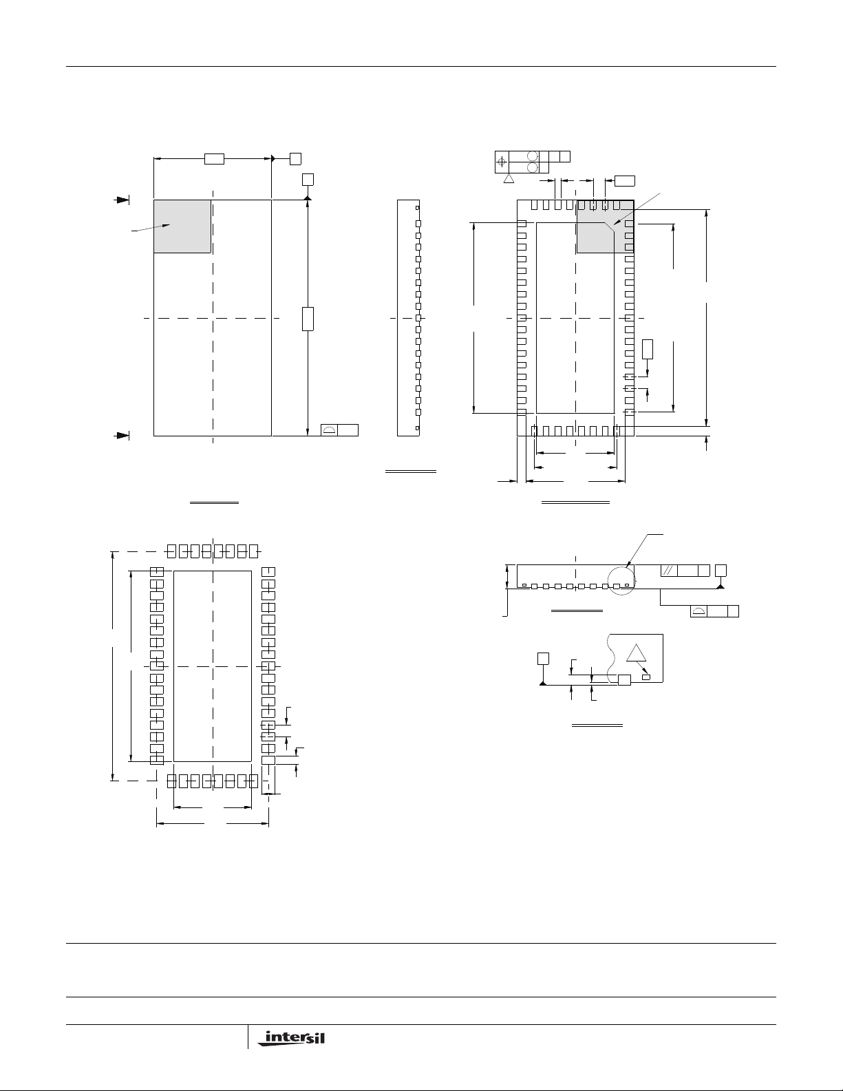
L50.5x10
www.BDTIC.com/Intersil
50 LEAD QUAD FLAT NO-LEAD PLASTIC PACKAGE
Rev 0, 7/06
ISL65426MREP
A
PIN 1
INDEX AREA
A
5.00
TOP VIEW BOTTOM VIEW
A
B
10.00
0.15
(4X)
VIEW "A-A"
0.40±0.10
0.10 M C A B
MC
0.05
4
0.25
42
8.10
26 17
25
3.30
0.50x7=3.50 REF
4.20
5043
0.50
18
PIN 1 INDEX AREA
(C 0.40)
1
0.50
9.20
0.50x16=8.00 REF
0.40±0.10
SEE DETAIL "X"
C
C
0.10
5
SEATING PLANE
ANGULAR ±2×
0.08 C
9.80
8.10
RECOMMENDED LAND PATTERN
3.30
4.80
(46 x 0.50)
(50 x 0.25)
(50 x 0.60)
MAX. 1.00
NOTES:
1. CONTROLLING DIMENSIONS ARE IN MM.
2. UNLESS OTHERWISE SPECIFIED TOLERANCE : DECIMAL ±0.05
3. DIMENSIONING AND TOLERANCE PER ASME Y 14.5M-1994.
4. DIMENSION LEAD WIDTH APPLIES TO THE PLATED TERMINAL
AND IS MEASURED BETWEEN 0.23MM AND 0.28MM FROM
THE TERMINAL TIP.
5. TIEBAR SHOWN (if present) IS A NON-FUNCTIONAL FEATURE
SIDE VIEW
C
0.2 REF
0.00 MIN.
0.05 MAX.
DETAIL "X"
All Intersil U.S. products are manufactured, assembled and tested utilizing ISO9000 quality systems.
Intersil Corporation’s quality certifications can be viewed at www.intersil.com/design/quality
Intersil products are sold by description only. Intersil Corporation reserves the right to make changes in circuit design, software and/or specifications at any time without
notice. Accordingly, the reader is cautioned to verify that data sheets are current before placing orders. Information furnished by Intersil is believed to be accurate and
reliable. However, no responsibility is assumed by Intersil or its subsidiaries for its use; nor for any infringements of patents or other rights of third parties which may result
from its use. No license is granted by implic atio n or other wise u nde r any p a tent or patent rights of Intersil or its subsidiaries.
For information regarding Intersil Corporation and its products, see www.intersil.com
3
FN6575.0
October 29, 2007
 Loading...