

Page 1
1
®
AN1021
CAUTION: These devices are sensitive to electrostatic discharge; follow proper IC Handling Procedures.
1-888-INTERSIL or 321-724-7143
| Intersil (and design) is a registered trademark of Intersil Americas Inc.
Copyright © Intersil Americas Inc. 2002. All Rights Reserved
PRELIMINARY
Embedded DC-DC Converters Using ISL6526 and
ISL6527 PWM Controller ICs
Introduction
The ISL6526 and the ISL6527 provide power control and
protection for applications requiring low voltage and high
power. Both ICs can be biased from voltages between 3.3V
and 5V. The ISL6526 and ISL6527 contain a high
performance error amplifier, a high accuracy reference, a
fixed 300kHz or 600kHz internal oscillator, over-current
protection circuitry, and two MOSFET drivers for use in
synchronous-rectified buck converters. Both the ISL6526
and the ISL6527 are capable of regulating the output voltage
while the DC-DC converter is sinking current. The ISL6527
also allows for an external reference to be used. All these
features are packaged in a small 14-lead SOIC or a 16-lead
5x5[mm] MLFP. More complete descriptions of the ISL6526
and the ISL6527 can be found in their respective
datasheets [1, 2].
This application note details the ISL6526 and ISL6527 in
DC-DC converters for applications requiring a tightly
regulated, fixed output voltage. Low-cost applications
requiring a DC-DC converter can benefit from one of the
designs presented in this application note
ISL6526/27 Reference Designs
The ISL6526/27 evaluation board highlights the operation of
the ISL6526 and ISL6527 ICs in an embedded application.
There are five evaluation boards from which to choose.
The ISL6526EVAL1 board is built with the ISL6526CB and
shipped with an ISL6526ACB sample piece. Evaluation of
the ISL6526CB can be performed immediately. If evaluation
of the ISL6526ACB is desired, then it is a simple matter of
replacing the controller. The ISL6527EVAL1 is shipped with
the ISL6527CB and shipped with an ISL6527ACB sample
piece. As with the ISL6526CB and ISL6526ACB, the parts
are interchangeable.
The ISL6526EVAL2 and ISL6527EVAL2 are ready for
evaluation without any modifications.
All evaluation boards have the same output filter,
compensation components and MOSFETs. They are
configured for an output of 2.5V with a maximum load of 5A.
The ISL6526 evaluation boards have a fixed output while the
ISL6527 evaluation boards allow the use of a potentiometer
to adjust the output voltage from 0.75V to 3.0V. Unless
otherwise noted, this application note assumes that the
output of the ISL6527 evaluation board is 2.5V.
Quick Start Evaluation
The evaluation board is shipped ‘ready to use’ right from the
box. The board accepts a range of input voltages from 3.3V
to 5V from a standard power supply. The output can be
exercised through an external load.
There are posts available on the board for introducing power
to the board and also for drawing current from the regulated
output. Three probe points are also available for use. These
probe points provide Kelvin connections to the
CPVOUT(TP3) and CT1(TP1) pins on both the ISL6526 and
ISL6527. The ENABLE pin on the ISL6526 and the REF_IN
pin on the ISL6527 can be probed from TP2.
Recommended Test Equipment
To test the functionality of the ISL6526 or ISL6527, the
following equipment is recommended:
- An adjustable 0 - 5V, 5A capable bench power supply
- An electronic load
- Four channel oscilloscope with probes
- Precision digital multimeter
Power and Load Connections
There are 2 sets of terminals that are used to supply the
input voltage and load the output.
INPUT VOLTAGE
Connect the positive lead of the adjustable bench power
supply to the 3.3V post (J1). Connect the ground lead of
the supply to GND post (J2).
OUTPUT LOADING - SOURCING CURRENT
Connect the positive terminal of the load to the VOUT
post (J3). Connect the return terminal of the same load to
the GND post (J4).
OUTPUT LOADING - SINKING CURRENT
CAUTION: The return terminal of the load must float for
this to work properly.
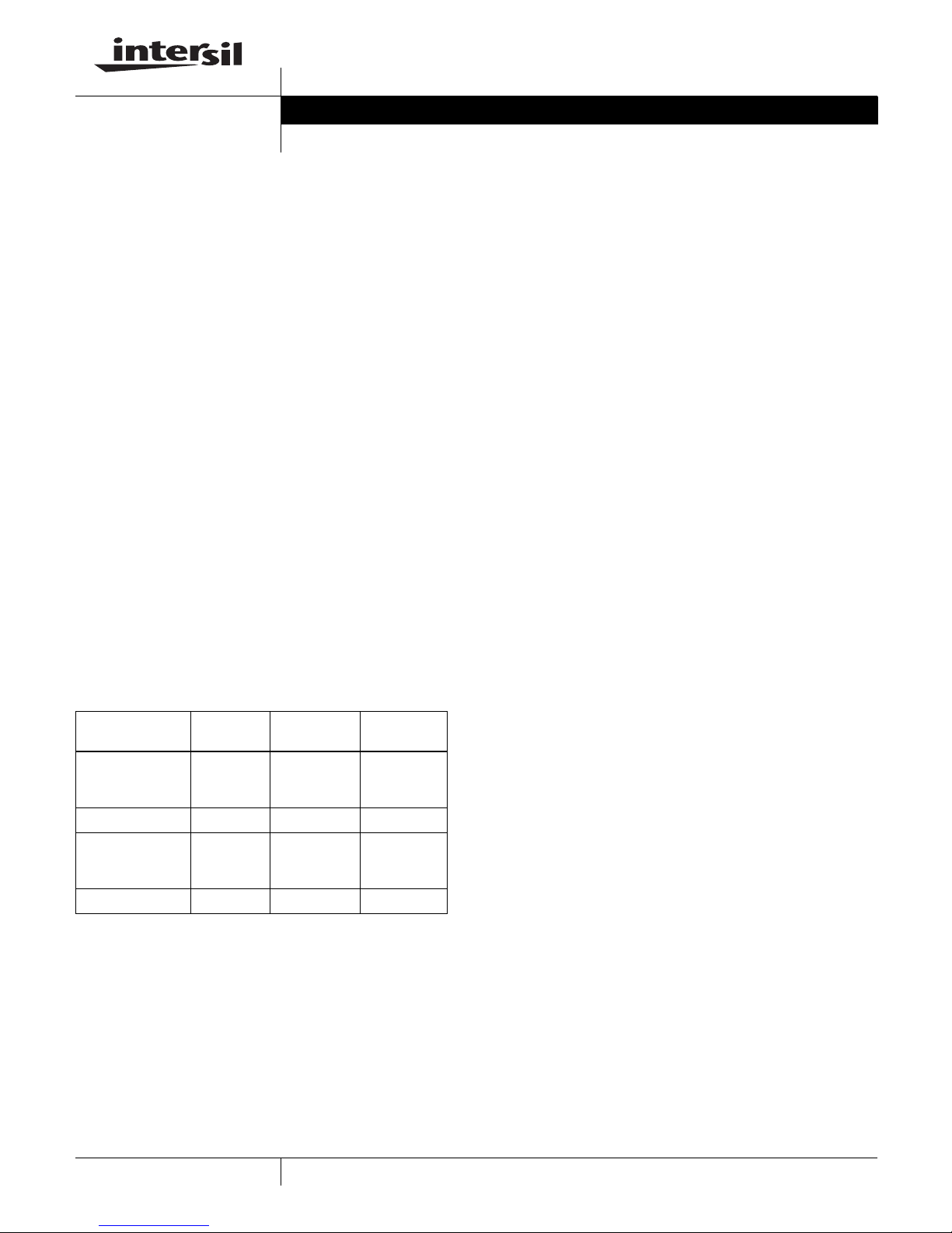
Table 1 - Evaluation Boards
Board Name
Switching
Frequency IC Package
ISL6526EVAL1 300kHz
and
600kHz
ISL6526CB
ISL6526ACB
14 ld SOIC
ISL6526EVAL2 300kHz ISL6526CR 16 ld MLFP
ISL6527EVAL1 300kHz
and
600kHz
ISL6527CB
ISL6527ACB
14 ld SOIC
ISL6527EVAL2 600kHz ISL6527ACR 16 ld MLFP
June 2002
Application Note
Page 2
2
To observe the output while the regulator sinks current,
connect the positive terminal of the load to the 3.3V post
(J1). Connect the return terminal of the same load to the
V
OUT
post (J3).
Startup
There are two distinct start up methods for both the ISL6526
and ISL6527 regulators. The first method is invoked through
the application of power to the IC. The soft-start feature
allows for a controlled rise of the output once the Power On
Reset (POR) threshold of the input voltage has been
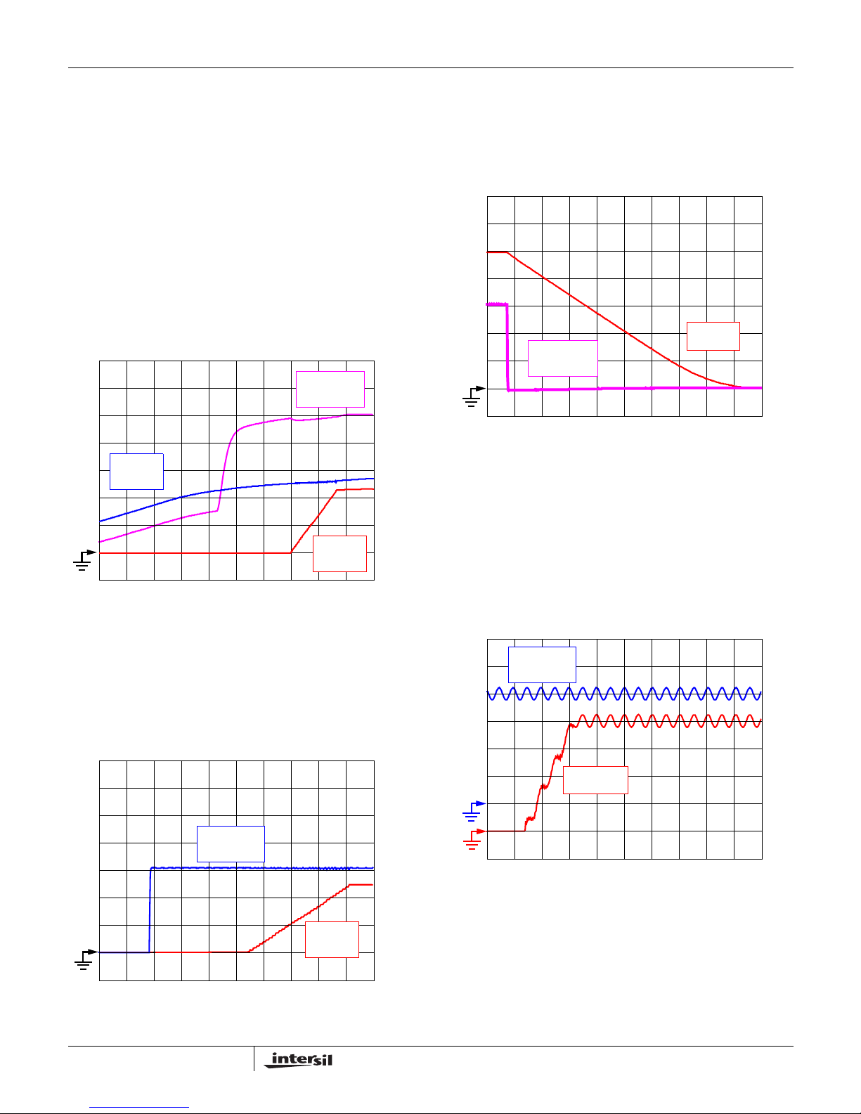
reached. Figure 1 shows the start up profile of the regulator
in relation to the start up of the 3.3V input supply and the
bias supply generated by the charge pump. Both the
ISL6526 and ISL6527, whether switching at 300 or 600kHz,
will have the same start up profile as shown in Figure 1.
The second method of start up is through the use of the
Enable/Shutdown feature. Holding the ENABLE pin on the
ISL6526 or the OCSET/SD pin on the ISL6527 below 0.8V
will disable the regulator by forcing both the upper and lower
MOSFETs off. Releasing the respective pin allows the
regulator to start up. Figure 2 shows the start up profile with
this method.
Shutdown
As discussed in the previous section, if the OCSET/SD pin
or ENABLE pin is pulled down and held below 0.8V, the
regulator will be turned off. The MOSFET gates are
immediately pulled low. Figure 3 shows the shutdown profile
of the regulator under full load.
ISL6527 Input Reference
A distinguishing feature of the ISL6527 is that the reference
used to regulate the output is provided from an external
source. This allows the converter to track the output of
another regulator at any desired ratio or amplify a small
signal. Figure 4 illustrates the tracking and power
amplification ability of the ISL6527 with a sinusoidal
reference. Figure 4 also illustrates the startup profile.
Ripple Voltage
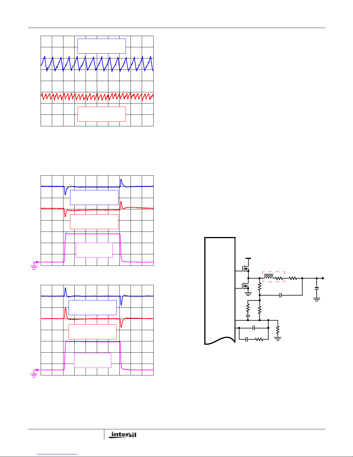
Figure 5 shows the ripple voltage on the output of the
regulator. The ripple voltages shown are for both the
ISL6526 and ISL6527 ICs running at either 300 or 600kHz.
FIGURE 1. START UP FROM POR
2ms/DIV
V
CPVOUT
1V/DIV
V
VCC
1V/DIV
V
OUT
1V/DIV
FIGURE 2. START UP FROM SHUT DOWN
1ms/DIV
V
OUT
1V/DIV
V
ENABLE
1V/DIV
FIGURE 3. SHUTDOWN WITH FULL LOAD (ISL6526)
20µs/DIV
V
ENABLE
1V/DIV
V
OUT
1V/DIV
FIGURE 4. SMALL SIGNAL POWER AMPLIFICATION
2ms/DIV
V
REF_IN
200mV/DIV
V
OUT
200mV/DIV
AN1021
Page 3
3
Transient Performance
Figures 6 and 7 show the response of the output when
subjected to sourcing and sinking transient loading,
respectively.
Lossless Output Voltage Droop
Droop is an intentional sag in the output voltage that is
proportional to the output current. Although not necessary
for proper circuit operation, utilizing droop allows the
dynamic regulation to be improved by taking advantage of
static regulation requirements and expanding the available
headroom for transient edge output excursions. In practical
applications that are compared to a non-droop
implementation, the droop implementation requires fewer
output capacitors or better regulation with the same type and
number of output capacitors.
By moving the regulation point ahead of the output inductor
(at the PHASE node), droop becomes equal to the average
voltage drop across the output inductor’s DC resistance as
well as any distributed resistance. The droop circuitry is
simply an RC low pass filter placed across the output
inductor. This filter must have the same time constant that
the output inductor and it’s corresponding DCR have. The
design must be careful to include any parasitic impedances
of the PC board if the DCR of the inductor is very low.
The ISL6526/27 evaluation board does not have any
component footprints that would allow an implementation of
droop. This section is included in this application note as a
guideline in the event that droop is necessary in a design
utilizing the ISL6526 or ISL6527. Figure 8 shows a
schematic of the power stage and Type III compensation
network of an ISL6526/27 regulator with droop. The droop
circuitry is represented by resistor R
D
and capacitor CD. The
output of this low pass filter is fed directly into the feedback
compensation network of the regulator. To insure symmetric
output voltage excursions about the nominal voltage in
response to load transients, the output voltage should be
programmed to be above the nominal level by half the
calculated droop.
FIGURE 5. OUTPUT RIPPLE VOLTAGE
5µs/DIV
V
OUT
at 300kHz
10mV/DIV
V
OUT
at 600kHz
10mV/DIV
FIGURE 6. SOURCING TRANSIENT
200µs/DIV
Load Current
2A/DIV
V
OUT
at 300kHz
10mV/DIV
V
OUT
at 600kHz
10mV/DIV
FIGURE 7. SINKING TRANSIENT
200µs/DIV
Load Current
2A/DIV
V
OUT
at 300kHz
10mV/DIV
V
OUT
at 600kHz
10mV/DIV
FIGURE 8. DROOP IMPLEMENTATION
+
R
FB
C
OUT
V
OUT
L
OUT
ISL6526
Q
U
FB
UGATE
COMP
LGATE
Q
L
VIN
OR
ISL6527
R
D
C
D
R
OS
DCR
R
parasitic
AN1021
Page 4
4
A properly designed droop implementation will have the time
constant of the RC filter equal to or very close to the time
constant of the output inductor.
Note that the impedance portion of the time constant
calculation for the RC filter includes the parallel combination
of the filter resistor, R
D
, and the feedback resistor, RFB.
Since the regulation point is now located at the phase node,
and a resistor, R
D
, is being added to the DC path for
regulation, then the offset resistor, R
OS
, must be adjusted.
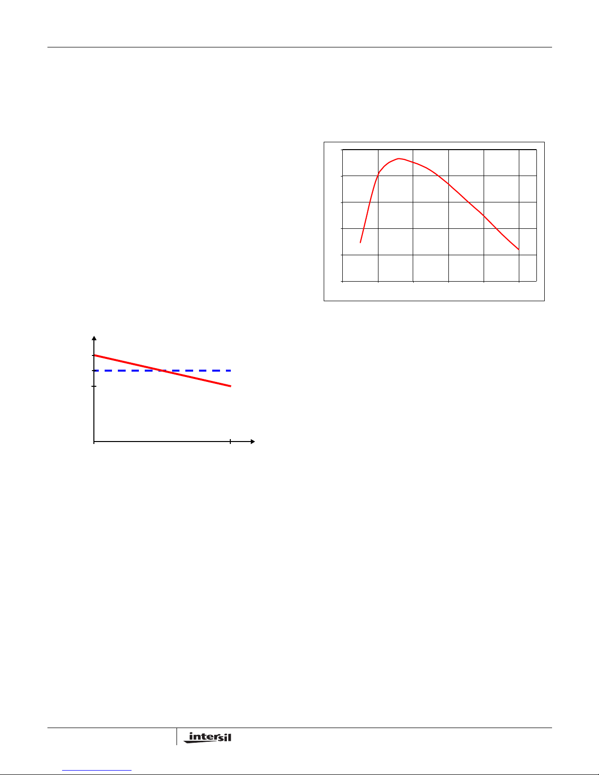
Figure 9 shows the output voltage of the converter with the
droop circuitry added.
With the proper selection of the components used in the RC
filter across the inductor, the frequency response of the
system is only minimally affected and the compensation
network does not need to be recalculated.
Efficiency
The ISL6526 and ISL6527 regulators allow for highly
efficient systems. The efficiency of the evaluation board in is
shown in Figure 10. The efficiencies of the converter for both
sinking and sourcing current are identical.
Conclusion
The ISL6526 and ISL6527 are versatile PWM controllers.
Compact and highly efficient regulators can be implemented
with either IC. Both ICs offer small footprints and features
which make them an ideal for many low voltage power
solutions.
References
For Intersil documents available on the web, see
http://www.intersil.com/
[1] ISL6526 Data Sheet, Intersil Corporation, File No.
FN9055
[2] ISL6527 Data Sheet, Intersil Corporation, File No.
FN9056
τ
out
L
DCR R
parasitic
+
-----------------------------------------------
R
DRFB
||
()C
D
⋅==
R
OS
V
REF
V
NOMINAL
1
2
-- -
I
Omax()
DCR⋅⋅V
REF
–+
----------------------------------------------------------------------------------------------------------
R
FBRD
+()⋅=
Where: V
REF
= 0.8V for ISL6526
V
REF
= External Reference for ISL6527
V
MAX
V
MIN
0A
I
O(max)
WITHOUT DROOP
WITH DROOP
OUTPUT CURRENT
OUTPUT
VO LTAGE
FIGURE 9. OUTPUT VOLTAGE DROOP
V
NOMINAL
FIGURE 10. EFFICIENCY - SINKING AND SOURCING
CURRENT
90
91
92
93
94
95
012345
Load Current (A)
Efficiency (%)
AN1021
Page 5
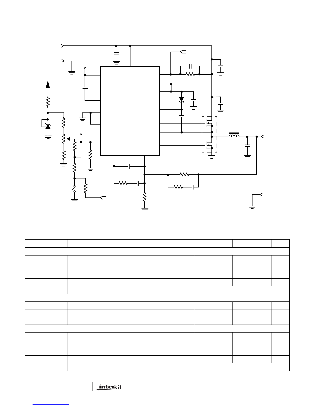
5
Evaluation Board Schematic
NOTE: All evaluation boards share the same schematic.
2.5V @ 5A
FBCOMP
UGATE
PHASE
BOOT
GND
LGATE
ISL6526
R
3
R
5
C
10
C
11
R
2
L
1
D
1
C
7
C
1
C
4
C
6
C
8,9
OCSET(/SD)
CPVOUT
C
3
R
1
Q
1
CT1
CT2
CPGND
ENABLE(EA+)
VCC
3.3V
C
5
PB
1
C
2
C
12
R
4
GND
(ISL6527)
U
1
3.3V
R
7
R
POT1
R
8
GND
14(14)
1(15)
2(16)
3(1)
4(2)
5(3)
8(7)
6(4)
9(8)
10(10)
11(11)
12(12)
13(13)
R
9
R
6
U
2
J
1
J
2
J
3
J
4
TP
1
TP
2
TP
3
6527_SD
6527_SD
R
6527B
R
6526
R
6527A
7(6)
Pin numbers are designated as follows: The first number is the SOIC pin number.
The proceeding number in parentheses is the MLFP pin number.
Table 2 - Evaluation Board Specific Bill of Material
Ref Des Description Vendor Vendor P/N QTY
ISL6526EVAL1 Evaluation Board
U1 ISL6526 300kHz Synchronous Buck PWM Controller - SOIC Intersil ISL6526CB 1
R6526 Zero Ohm Jumper Various --- 1
R6527A,R6527B Unpopulated Zero Ohm Jumper Various --- 0
--- ISL6526A 600kHz Synchronous Buck PWM Controller - SOIC Intersil ISL6526ACB 1
The additional IC is bagged and tagged and shipped with the assembled evaluation board
ISL6526EVAL2 Evaluation Board
U1 ISL6526 300kHz Synchronous Buck PWM Controller - MLFP Intersil ISL6526CR 1
R6526 Zero Ohm Jumper Various --- 1
R6527A,R6527B Unpopulated Zero Ohm Jumper Various --- 0
ISL6527EVAL1 Evaluation Board
U1 ISL6527 300kHz Synchronous Buck PWM Controller - SOIC Intersil ISL6527CB 1
R6526 Unpopulated Zero Ohm Jumper Various --- 0
R6527A,R6527B Unpopulated Zero Ohm Jumper Various --- 2
--- ISL6527A 600kHz Synchronous Buck PWM Controller - SOIC Intersil ISL6527ACB 1
The additional IC is bagged and tagged and shipped with the assembled evaluation board
AN1021
Page 6
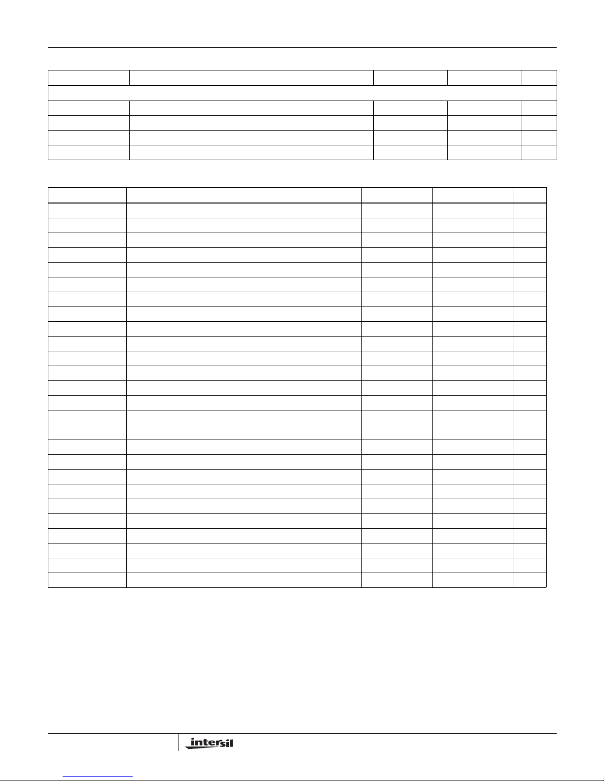
6
ISL6527EVAL2 Evaluation Board
U1 ISL6527A 600kHz Synchronous Buck PWM Controller - MLFP Intersil ISL6527ACR 1
R6526 Unpopulated Zero Ohm Jumper Various --- 0
R6527A,R6527B Zero Ohm Jumper Various --- 2
Table 2 - Evaluation Board Specific Bill of Material (Continued)
Ref Des Description Vendor Vendor P/N QTY
Table 3 - Evaluation Board Common Bill of Material
Ref Des Description Vendor Vendor P/N QTY
C1,C7 0.1µF Capacitor, 0603 Various --- 2
C2 1000pF Capacitor, 0603 Various --- 1
C3,C8,C9 150µF Capacitor Panasonic EEF-UE0J151R 3
C4 0.22µF Capacitor, 0805 Various --- 1
C5 10µF Capacitor Various --- 1
C6 1µF Capacitor, 0805 Various --- 1
C10 33pF Capacitor, 060 3 Various --- 1
C11 5600pF Capacitor, 0603 Various --- 1
C12 8200pF Capacitor, 0603 Various --- 1
D1 Diode, 30mA, 30V Digikey MA732 1
L1 1µH Inductor Panasonic ETQP6F1R0SFA 1
Q1 Dual MOSFET, 8 Pin SOIC Fairchild ITF86110DK8 1
R1 9.76kΩ 1% Resistor, 0603 Various --- 1
R2 6.49kΩ 1% Resistor, 0603 Various --- 1
R3 2.26kΩ 1% Resistor, 0603 Various --- 1
R4 124Ω 1% Resistor, 0603 Various --- 1
R5 1.07kΩ 1% Resistor, 0603 Various --- 1
R6 1.33kΩ 1% Resistor, 0603 Various --- 1
R7 61.9kΩ 1% Resistor, 0603 Various --- 1
R8 13.3kΩ 1% Resistor, 0603 Various --- 1
R9 100kΩ 1% Resistor, 0603 Various --- 1
RPOT1 25 Turn Potentiometer 0Ω to 50kΩ Digikey 3299Y-503-ND 1
PB1 Pushbutton, miniature Digikey P8007S-ND 1
U2 Adjustable Precision Zener Shunt Regulator National LM431CCM3/N1B 1
TP1,TP2,TP3 Test Points Digikey 5002K-ND 3
J1,2,3,4 Test Points Keystone 1514-2 4
AN1021
Page 7
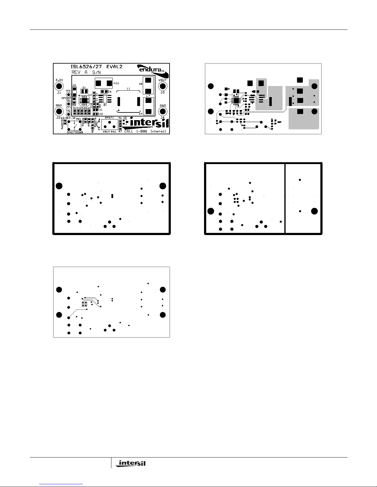
7
Board Description - MLFP
Silk Screen Top Layer
Ground Layer Power Layer
Bottom Layer
AN1021
Page 8
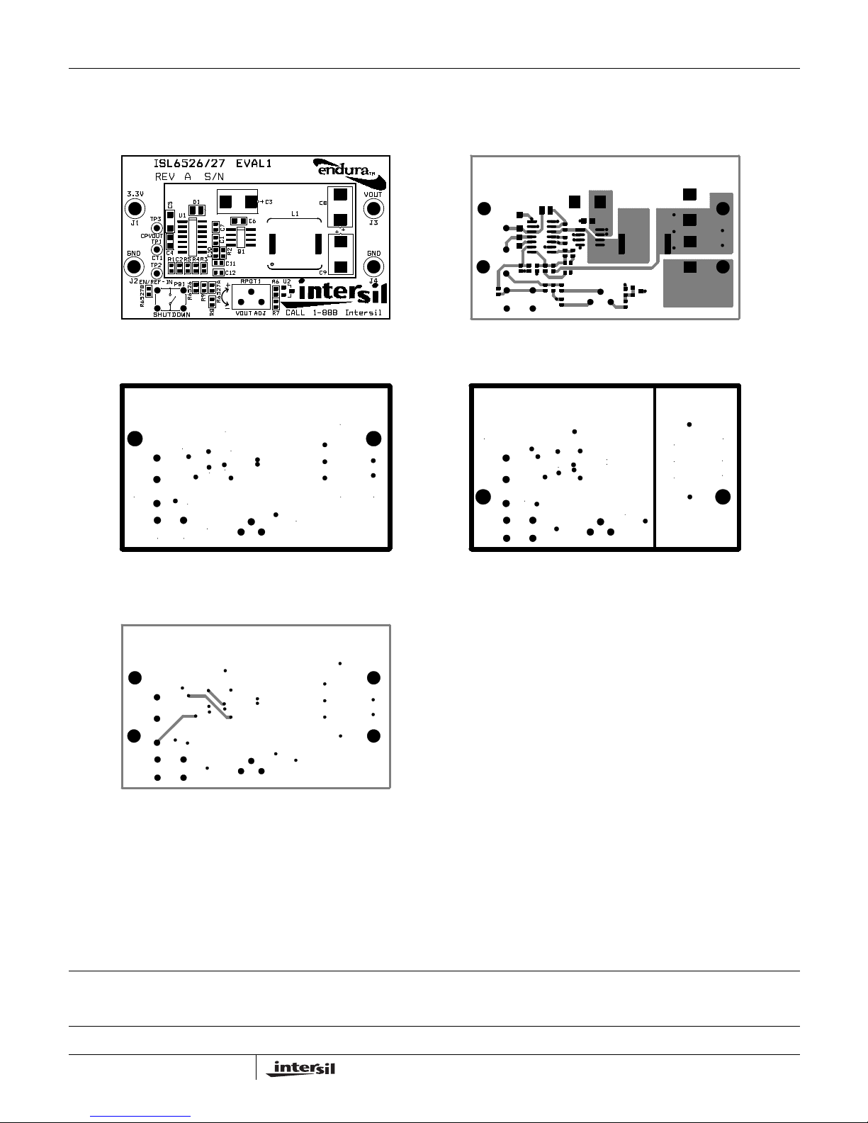
8
All Intersil U.S. products are manufactured, assembled and tested utilizing ISO9000 quality systems.
Intersil Corporation’s quality certifications can be viewed at www.intersil.com/design/quality
Intersil products are sold by description only. Intersil Corporation reserves the right to make changes in circuit design, software and/or specifications at any time without
notice. Accordingly, the reader is cautioned to verify that data she ets are current before placin g orders. Information furn ished by Intersil is believed to be accurate and
reliable. However, no responsibility is assumed by Intersil or its subsidiaries for its use; nor for any infringements of patents or other rights of third parties which may result
from its use. No license is granted by implication or othe rwise under any patent or patent rights of Intersil or its subsidiaries.
For information regarding Intersil Corporation and its products, see www.intersil.com
Board Description - SOIC
Silk Screen Top Layer
Ground Layer Power Layer
Bottom Layer
AN1021
 Loading...