

Page 1
®
www.BDTIC.com/Intersil
ISL6505
Data Sheet December 1, 2005
Multiple Linear Power Controller with
ACPI Control Interface
The ISL6505 complements other power building blocks
(voltage regulators) in ACPI-compliant designs for
microprocessor and computer applications. The IC
integrates three linear controllers/regulators, switching,
monitoring and control functions into a 20-pin wide-body
SOIC or 20-pin QFN (also known as MLF) 5x5 package.
The ISL6505’s operating mode (active or sleep outputs) is
selectable through two digital control pins, S3
One linear controller generates the 3.3V
voltage plane from the ATX supply’s 5V
the south bridge and the PCI slots through an external NPN
pass transistor during sleep states (S3, S4/S5). In active
state (during S0 and S1/S2), the 3.3V
DUAL
regulator uses an external N-channel pass MOSFET to
connect the outputs directly to the 3.3V input supplied by an
ATX power supply, f or minimal losses. Th e 3 .3 V
output is active for as long as the ATX 5V
to the chip.
A controller powers up the 5V
plane by switching in the
DUAL
ATX 5V output through an NMOS transistor in active states,
or by switching in the ATX 5V
through a PMOS (or PNP)
SB
transistor in S3 sleep state. In S4/S5 sleep states, the
ISL6505 5V
output is either shut down or stays on,
DUAL
based on the state of the EN5 pin.
An internal linear regulator supplies the 1.2V for the voltage
identification circuitry (VID) only during active states (S0 and
S1/S2), and uses the 3V3 pin as input source for its internal
pass element.
A linear controller generates V
3.3V
/3.3VSB voltage plane, using an external NFET.
DUAL
OUT1
from the
The voltage is user-programmable to values between 1.2V
and 1.5V, using an external resistor divider. The mode is
user-selectable with the LAN pin; a logic high (or open)
selects the 10/100 LAN mode, wh er e V
(S0-S5); a logic low selects the Gigabit Ethernet mode,
where V
is only on during active modes (S0-S2).
OUT1
and S5.
/3.3VSB
DUAL
output, powering
SB
/3.3VSB linear
/3.3VSB
DUAL
voltage is applied
SB
is always on
OUT1
FN9109.3
Features
• Provides four ACPI-Controlled Voltages
-5V
-3.3V
-1.2V
-V
USB/Keyboard/Mouse
DUAL
/3.3VSB PCI/Auxiliary/LAN
DUAL
Processor VID Circuitry
VID
(1.2V - 1.5V programmable) LAN/Ethernet
OUT1
• Excellent Output Voltage Regulation
- All Outputs: ±2.0% over temperature (as applicable)
• Small Size; Very Low External Component Count
• Undervoltage Monitoring of All Outputs with Centralized
FAULT Reporting and Temperature Shutdown
• QFN Package:
- Compliant to JEDEC PUB95 MO-220
QFN - Quad Flat No Leads - Package Outline
- Near Chip Scale Package footprint, which improves
PCB efficiency and has a thinner profile
• Pb-Free Plus Anneal Available (RoHS Compliant)
Applications
•
ACPI-Compliant Power Regulation for Motherboards
Ordering Information
PART NUMBER
ISL6505CB* 0 to 70 20 Ld Wide SOIC M20.3
ISL6505CR* 0 to 70 20 Ld 5x5 QFN L20.5x5
ISL6505CRZ*
(Note 1)
ISL6505EVAL1 Evaluation Board (SOIC)
ISL6505EVAL2 Evaluation Board (QFN)
Add “-T” suffix for tape and reel.
NOTE:
1. Intersil Pb-free plus anneal products employ special Pb-free
material sets; molding compounds/die attach materials and
100% matte tin plate termination finish, which are RoHS
compliant and compatible with both SnPb and Pb-free soldering
operations. Intersil Pb-free products are MSL classified at
Pb-free peak reflow temperatures that meet or exceed the
Pb-free requirements of IPC/JEDEC J STD-020.
TEMP.
RANGE (°C) PACKAGE
0 to 70 20 Ld 5x5 QFN
(Pb-free)
PKG.
DWG. #
L20.5x5
Pinouts - See page 6.
1
CAUTION: These devices are sensitive to electrostatic discharge; follow proper IC Handling Procedures.
1-888-INTERSIL or 1-888-468-3774
| Intersil (and design) is a registered trademark of Intersil Americas Inc.
All other trademarks mentioned are the property of their respective owners.
Copyright © Intersil Americas Inc. 2004, 2005. All Rights Reserved
Page 2
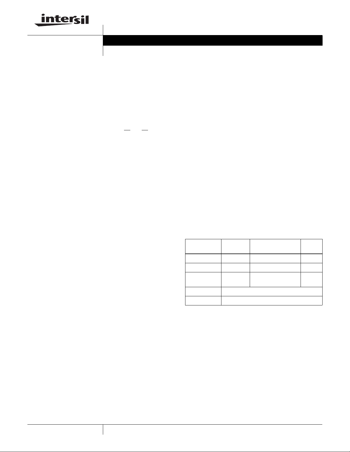
Block Diagram
www.BDTIC.com/Intersil
3V3DLSB
EA4
3V3
3V3DL
+
5V
5VSB
5VSB POR
DLA
5VDLSB
2
5V MONITOR
4.5V/4.25V
EA3
DR1
FB1
+
TO UV
DETECTOR
4.4V/3.4V
3V3 MONITOR
2.75V/2.60V
TEMPERATURE
MONITOR
(TMON)
ISL6505
MONITOR AND CONTROL
TO 3V3
EA3
+
FAULT
UV DETECTOR
UV COMP
4.10V
TO
UV DETECTOR
10µA
+
-
+
-
+
0.80V
-
-
1V2VID
+
-
10mA
VID_PG
5VDL
GND
SS
S3
S5
EN5
FIGURE 1.
LAN
VID_CT
Page 3
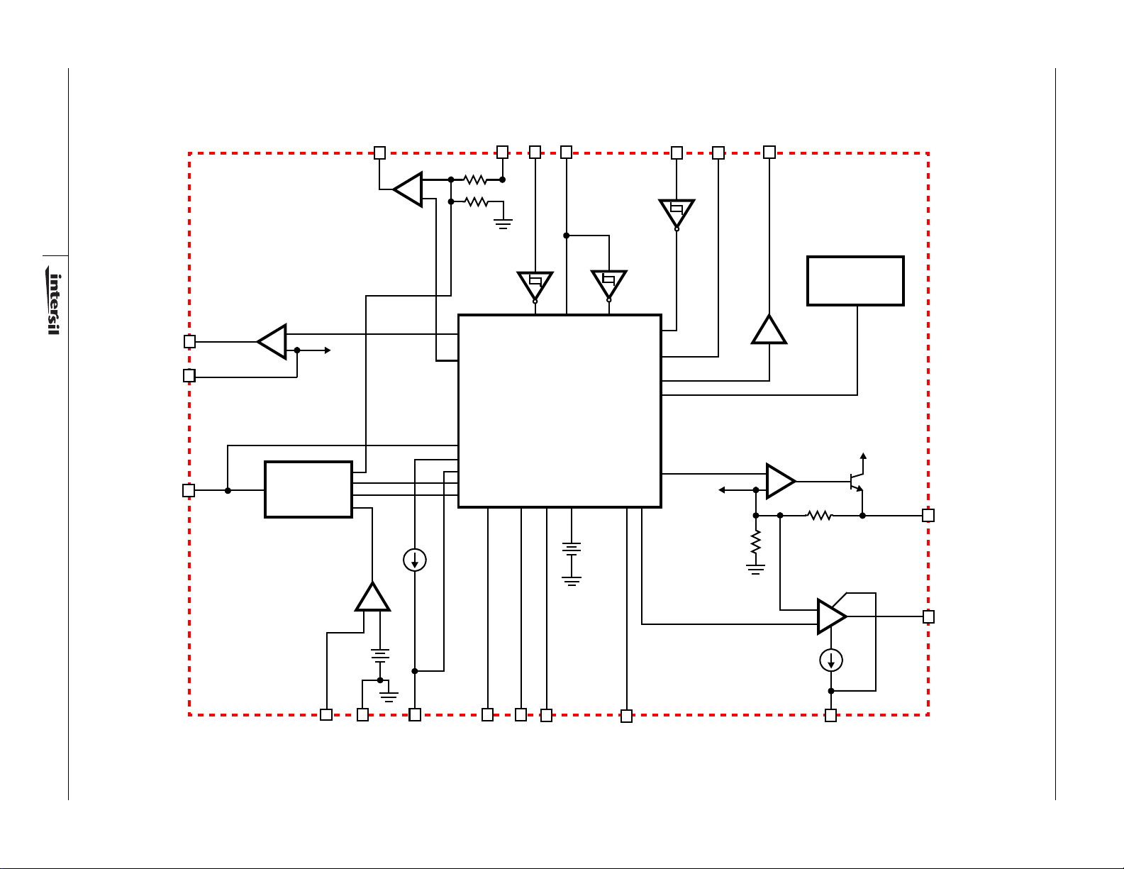
Simplified Power System Diagram
www.BDTIC.com/Intersil
+5V
IN
+12V
IN
+5V
SB
+3.3V
IN
ISL6505
FAULT
Q2
3.3V
SHUTDOWN
SX, EN5, LAN
DUAL
V
/3.3V
OUT1
SB
3.3V
4
Typical Application
+5V
IN
+12V
IN
+5V
SB
+3.3V
IN
V
OUT1
1.2V - 1.5V
Q2
C
OUT1
Q3
R21
Q6
R20
R
DLA
Q6
R20
R21
3V3DLSB
ISL6505
LINEAR
CONTROLLER
LINEAR
CONTROLLER
FIGURE 2.
DR1
FB1
3V3
REGULATOR
5V
LINEAR
CONTROL
LOGIC
5VSB
1V2VID
VID_CT
C
CT_VID
1.2V
VID
1.2V
VID_PG
C
OUT2
Q5
Q4
V
OUT2
1.2V
5V
DUAL
5V
VID
VID_PG
5VDLSB
DLA
5VDL
3.3V
FAULT
SLP_S3
SLP_S5
SHUTDOWN
V
DUAL
OUT3
/3.3V
SB
C
OUT3
Q3
EN5
LAN
3V3DL
EN5
LAN
FAULT
C
SS
ISL6505
S3
S5
SS
GND
FIGURE 3.
3
C
OUT4
Q5
VID PGOOD
Q4
V
5V
OUT4
DUAL
Page 4
ISL6505
www.BDTIC.com/Intersil
Absolute Maximum Ratings Thermal Information
Supply Voltage, V
DLA . . . . . . . . . . . . . . . . . . . . . . . . . . . . . . . . GND - 0.3V to +14.5V
All Other Pins. . . . . . . . . . . . . . . . . . . . . . . . . . . . . . . . . . . . . .+ 7.0V
ESD Classification (Human Body Model) . . . . . . . . . . . . . . . . . .2kV
Recommended Operating Conditions
Supply Voltage, V
Lowest 5VSB Supply Voltage Guaranteeing Parameters . . . . +4.5V
Digital Inputs, V
Ambient Temperature Range. . . . . . . . . . . . . . . . . . . . . 0
Junction Temperature Range. . . . . . . . . . . . . . . . . . . . 0
CAUTION: Stresses above those listed in “Absolute Maximum Ratings” may cause permanent damage to the device. This is a stress only rating and operation of the
device at these or any other conditions above those indicated in the operational sections of this specification is not implied.
NOTES:
2. θ
is measured with the component mounted on a high effective thermal conductivity test board in free air. See Tech Brief TB379 for details.
JA
is measured in free air with the component mounted on a high effective thermal conductivity test board with “direct attach” features. See
3. θ
JA
Tech Brief TB379.
4. For θ
, the “case temp” location is the center of the exposed metal pad on the package underside.
JC
Electrical Specifications Recommended Operating Conditions, Unless Otherwise Noted Refer to Figures 1, 2 and 3
VCC SUPPLY CURRENT
Nominal Supply Current I
Shutdown Supply Current I
POWER-ON RESET, SOFT-START, AND VOLTAGE MONITORS
5VSB Rising POR Threshold 4.0 4.3 4.5 V
5VSB Falling POR Threshold 3.15 3.4 3.55 V
5VSB POR Hysteresis -0.9- V
3V3 Rising Threshold 2.8 2.93 3.0 V
3V3 Falling Threshold 2.65 2.78 2.9 V
3V3 Hysteresis - 150 - mV
5V Rising Threshold 4.25 4.4 4.5 V
5V Falling Threshold 4.0 4.15 4.3 V
5V Hysteresis - 250 - mV
VID_PG Rising Threshold -1.04- V
VID_PG Hysteresis -50- mV
VID_CT Charging Current I
Soft-Start Current I
Soft-Start Shutdown Voltage Threshold V
LINEAR REGULATOR (V
Regulation V
V
OUT1
Nominal Voltage Level V
V
OUT1
Undervoltage Rising Threshold FB1 pin - 1.2 - V
V
OUT1
Undervoltage Hysteresis FB1 pin - 50 - mV
V
OUT1
DR1 Output Drive Current I
. . . . . . . . . . . . . . . . . . . . . . . . . . . . . . +7.0V
5VSB
. . . . . . . . . . . . . . . . . . . . . . . . . . . +5V ±5%
5VSB
. . . . . . . . . . . . . . . . . . . . . . . . . . . . . . .0 to +5.5V
Sx
PARAMETER SYMBOL TEST CONDITIONS MIN TYP MAX UNITS
; DR1 and FB1 pins)
OUT1
o
C to 70oC
o
C to 125oC
5VSB
5VSB(OFF)VSS
VID_CT
SS
SD
OUT1
DR1
V
VID_CT
OUT1
Based on external resistors - 1.5 - V
V
3V3DL
= 0.8V - 4 - mA
= 1.2V to 1.5V - - 2.0 %
= 3.3V - 10 - mA
Thermal Resistance (Typical)
SOIC Package (Note 2). . . . . . . . . . . . 65 N/A
QFN Package (Notes 3, 4) . . . . . . . . . 35 5
Maximum Junction Temperature (Plastic Package) . . . . . . . .150
Maximum Storage Temperature Range. . . . . . . . . . -65
Maximum Lead Temperature (Soldering 10s) . . . . . . . . . . . . .300
(SOIC - Lead Tips Only)
= 0V - 10 - µA
θ
(oC/W) θJC (oC/W)
JA
o
C to 150oC
-6- mA
-10- µA
--0.8V
o
C
o
C
4
Page 5
ISL6505
www.BDTIC.com/Intersil
Electrical Specifications Recommended Operating Conditions, Unless Otherwise Noted Refer to Figures 1, 2 and 3 (Continued)
PARAMETER SYMBOL TEST CONDITIONS MIN TYP MAX UNITS
1.2V
LINEAR REGULATOR (V
VID
1V2VID Regulation --2.0%
1V2VID Nominal Voltage Level V
1V2VID Undervoltage Rising Threshold -0.92- V
1V2VID Undervoltage Hysteresis - 100 - mV
1V2VID Output Current I
3.3V
3V3DL Sleep State Regulation --2.0%
3V3DL Nominal Voltage Level V
3V3DL Undervoltage Rising Threshold -2.62- V
3V3DL Undervoltage Hysteresis - 150 - mV
3V3DLSB Output Drive Current I
5V
5VDL Undervoltage Rising Threshold -4.10- V
5VDL Undervoltage Hysteresis - 120 - mV
5VDLSB Output Drive Current I
TIMING INTERVALS
Active State Assessment Past Input UV
Thresholds (Note 5)
Active-to-Sleep Control Input Delay - 200 - µs
Falling UV Threshold Timeout (All Monitors) - 10 - µs
CONTROL I/O (S3
High Level Input Threshold S3, S5, EN5, LAN - - 2.2 V
Low Level Input Threshold S3
Internal Pull-up Current to 5VSB S3
Internal Pull-up Current to 5VSB EN5, LAN to GND - 10 - µA
Input Leakage Current to 5VSB EN5, LAN to 5VSB - - 10 mA
FAULT Current IOH (to 5VSB) FAULT = 4.6V, 5VSB = 5V - -7.5 - mA
FAULT Current IOL (to GND) FAULT = 0.4V, 5VSB = 5V - 0.75 - mA
TEMPERATURE MONITOR
Fault-Level Threshold (Note 6) 125 - Shutdown-Level Threshold (Note 6) - 155 -
NOTES:
5. Guaranteed by Correlation.
6. Guaranteed by Design.
/3.3VSB LINEAR REGULATOR (V
DUAL
SWITCH CONTROLLER (V
DUAL
, S5, EN5, LAN, FAULT)
OUT2
OUT4
)
OUT3
3V3DLSBV5VSB
)
1V2VID
V
1V2VID
)
3V3DL
5VDLSBV5VDLSB
= 3.3V - - 180 mA
3V3
= 5V 30 50 - mA
, S5, EN5, LAN 0.8 - - V
, S5 to GND - 50 - µA
= 4V, V
-1.2- V
-3.3- V
= 5V -20 - -40 mA
5VSB
42 53 64 ms
o
C
o
C
5
Page 6
Pinouts
www.BDTIC.com/Intersil
ISL6505 (20 LEAD WIDE SOIC)
TOP VIEW
ISL6505
ISL6505 (5X5 QFN)
TOP VIEW
FB1
DR1
3V3DLSB
3V3DL
1V2VID
3V3
5V
EN5
S3
S5
1
2
3
4
5
6
7
8
9
10
20
19
18
17
16
15
14
13
12
11
5VSB
VID_CT
VID_PG
SS
LAN
5VDL
5VDLSB
DLA
FAULT
GND
3V3DL
1V2VID
3V3
5V
EN5
NOTE: The QFN bottom pad is electrically connected to the IC
substrate, at GND potential. It can be left unconnected, or connected
to GND; do NOT connect to another potential.
Functional Pin Description (Pin numbers for SOIC and QFN)
3V3 (Pin 6 SOIC; Pin 3 QFN)
Connect this pin to the ATX 3.3V output. This pin provides
the output current for the 1V2VID pin, and is monitored for
power quality.
5V (Pin 7 SOIC; Pin 4 QFN)
Connect this pin to the ATX 5V output. This pin is only
monitored for power quality.
5VSB (Pin 20 SOIC; Pin 17 QFN)
Provide a very well de-coupled 5V bias supply for the IC to
this pin by connecting it to the ATX 5V
output. This pin
SB
provides all the chip’s bias as well as the base current for Q2
(see typical application diagram). The voltage at this pin is
monitored for power-on reset (POR) purposes.
GND (Pin 11 SOIC; Pin 8 QFN)
Signal ground for the IC. All voltage le vels are measured with
respect to this pin.
S3 and S5 (Pins 9, 10 SOIC; Pins 6, 7 QFN)
These pins switch the IC’s operating state from active (S0,
S1/S2) to S3 and S4/S5 sleep states. These are digital
inputs featuring internal 50µA (typical) current source pullups to 5VSB. Internal circuitry de-glitches these pins for
disturbances lasting as long as 2µs (typically). Additional
circuitry blocks illegal state transitions (such as S4/S5 to S3),
but does allow S3 to S4/S5. Connect S3
respectively to the computer system’s SLP_S3
signals.
and S5
and SLP_S5
EN5 (Pin 8 SOIC; Pin 5 QFN)
This digital input selects whether the 5VDL output stays up
or shuts down during the S5 Sleep Mode. It has a 10µA
typical pull-up current source. A logic high (5V) or open will
keep the 5VDL on during S5; a logic low (GND) will shut it off
during S5. NOTE: This pin should be tied low or high (or
open) on the board; it was not designed to be changed
during normal operation.
LAN (Pin 16 SOIC; Pin 13 QFN)
This digital input selects between two modes for the V
regulator. It has a 10µA pull-up current source. A logic high
(5V) or open selects the 10/100 LAN mode, where V
stays on all of the time (active and sleep modes). A logic low
(GND) selects the Gigabit Ethernet mode, where V
only on during active (S0, S1) modes. Note that this
selection is independent of the voltage selection of V
(which is determined by the external resistor divider). NOTE:
This pin should be tied low or high (or open) on the board; it
was not designed to be changed during normal operation.
FAULT (Pin 12 SOIC; Pin 9 QFN)
This digital output pin is used to report the fault condition by
being pulled to 5VSB (pulled to GND if no fault). It is a
CMOS digital output; an external pull-down resistor is NOT
required. In case of an undervoltage on any of the controlled
outputs, on any of the monitored ATX voltages (3V3 or 5V;
not 12V), or in case of an overtemperature event, t his pi n is
used to report the fault condition.
3V3DLSB
DR1
FB1
20 19 18 17 16
1
2
3
4
5
678910
S3
S5
GND
5VSB
VID_CT
VID_PG
15
14
SS
13
LAN
5VDL
12
5VDLSB
11
DLA
FAULT
OUT1
OUT1
is
OUT1
OUT1
6
Page 7

ISL6505
www.BDTIC.com/Intersil
SS (Pin 17 SOIC; Pin 14 QFN)
Connect this pin to a small ceramic capacitor (no less than
5nF; 0.1µF recommended). The internal soft-start (SS)
current source along with the external capacitor creates a
voltage ramp used to control the ramp-up of the output
voltages. Pulling this pin low (to GND) with an open-drain
device shuts down all the outputs as well as forces the
FAULT pin low. The C
controlled voltage slew rate during active-to-sleep transitions
on the 3.3V
DUAL
capacitor is also used to provide a
SS
/3.3VSB output.
3V3DL (Pin 4 SOIC; Pin 1 QFN)
Connect this pin to the 3.3V dual/stand-by output (V
In sleep states, the voltage at this pin is regulated to 3.3V; in
active states, ATX 3.3V output is delivered to this node
through a fully-on NFET transistor. During all operating
states, this pin is monitored for undervoltage events. This pin
provides all the output current delivered by V
OUT1
.
OUT3
).
3V3DLSB (Pin 3 SOIC; Pin 20 QFN)
Connect this pin to the base of a suitable NPN transistor. In
sleep state, this transistor is used to regulate the voltage at
the 3V3DL pin to 3.3V.
DLA (Pin 13 SOIC; Pin 10 QFN)
This pin is an open-collector output. Connect a 1kΩ resistor
from this pin to the ATX 12V output. This resistor is used to
pull the gates of suitable NFETs to 12V, which in acti ve sta te,
switch in the ATX 3.3V and 5V outputs into the
3.3V
/3.3VSB and 5V
DUAL
outputs, respectively.
DUAL
5VDL (Pin 15 SOIC; Pin 12 QFN)
Connect this pin to the 5V
operating state (when on), the voltage at this pin is provided
through a fully-on MOSFET transistor. This pin is also
monitored for undervoltage events.
DUAL
output (V
OUT4
). In either
5VDLSB (Pin 14 SOIC; Pin 11 QFN)
Connect this pin to the gate of a suitable PFET or bipolar
PNP. This transistor is switched on, connecting the ATX
5V
output to the 5V
SB
if EN5 is open or high, during S5. If EN5 is low (GND), the
transistor is switched off in S5.
regulator output during S3, and
DUAL
DR1 (Pin 2 SOIC; Pin 19 QFN)
This output pin drives the gate of an external NFET
transistor to create V
from the 3V3DL pin.
, which draws its output curr en t
OUT1
FB1 (Pin 1 SOIC; Pin 18 QFN)
This analog input pin looks at the V
divider, and compares it to the internal reference (0.8V
nominal), in order to regulate the voltage on V
is also monitored for undervoltage events.
external resistor
OUT1
OUT1
. This pin
1V2VID (Pin 5 SOIC; Pin 2 QFN)
This pin is the output of the internal 1.2V voltage identification
(VID) regulator (V
). This internal regulator operates only
OUT2
in active states (S0, S1/S2) and is shut off during any sleep
state. This regulator draws its output current from the 3V3 pin.
This pin is monitored for undervoltage e vents.
VID_PG (Pin 18 SOIC; Pin 15 QFN)
This pin is the open collector output of the 1V2VID power
good comparator. Connect a 10kΩ pull-up resistor from this
pin to the 1V2VID output. As long as the 1V2VID output is
below its PG threshold (typically 90% of final value), this pin
is pulled low. Once the PG threshold is reached, the VID_CT
pin starts charging its capacitor (setting the delay); when it
reaches its trip point, then the VID-PG pin releases, and
goes high (through the external pull-up resistor).
VID_CT (Pin 19 SOIC; Pin 16 QFN)
Connect a small capacitor from this pin to ground. The
capacitor is used to delay the VID_PG reporting the 1V2VID
has reached power good limits.
Description
Operation
The ISL6505 controls 4 output voltages (Refer to Figures 1,
2, and 3). It is designed for microprocessor computer
applications with 3.3V, 5V, 5V
ATX power supply. The IC is composed of three linear
controllers/regulators supplying the computer system’s
V
(1.2V - 1.5V programmable), 3.3VSB and PCI slots’
OUT1
3.3V
(V
voltage (V
functions necessary for complete ACPI implementation.
power (V
AUX
), a dual switch controller supplying the 5V
OUT2
), as well as all the control and monitoring
OUT4
), the 1.2V VID circuitry power
OUT3
Initialization and POR
The ISL6505 automatically initializes upon receipt of input
power. The Power-On Reset (POR) function continually
monitors the 5V
3.3V
after exceeding POR threshold.
Note that while the 5VSB pin has the main POR, both the
3V3 and 5V pins (12V is not monitored) must rise above their
own POR levels (typically 90%) in order to transition into the
S0/S1 active state. If during normal operation either one
drops below their falling trip points, the IC will go to the S5
sleep mode. When both are back above their rising
thresholds, the IC will again soft-start into active state.
/3.3VSB and 1.5VSB soft-start operation shortly
DUAL
input supply voltage, initiating
SB
Output Operational Truth Tables
Table 1 describes the tr uth combinations pertaining to the
3.3V
DUAL/SB
highlight the difference between EN5 connected high or low.
Table 2 describes the tr uth combinations pertaining to the
V
OUT1
outputs. The last two sets of lines highlight the difference
between the two LAN pin modes (5V/open is the 10/100 LAN
mode; GND is the Gigabit Ethernet mode).
and 5V
(typically between 1.2V and 1.5V) and 1V2VID
DUAL
, and 12V bias input from an
SB
DUAL
dual outputs. The last two lines
7
Page 8

The internal circuitry does not allow the transition from an
www.BDTIC.com/Intersil
S4/S5 (suspend to disk/soft off) state to an S3 (suspend to
RAM) state; however, i t does allow the transition from S3 to
S4/S5. The only ‘legal’ transitions are from an active state
(S0, S1) to a sleep state (S3, S5) and vice versa.
T ABLE 1. 5V
S5 S3
1 1 3.3V 5V S0/S1/S2 States (Active)
1 0 3.3V 5V S3
0 1 Note Maintains Previous State
0 0 3.3V 0V S4/S5 (EN5 = GND)
0 0 3.3V 5V S4/S5 (EN5 = open/5V)
NOTE: Combination Not Allowed.
TABLE 2. V
S5 S3
1 1 1.5V 1.2V S0/S1/S2 States (Active)
OUTPUT (V
DUAL
TRUTH TABLE
3.3VDL/SB 5VDL COMMENTS
AND 1V2VID (V
OUT1
V
OUT1
) AND 3.3VDL/SB (V
OUT4
) TRUTH TABLE
OUT2
1V2VID COMMENTS
OUT3
ISL6505
)
5VSB
S3
S5
3.3V, 5V
3V3DLSB
DLA
3V3DL
5VDLSB
5VDL
FIGURE 4. 5V
5VSB
AND 3.3V
DUAL
DIAGRAM; EN5 = GND
DUAL
/3.3VSB TIMING
1 0 0V 0V S3 (LAN = GND)
1 0 1.5V 0V S3 (LAN = open/5V)
0 1 Note Maintains Previous State
0 0 0V 0V S4/S5 (LAN = GND)
0 0 1.5V 0V S4/S5 (LAN = open/5V)
NOTE: Combination Not Allowed.
Functional Timing Diagrams
Figures 4 (EN5 = low), 5 (EN5 = high), and 6 are timing
diagrams, detailing the power up/down sequences of all the
outputs in response to the status of the sleep-state pins (S3
S5
), as well as the status of the input ATX supply. Not shown in
these diagrams is the deglitching feature used to protect
against false sleep state tripping. Both S3
and S5 pins are
protected against noise by a 2µs filter (typically 1–4µs). This
feature is useful in noisy computer environments if the control
signals have to trav el over significant distances. Additionally , the
S3
pin features a 200µs delay in transitioning to sleep states.
Once the S3
end of the 200µs interval, if the S5
switches into S5 sleep stat e; if the S5
pin goes low, an internal timer is activated. At the
pin is low, the ISL6505
pin is high, the
ISL6505 goes into S3 sleep state.
The shaded column in Figures 4 and 5 highlights the
difference on the 5VDLSB and 5VDL pins for the two EN5
states.
,
S3
S5
3.3V, 5V
3V3DLSB
DLA
3V3DL
5VDLSB
5VDL
FIGURE 5. 5V
5VSB
S3
S5
3.3V,
5V, 12V
DLA
V
OUT1
(LAN=5V)
1V2VID
(LAN=GND)
V
OUT1
FIGURE 6. V
AND 3.3V
DUAL
DIAGRAM; EN5 = 5V/OPEN
AND 1.2V
OUT1
THE DEPENDENCE OF V
ST ATE OF LAN PIN)
/3.3VSB TIMING
DUAL
TIMING DIAGRAM ( NOTE
VID
OUT1
ON THE LOGIC
8
Page 9

Soft-Start into Sleep States (S3, S4/S5)
www.BDTIC.com/Intersil
The 5VSB POR function initiates the soft-start sequence. An
internal 10µA current source charges an external capacitor.
The error amplifiers’ reference inputs are clamped to a level
proportional to the SS (soft-start) pin voltage. As the SS pin
voltage slews from about 1.4V to 3.0V, the input clamp
allows a rapid and controlled output voltage rise.
ISL6505
5V
SB
(1V/DIV)
SOFT-START
(1V/DIV)
Figures 7 (EN5 = low) and 8 (EN5 = high) show the soft-start
sequence for the typical application start-up into a sleep
state. At time T0 5V
T1, the 5V
surpasses POR level. An internal fast charge
SB
(bias) is applied to the circuit. At time
SB
circuit quickly raises the SS capacitor voltage to
approximately 1V, then the 10µA current source continues
the charging.
5V
SB
(1V/DIV)
SOFT-START
(1V/DIV)
0V
V
(5V
OUT4
V
(3.3V
OUT3
OUTPUT
VOLTAGES
(1V/DIV)
0V
T1 T2
T0
FIGURE 7. SOFT -ST AR T INTERVAL IN A SLEEP STA TE; EN5
= GND; LAN = 5V/OPEN
T3
DUAL
V
OUT1
TIME
/3.3VSB)
T4
V
OUT4
(5V
T5
DUAL
DUAL
) if S5
) if S3
V
OUT2
(1.2V
VID
)
0V
V
(5V
DUAL
V
(1.2V
)
OUT2
VID
)
OUT4
V
(3.3V
OUT3
OUTPUT
VOLTAGES
(1V/DIV)
0V
T1 T2
T0
FIGURE 8. SOFT-START INTERVAL IN A SLEEP STATE;
EN5 = 5V/OPEN; LAN = 5V/OPEN
T3
DUAL
V
OUT1
/3.3VSB)
TIME
T5
T4
The soft-start capacitor voltage reaches approximately 1.4V
at time T2, at which point the 3.3V
/3.3VSB and V
DUAL
OUT1
error amplifiers’ reference inputs start their transition,
resulting in the output voltages ramping up proportionally.
The ramp-up continues until time T3 when the two voltages
reach the set value. As the soft-start capacitor voltage
reaches approximately 3.0V, the undervoltage monitoring
circuit of this output is activated and the soft-start capacitor
is quickly discharged to approximately 1.4V. Following the
3ms (typical) time-out between T3 and T4, the soft-start
capacitor commences a second ramp-up designed to
smoothly bring up the remainder of the voltages required by
the system. At time T5, voltages are within regulation limits,
and as the SS voltage reaches 3.0V, all the remaining UV
monitors are activated and the SS capacitor is quickly
discharged to 1.4V, where it remains until the next transition.
As the 1.2V
output is only on while in an active state, it
VID
does not come up, but rather waits until the main ATX
outputs come up within regulation limits.
Note that in Figures 7 and 8, LAN = 5V/open. If the LAN pin
is connected to GND instead, then the V
not turn on at all in either sleep mode (S3 or S4/S5).
Soft-Start into Active States (S0, S1)
If both S3 and S5 are logic high at the time the 5VSB is
applied, the ISL6505 will assume active state wake-up and
keep off the required outputs until some time (typically 50ms)
after the monitored main ATX outputs (3.3V and 5V; 12V is
not monitored here) exceed the set thresholds. This time-out
feature is necessary in order to ensure the main ATX outputs
are stabilized. The time-out also assures smooth transitions
from sleep into active when sleep states are being
9
output does
OUT1
Page 10

ISL6505
www.BDTIC.com/Intersil
supported. 3.3V
/3.3VSB and V
DUAL
outputs will come
OUT1
up right after bias voltage surpasses POR level (but if LAN =
GND, then V
ramp, along with V
output will not come up until the soft-start
OUT1
; see Figure 9).
OUT2
During sleep-to-active state transitions from conditions
where the 5V
output is initially GND (such as S5 to S0
DUAL
transition, or simple power-up sequence directly into active
state), the circuit goes through a quasi soft-start, the
5V
output being pulled high through the body diode of
DUAL
the NMOS FET connected between it and the 5V ATX.
Figure 9 exemplifies this start-up case. 5V
is already
SB
present when the main ATX outputs are turned on, at time
T0. As a result of +5V
ramping up, the 5V
IN
DUAL
output
capacitors charge up through the body diode of Q5 (see
Typical Application). At time T1, all main A TX outputs e xceed
the ISL6505’s undervoltage thresholds, and the internal
50ms (typical) timer is initiated. At T2, the time-out initiates a
soft-start, and the 1.2V voltage ID output is ramped-up,
reaching regulation limits at time T3. Simultaneous with the
beginning of this ramp-up, at time T2, the DLA pin is
released, allowing the pull-up resistor to turn on Q3 and Q5,
and bring the 5V
output in regulation. Shortly after time
DUAL
T3, as the SS voltage reaches 3.0V, the soft-start capacitor
is quickly discharged down to approximately 2.7V, where it
remains until a valid sleep state request is received from the
system.
+12V
IN
INPUT VOLTAGES
(2V/DIV)
+5V
+5V
SB
0V
OUTPUT
VOLTAGES
(1V/DIV)
0V
T0
FIGURE 9. SOFT-START INTERVAL IN ACTIVE STATE
IN
+3.3V
IN
V
(3.3V
OUT3
V
OUT1
T1 T2
DUAL
(LAN = 5V)
SOFT-START
/3.3VSB)
TIME
DLA PIN
(2V/DIV)
(1V/DIV)
V
OUT4
(5V
V
T3
DUAL
V
OUT2
OUT1
)
(1.2V
(LAN = GND)
VID
)
Fault Protection
All of the outputs are monitored against undervoltage events.
A severe overcurrent caused by a failed load on any of the
outputs, would, in turn, cause that specific output to
suddenly drop. If any of the output voltages drops below 80%
(typical) of their set value, such event is reported by having
the FAULT pin pulled to 5V. Additionally, exceeding the
maximum current rating of an integrated regulator (output
with pass transistor on-chip) can lead to output voltage
drooping; if excessive, this droop can ultimately trip the
undervoltage detector and send a FAULT signal to the
computer system.
A FAULT condition occurring on an output when controlled
through an external pass transistor will only set off the
FAULT flag, and it will not shut off or latch off any part of the
circuit. A F AULT condition occurring on an output controlled
through an internal pass transistor (1V2VID only), will set off
the FAULT flag, and it will shut off the respective faulting
regulator (1V2VID only). If shutdown or latch off of the entire
circuit is desired in case of a fault, regardless of the cause,
this can be achieved by externally pulling or latching the SS
pin low. Pulling the SS pin low will also force the FAULT pin
to go low and reset any internally latched-off output.
Special consideration is given to the initial start-up
sequence. If, following a 5V
or 3.3V
/3.3VSB outputs is ramped up and is subject to
DUAL
an undervoltage event before the end of the second softstart ramp, then the FAULT output goes high and the entire
IC latches off. Latch-off condition can be reset by cycling the
bias power (5V
the 3.3V
DUAL
). Undervoltage events on the V
SB
/3.3VSB outputs at any other times are
handled according to the description found in the second
paragraph under the current heading.
Another condition that could set off the FAULT flag is chip
overtemperature. If the ISL6505 reaches an internal
temperature of 140
o
C (typical), the FAULT flag is set, but the
chip continues to operate until the temperature reaches
o
155
C (typical), when unconditional shutdown of all outputs
takes place. Operation resumes only after powering down
the IC (to create a 5V
SB
(assuming the cause of the fault has been removed; if not, as
it heats up again, it will repeat the FAULT cycle).
In ISL6505 applications, loss of the active ATX output (3V3
or 5V, as detected by the on-board voltage monitor) during
active state operation causes the chip to switch to S5 sleep
state, in addition to reporting the input UV condition on the
F AULT pin. Exiting from this forced S5 state can only be
achieved by returning the faulting input voltage above its UV
threshold, by resetting the chip through remo val of 5V
bias voltage, or by bringing the SS pin at a potential lower
than 0.8V.
POR event, any of the V
SB
OUT1
POR event) and a start-up
OUT1
and
SB
10
Page 11
ISL6505
www.BDTIC.com/Intersil
Application Guidelines
Soft-Start Interval
The 5VSB output of a typical ATX supply is capable of
725mA, with newer models rated for 1.0A, and even 2.0A.
During power-up in a sleep state, the 5V
needs to provide sufficient current to charge up all the
applicable output capacitors and, simultaneously , provide
some amount of current to the output loads. Drawing
excessive amounts of current from the 5V
ATX can lead to voltage collapse and induce a pattern of
consecutive restarts with unknown effects on the system’s
behavior or health.
The built-in soft-start circuitry allows tight control of the slewup speed of the output voltages controlled by the ISL6505,
thus enabling power-ups free of supply drop-off events.
Since the outputs are ramped up in a linear fashion, the
current dedicated to charging the output capacitors can be
calculated with the following formula:
I
SS
I
COUT
------------------------------
CSSVBG×
Σ C
OUTVOUT
×()× ,=
where
I
- soft-start current (typically 10µA)
SS
CSS - soft-start capacitor
VBG - bandgap voltage (typically 1.26V)
Σ(C
OUT
x V
) - sum of the products between the
OUT
capacitance and the voltage of an output (total charge
delivered to all outputs)
Due to the various system timing events and their
interaction, it is recommended that the soft-start interval not
be set to exceed 30ms. For most applications, a 0.1µF
capacitor is recommended.
Shutdown
In case of a F AULT condition that might endanger the
computer system, or at any other time, all the ISL6505 outputs
can be shut down by pulling the SS pin below the specified
shutdown lev el (typicall y 0.8V) with an open drai n or open
collector device capable of sinking a minimum of 2mA. Pulling
the SS pin low effectively shuts do wn all the pass elements.
Upon release of the SS pin, the ISL6505 undergoes a new
soft-start cycle and resumes normal operation in accordance
to the ATX supply and control pins status.
VID_PG Delay
During power-up and initial soft-start, the VID_PG and
VID_CT pins are held low. As the 1V2VID output exceeds its
rising power-good threshold (typically 90% of its final value),
the capacitor connected at the VID_CT pin starts to charge
up through the internal 10µA current source. As the voltage
on this capacitor exceeds 1.25V, the open-collector VID_PG
pin is released and VID POWER GOOD status is thus
reported.
ATX output
SB
output of the
SB
80
70
60
50
40
C (nF)
30
20
10
0
0
123
FIGURE 10. VID_PG DELAY DEPENDENCE
ON VID_CT CAPACITOR
4
56
VID_PG DELAY (ms)
789
10
The value of the VID_CT capacitor to be used to obtain a
given VID_PG delay can be determined from the graph in
Figure 10. For extended delays exceeding the range of the
graph, use the following formula:
t
DELAY
C
t
DELAY
--------------------=
125000
, where
- desired delay time (s)
C - VID_CT capacitor to obtain desired delay time (F)
If no delay is needed, then a very small (pF) capacitor, or
even no capacitor at all will generate a very short delay (just
the pin capacitance of ~10pF should give a delay of ~1µs).
The value of the external VID_PG pull-up resistor is
determined by the trade-off between the pull-down current
available from the pin versus the rise time needed. In the
typical power-up sequence (as described above), the
VID_PG starts low (VID Power NOT Good) until the 1V2VID
output reaches its power-good threshold (90%), which starts
the VID_CT pin charging. When that pin reaches its trip
point, the VID_PG pin open-drain pull-down device shuts off,
and the external pull-up resistor (R2, as shown in Figure 13)
will pull the output up to the positive supply (typically
1V2VID). This rise time is determined not by the ISL6505,
but simply by the RC time constant of the pull-up resistor,
and whatever capacitance is on the node, from the VID_PG
output pin to whatever signals it is driving, including the pin
capacitances and all of the parasitics; this may vary from one
system implementation to another.
The R2 value in Figure 13 (and on the ISL6505EVAL1/2
boards) is listed as 10kΩ, which may work fine in some
systems. However, some of the newer systems may require
a faster rise time than allowed by the 10kΩ resistor, so a
lower value of resistance should be chosen. But the VID_PG
pin must be able to pull down low enough against the resistor
to guarantee a low logic level f or whatev er control signals it is
11
Page 12

ISL6505
www.BDTIC.com/Intersil
driving. Since the pin can nominally sink 1.2mA with only a
0.1V drop, a 1kΩ resistor will match that condition. The
minimum input low logic level is typically around 25-30% of
the 1.2V supply (0.3V in this example), and the 0.1V is well
below it. So a resistor pull-up value as low as 1kΩ is
acceptable to get faster rise times.
Linear Regulator (V
V
is a linear regulator, with an on-chip amplifier, and
OUT1
external FET and feedback resistors. The output capacitors
should be selected to allow the output voltage to meet any
dynamic regulation requirements, paying attention to their
parasitic components ESR (Effective Series Resistance) and
ESL (Effective Series inductance).
V
is internally compensated to cover a wide range of
OUT1
load currents; however the output filter capacitor must be
chosen carefully. Ideally, the capacitor value and its ESR
combine to create a zero that cancels one of the amplifier
poles. Howev er , this is only a first order approximation, since
that pole moves with load current, for example. In addition,
there are high frequency poles that may come into play
under certain conditions.
A lower capacitor ESR improves transient response. When
the output load changes quickly (faster than the amplifier
itself can respond), the differential load current is sourced or
sinked by the capacitor, until the regulator can respond and
catch up. In this case, the higher the ESR, the larger the
voltage drop across it, and thus the larger the voltage
transient on the output is.
However, lower output capacitor ESR pushes the zero
frequency higher, reducing the regulator phase margin.
Thus, it may be difficult to simultaneously satisfy both tight
dynamic regulation and a good stable loop with high phase
margin.
There are many factors that affect V
a simple equation or formula is not practical. So the
recommendation is to choose a value from Figure 11, which
shows capacitance versus ESR. Values inside the polygon
will result in stable conditions over a full load range of 10mA
to 3A. Choosing a value outside the polygon is NOT
recommended; it may work in some cases, but the margin
may be much smaller. In addition, there are manufacturing
tolerances (of both the IC and the capacitor), load variations,
temperature, FET selection, and many other factors that can
create the potential for problems.
) Compensation
OUT1
stability, such that
OUT1
1000
100
ESR (mΩ)
10
100 1000 10000
CAPACITANCE (µF)
FIGURE 11. V
OUTPUT CAPACITOR SELECTION
OUT1
Other Considerations
See COMPONENT SELECTION section for more details on
choosing Q6. The minimum load assumed is 10mA. The
maximum load is based primarily on the ability of the FET to
dissipate the heat; for stability, the assumption was 3A.
The FET selection can affect the compensation. With light
(or no) load, the gm of the FET is very low, and looks like a
high series resistance to the load, thus reducing the loop
gain, and moving the pole formed by the output capacitor
down by as much as several decades. In addition, the FET
input capacitance can vary from hundreds to thousands of
pF; (higher gm FETs such as logic level FETs typically have
a higher gate capacitance). The FET capacitance, along with
the amplifier driver resistance is included in the stability
calculations. Finally , the slewing of the FET gate (determined
by its capacitance) affects the transient response. So a lot of
the parameters are inter-related.
Note that the latest low-ESR ceramic capacitors are NOT
well suited for this application; the ESR (typically only a few
mΩ) is too low to be inside the polygon, for any typical v a lue
of capacitance.
1V2VID Regulator (V
1V2VID is an on-chip linear regulator, which is internally
compensated to cover loads up to its maximum rating of
180mA. However, the output capacitor choice can affect the
stability. The recommendation is to use a tantalum (or
similar) capacitor around 10µF (with high ESR in the 1-5mΩ
range), in parallel with a ceramic 1µF capacitor (with low
ESR in the 10mΩ range). The two capacitors (dominated by
the tantalum) will create a zero that will help cancel the pole
of the internal regulator; the ceramic capacitor will help the
frequency response. Note that a single bigger ceramic
capacitor is NOT recommended; the higher ESR is
necessary.
) Compensation
OUT2
12
Page 13

ISL6505
www.BDTIC.com/Intersil
Layout Considerations
The typical application employing an ISL6505 is a fairly
straight forward implementation. Like with any other linear
regulator, attention has to be paid to the few potentially
sensitive small signal components, such as those connected
to sensitive nodes or those supplying critical bypass current.
The power components (pass transistors) and the
controller IC should be placed first. The controller should
be placed in a central position on the motherboard, closer
to the memory controller chip and processor, but not
excessively far from the 3.3V
circuitry. Ensure the 1V2VID, 3V3, and 3V3DL connections
are properly sized to carry 100mA without exhibiting
significant resistive losses at the load end. Similarly, the
input bias supply (5V
) can carry a significant level of
SB
current - for best results, ensure it is connected to its
respective source through an adequately sized trace. The
pass transistors should be placed on pads capable of
heatsinking matching the device’s power dissipation.
Where applicable, multiple via connections to a large
internal plane can significantly lower localized device
temperature rise.
Placement of the decoupling and bulk capacitors should follo w
a placement reflecting their purpose. As such, the highfrequency decoupling capacitors should be placed as close as
possible to the load they are decoupling; th e ones decoupling
the controller close to the controller pins, the ones deco upling
the load close to the load connector or the load itself (if
embedded). Even though bulk capacitance (alumin um
electrolytics or tantalum capacitors) placement is not as
critical as the high-frequency capacitor placement, having
these capacitors close to the load they serve is preferable.
The critical small signal components include the soft-start
capacitor, C
, as well as all the high-frequency decoupling
SS
capacitors. Locate these components close to the respective
pins of the control IC, and connect them to ground through a
via placed close to the ground pad. Minimize any leakage
current paths from the SS node, as the internal current
source is only 10µA (typical).
A multi-layer printed circuit board is recommended.
Figure 12 shows the connections to most of the components
in the circuit. Note that the individual capacitors shown each
could represent numerous physical capacitors. Dedicate one
solid layer for a ground plane and make all critical
component ground connections through vias placed as close
to the component terminal as possible. Dedicate another
solid layer as a power plane and break this plane into smaller
islands of common voltage levels. Ideally, the power plane
should support both the input power and output power
nodes. Use copper filled polygons on the top and bottom
circuit layers to create power islands connecting the filtering
components (output capacitors) and the loads. Use the
remaining printed circuit layers for small signal wiring.
island or the I/O
DUAL
+12V
IN
+5V
SB
C
BULK4
+3.3V
CIN
IN
V
Q4
OUT4
C
HF4
Q5
C
C
HF2
+5V
BULK2
V
OUT2
IN
LOAD
C5VSB
5VSB
SS
ISL6505
DR1
FB1
3V3DLSB
3V3DL
3V3
5VDLSB
5VDL
DLA
5V
1V2VID
GND
C
HF1
V
OUT1
LOAD
V
OUT3
LOAD
FIGURE 12. PRINTED CIRCUIT BOARD ISLANDS
CSS
C
BULK1
Q6
Q2
C
C
KEY
HF3
BULK3
Q3
ISLAND ON POWER PLANE LAYER
ISLAND ON CIRCUIT/POWER PLANE LAYER
VIA CONNECTION TO GROUND PLANE
Component Selection Guidelines
Output Capacitors Selection
The output capacitors should be selected to allow the output
voltage to meet the dynamic regulation requirements of
active state operation (S0, S1). The load transient for the
various microprocessor system’s components may require
high quality capacitors to supply the high slew rate (di/dt)
current demands. Thus, it is recommended that the output
capacitors be selected for transient load regulation, paying
attention to their parasitic components (ESR, ESL).
Also, during the transition between active and sleep states
on the 3.3V
short interval of time during which none of the power pass
elements are conducting - during this time the output
capacitors have to supply all the output current. The output
voltage drop during this brief period of time can be easily
approximated with the following formula:
V
∆ I
OUT
∆V
- output voltage drop
OUT
ESR
I
OUT
C
- active-to-sleep or sleep-to-activ e tr ansition ti me (10 µs typ.)
t
t
- output capacitor bank ESR
OUT
- output current during transition
- output capacitor bank capacitance
OUT
/3.3VSB and 5V
DUAL
×=
ESR
OUT
OUT
+
t
t
----------------
C
OUT
DUAL
, where
outputs, there is a
LOAD
13
Page 14
ISL6505
www.BDTIC.com/Intersil
The output voltage drop is heavily dependent on the ESR
(equivalent series resistance) of the output capacitor bank,
the choice of capacitors should be such as to maintain the
output voltage above the lowest allowable regulation level.
Input Capacitors Selection
The input capacitors for an ISL6505 application must have a
sufficiently low ESR so as not to allow the input voltage to
dip excessively when energy is transferred to the output
capacitors. If the ATX supply does not meet the
specifications, certain imbalances between the ATX’s
outputs and the ISL6505’s regulation levels could have as a
result a brisk transfer of energy from the input capacitors to
the supplied outputs. At the transition between active and
sleep states, such phenomena could be responsible for the
5V
voltage drooping excessively and affecting the output
SB
regulation. The solution to such a potential problem is using
larger input capacitors with a lower total combined ESR.
Transistor Selection/Consideratio ns
The ISL6505 usually requires one P-Channel (or bipolar
PNP), three N-Channel MOSFETs, and one bipolar NPN
transistors. Note there is no Q1 listed below.
One important crite ria for selection of transistors for all the
linear regulators/switching elements is package selection for
efficient removal of heat.
The power dissipated in a linear regulator or an ON/OFF
switching element is
P
LINEARIOVINVOUT
–()×=
Select a package and heatsink that maintains the junction
temperature below the rating with the maximum expected
ambient temperature.
Q2
The NPN transistor used as sleep state pass element on the
3.3V
at 1.5V V
output has to have a minimum current gain of 100
DUAL
and 650mA ICE throughout the in-circuit
CE
operating temperature range. For larger current ratings on
the 3.3V
output (providing the ATX 5VSB output rating
DUAL
is equally extended), selection criteria for Q2 include an
appropriate current gain (h
) and saturation characteristics.
fe
Q3, Q5
These NMOS FETs are used to switch the 3.3V and 5V inputs
provided by the ATX supply into the 3.3V
5V
outputs while in active (S0, S1) state. The main
DUAL
criteria for the selection of these transistors is output voltage
budgeting. The maximum r
allowed at highest junction
DS(ON)
temperature can be expressed with the following equation:
V
–
r
DS ON()max
V
- minimum input voltage
INmin
V
OUTmin
I
OUTmax
---------------------------------------------------=
- minimum output voltage allowed
- maximum output current
INminVOUTmin
I
OUTmax
, where
DUAL
/3.3VSB and
Q4
If a PMOS FET is used to switch the 5VSB output of the ATX
supply into the 5V
output during sleep states, then the
DUAL
selection criteria of this device is proper voltage budgeting.
The maximum r
DS(ON)
, however, has to be achieved with
only 4.5V of gate-to-source voltage, so a logic level
MOSFET needs to be selected. If a PNP device is chosen to
perform this function, it has to have a low- saturation voltage
while providing the maximum sleep current and have a
current gain sufficiently high to be saturated using the
minimum drive current (typically 20mA).
Q6
This NMOS FET acts as the pass tran si sto r for the V
output. The input voltage to the source comes from
3.3V
/3.3VSB; the output is expected to be in the 1.2V to
DUAL
1.5V range, depending upon the external resistor divider.
The power dissipation will (3.3V - VOUT1) * IOUT1, so the
FET selection and mounting technique must be sufficient for
that case.
In addition, Q6 must have a sufficiently low gate threshold
voltage. The DR1 gate driver maximum voltage is limited to a
V
below the 5V supply (5VSB pin), which itself can be as
BE
low as 4.5V. So the maximum driver voltage can be 3.8V (or
even a few tenths of a volt lower, considering temperature
effects of the V
drop). If the output voltage is 1.5V, then
BE
only 2.3V is available for the gate threshold, plus any
overdrive needed to get the required output current out while
close to the threshold. So a FET gate threshold voltage well
below 2V is recommended.
Although the design intended to use a low threshold voltage
FET for Q6, it is possible to use an NPN. The DR1 driver is
rated at 10mA nominal, but the driver will only supply the
current that is needed, up to 50mA; in that sense, it is more
of a maximum spec. That means an NPN with a gain of 100
could deliver up to 1.0A, for example. The additional base
current will come from the 5VSB pin, which adds some IC
power dissipation, and may take away current needed
elsewhere; it may also draw the extra current during sleep
modes. But the NPN can be used, and it should be stable,
using the same considerations for a FET.
The LAN pin determines the timing and the on state of the
regulator; when LAN is high (5V) or open, V
of the time. The input current comes from 3.3V
OUT1
DUAL
stays on all
which indirectly comes from 3V3 during active modes, and
from the 3.3V
5V
); thus, the V
SB
whatever current the 5V
regulator (which ultimately comes from
SB
current is limited in sleep mode to
OUT1
has left, after all other currents
SB
are accounted for. The current in activ e mode can be higher,
limited mainly by the dissipation of the FET .
When the LAN pin is low, then V
is on only during
OUT1
active states, where the input voltage is ultimately 3V3. So
again, the current is limited mainly by the dissipation of the
FET.
OUT1
/3.3VSB,
14
Page 15

Resistors R20, R21
www.BDTIC.com/Intersil
These two act as a resistor divider off the V
common connection is brought into the FB1 pin. Use the
following equation to determine them:
V
= 0.8V * (R20 + R21)/R21.
OUT1
is expected to be between 1.2V and 1.5V. Note that
V
OUT1
the undervoltage detection for this output will be typically
80% of whatever the output voltage is set at.
The sum of (R20 + R21) should equal approximately 1.2 to
1.5k
Ω, in order to draw about 1mA of current. If the current is
too low (resistors are too high in value), there might be a
small offset error due to the input current of the FB1 pin. On
the other extreme, the current can go as high as 10mA, in
order to meet the minimum load current requirement.
+5V
IN
+12V
IN
+5V
SB
+3.3V
IN
OUT1
output; the
ISL6505
C
should be chosen as explained in the Linear
OUT1
Regulator (V
) Compensation section.
OUT1
Application Circuit
Figure 13 shows a typical application circuit for the ISL6505.
The circuit provides the 3.3V
Ethernet/LAN V
voltage, the 1.2V
OUT1
identification output, and the 5V
voltage from +3.3V, +5V
SB
outputs. Q4 can also be a PNP transistor, such as an
MMBT2907AL. For additional, more detailed information on
the circuit, including a Bill-of-Materials and circuit board
description, see Application Note AN1053. Also see Intersil
Corporation’s web page (www.intersil.com).
/3.3VSB voltage, the
DUAL
DUAL
voltage
VID
keyboard/mouse
, +5V, and +12VDC ATX supply
1.2V - 1.5V
3.3V
FAU LT
SLP_S3
SLP_S5
SHUTDOWN
V
OUT1
V
DUAL
OUT3
/3.3V
SB
Q2
C
OUT1
C
OUT3
Q6
DR1
R20
R
DLA
Q3
EN5
LAN
R21
3V3DLSB
3V3DL
FAULT
C
FB1
EN5
LAN
S3
S5
SS
SS
3V3
ISL6505
5V
GND
5VSB
1V2VID
VID_CT
VID_PG
5VDLSB
DLA
5VDL
C5
C
CT_VID
C
OUT4
Q5
C
OUT2
1.2V
R2
VID PGOOD
Q4
V
5V
V
OUT2
OUT4
DUAL
VID
V
= 1.2V to1.5V: Q6 = FDD6530A, C
OUT1
V
= 1.2V: internal FET, C
OUT2
= 3.3V: Q2 = 2SD1802, Q3 = FDT459N, C
V
OUT3
= 5.0V: Q4 = FDV340P, Q5 = FDT459N, C
V
OUT4
OUT2
= 10µF
NOTE: Outputs may also require small (1µF) high frequency
OUT1
= 1000µF
= 330µF
OUT3
= 220µF
OUT4
= 0.1µF
C
CT_VID
C
= 0.1µF
SS
C5 = 1.0µF
= 1K
R
DLA
R2 = 10K
capacitors.
FIGURE 13. TYPICAL ISL6505 APPLICATION DIAGRAM
15
Page 16

ISL6505
www.BDTIC.com/Intersil
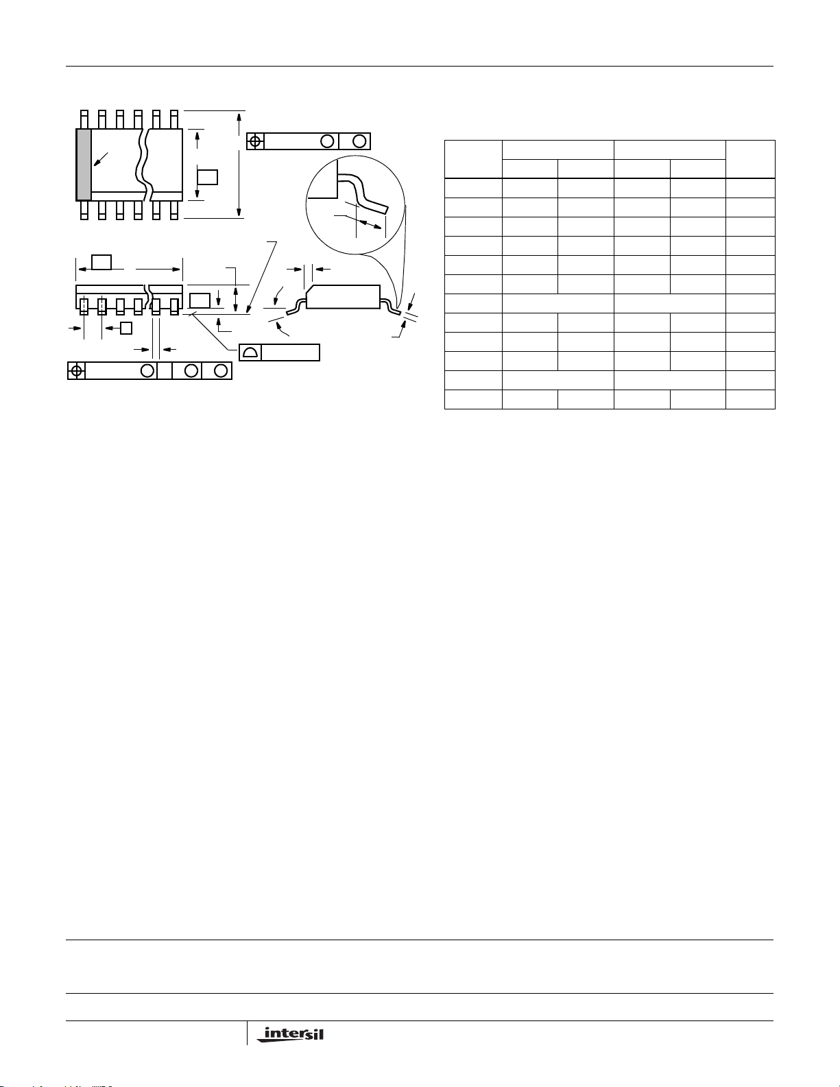
Quad Flat No-Lead Plastic Package (QFN)
Micro Lead Frame Plastic Package (MLFP)
L20.5x5
20 LEAD QUAD FLAT NO-LEAD PLASTIC PACKAGE
MILLIMETERS
SYMBOL
A 0.80 0.90 1.00 A1 - 0.02 0.05 A2 - 0.65 1.00 9
A3 0.20 REF 9
b 0.23 0.30 0.38 5, 8
D 5.00 BSC D1 4.75 BSC 9
D2 2.95 3.10 3.25 7, 8
E 5.00 BSC E1 4.75 BSC 9
E2 2.95 3.10 3.25 7, 8
e 0.65 BSC -
k0.20 - - -
L 0.35 0.60 0.75 8
N202
Nd 5 3
Ne 5 3
P- -0.609
θ --129
NOTES:
1. Dimensioning and tolerancing conform to ASME Y14.5-1994.
2. N is the number of terminals.
3. Nd and Ne refer to the number of terminals on each D and E.
4. All dimensions are in millimeters. Angles are in degrees.
5. Dimension b applies to the metallized terminal and is measured
between 0.15mm and 0.30mm from the terminal tip.
6. The configuration of the pin #1 identifier is optional, but must be
located within the zone indicated. The pin #1 identifier may be
either a mold or mark feature.
7. Dimensions D2 and E2 are for the exposed pads which provide
improved electrical and thermal performance.
8. Nominal dimensions are provided to assist with PCB Land Pattern
Design efforts, see Intersil Technical Brief TB389.
9. Features and dimensions A2, A3, D1, E1, P & θ are present when
Anvil singulation method is used and not present for saw
singulation.
10. Compliant to JEDEC MO-220VHHC Issue I except for the "b"
dimension.
NOTESMIN NOMINAL MAX
Rev. 4 11/04
16
Page 17
Small Outline Plastic Packages (SOIC)
www.BDTIC.com/Intersil
ISL6505
N
INDEX
AREA
123
-A-
0.25(0.010) B
E
SEATING PLANE
D
-C-
H
-B-
A
M
L
M
h x 45°
α
e
B
0.25(0.010) C AMB
NOTES:
1. Symbols are defined in the “MO Series Symbol List” in Section
2.2 of Publication Number 95.
2. Dimensioning and tolerancing per ANSI Y14.5M-1982.
3. Dimension “D” does not include mold flash, protrusions or gate
burrs. Mold flash, protrusion and gate burrs shall not exceed
0.15mm (0.006 inch) per side.
4. Dimension “E” does not include interlead flash or protrusions.
Interlead flash and protrusions shall not exceed 0.25mm (0.010
inch) per side.
5. The chamfer on the body is optional. If it is not present, a visual
index feature must be located within the crosshatched area.
6. “L” is the length of terminal for soldering to a substrate.
7. “N” is the number of terminal positions.
8. Terminal numbers are shown for reference only.
9. The lead width “B”, as measured 0.36mm (0.014 inch) or greater
above the seating plane, shall not exceed a maximum value of
0.61mm (0.024 inch)
10. Controlling dimension: MILLIMETER. Converted inch
dimensions are not necessarily exact.
M
A1
0.10(0.004)
S
M20.3 (JEDEC MS-013-AC ISSUE C)
20 LEAD WIDE BODY SMALL OUTLINE PLASTIC PACKAGE
INCHES MILLIMETERS
SYMBOL
A 0.0926 0.1043 2.35 2.65 -
A1 0.0040 0.0118 0.10 0.30 -
B 0.014 0.019 0.35 0.49 9
C 0.0091 0.0125 0.23 0.32 -
D 0.4961 0.5118 12.60 13.00 3
E 0.2914 0.2992 7.40 7.60 4
e 0.050 BSC 1.27 BSC -
H 0.394 0.419 10.00 10.65 -
C
h 0.010 0.029 0.25 0.75 5
L 0.016 0.050 0.40 1.27 6
N20 207
α
0° 8° 0° 8° -
NOTESMIN MAX MIN MAX
Rev. 2 6/05
All Intersil U.S. products are manufactured, assembled and tested utilizing ISO9000 quality systems.
Intersil Corporation’s quality certifications can be viewed at www.intersil.com/design/quality
Intersil products are sold by description only. Intersil Corporation reserves the right to make changes in circuit design, software and/or specifications at any time without
notice. Accordingly, the reader is cautioned to verify that data sheets are current before placing orders. Information furnished by Intersil is believed to be accurate and
reliable. However, no responsibility is assumed by Intersil or its subsidiaries for its use; nor for any infringements of patents or other rights of third parties which may result
from its use. No license is granted b y implica tion or ot herw ise un der any patent or patent rights of Intersil or its subsidiaries.
For information regarding Intersil Corporation and its products, see www.intersil.com
17
 Loading...