

Page 1
Application Note 1181
Author: Pengju Kong
ISL6442 Dual PWM and Linear Controller Evaluation
Board User Guide
This application note describes how to use the ISL6442EVAL1Z
(Rev. C) board to evaluate the ISL6442 dual switching
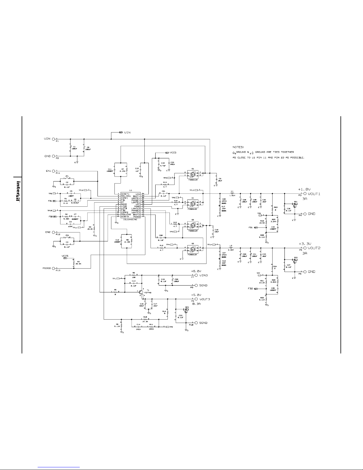
regulator, plus one linear regulator. Refer to the schematic,
BOM (Bill of Materials), and board layout (at the end of this
document), as needed. The ISL6442 datasheet
is also used as
a reference.
Configuration
The outputs are set up as follows:
•Switcher V
•Switcher V
•Linear V
The outputs are switching at ~1.4MHz rate, based on the
resistor selected on the RT pin.
The current range for the switcher output that is presently
supported is limited by the FETs used. The FDS6912A dual FET
(in SO-8 package) can handle up to 3A. However, the ISL6442
gate drivers are capable of driving discrete upper and lower
FETs for up to 25A output current as well, even though not
supported on this board.
The linear output supports ~1W. The output current capability
of the linear regulator is determined mainly by the power
dissipation of the FET as mounted:
PV
= (V
OUT3
= 1.8V @ 3A (with VIN = 6V)
OUT1
= 3.3V @ 3A (with VIN = 6V)
OUT2
= 5.0V @ 0.3A (with V
OUT3
IN3-VOUT3
)*I
OUT3
= 6V)
IN3
.
Quick Start Evaluation
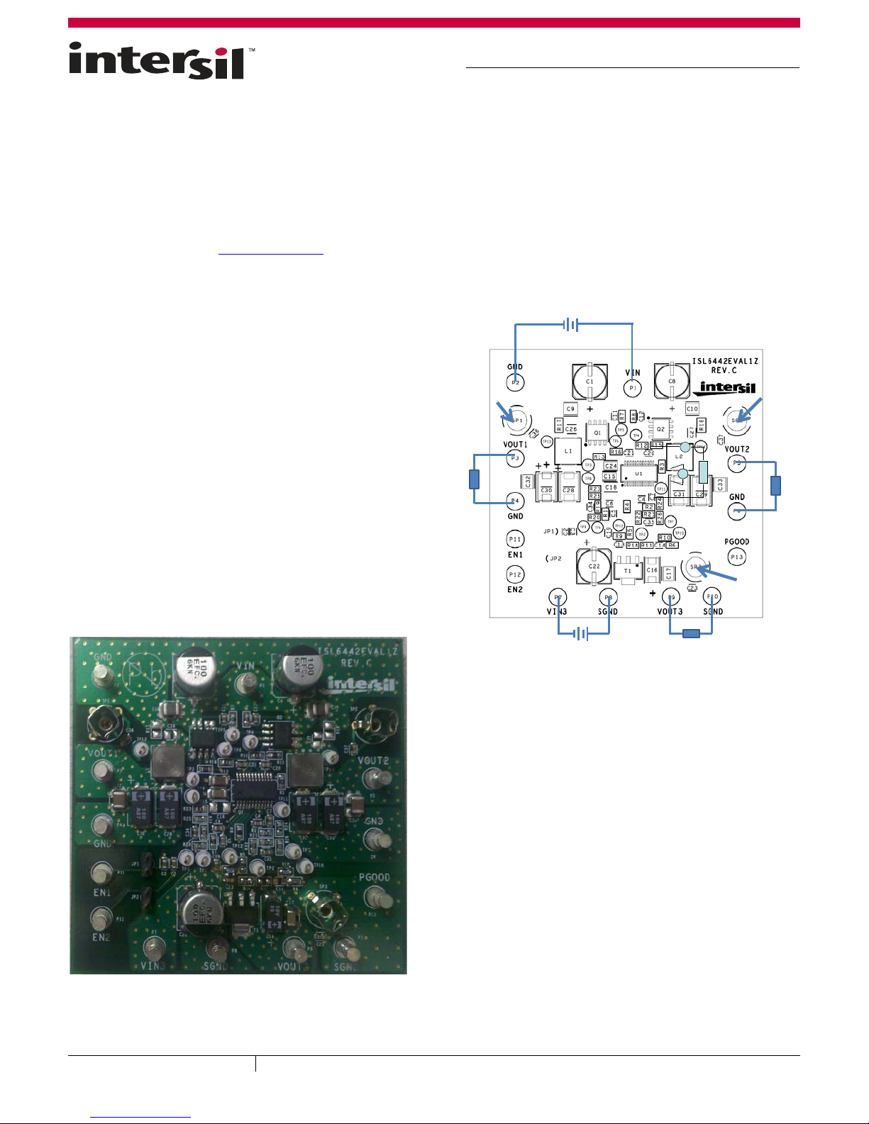
Figure 1 shows a photo of the populated board, and Figure 2
shows a plot of the top layer for reference, and details the
available input and output connections. Two switchers share
one input V
input (V
GND, plus a scope probe socket, for low noise waveforms.
V
OUT1
test
point
V
OUT1
. The linear regulator has separate turrets for its
IN
) and GND. Each output has turrets for VOUT and
IN3
VIN= 6V
I
out
A
LOAD
+
VV
_
V
out
LOAD
V
OUT2
V
OUT2
test
point
LOAD
FIGURE 1. ISL6442EVAL1Z BOARD PHOTO
V
= 6V V
IN3
FIGURE 2. ISL6442EVAL1Z INPUT AND OUTPUT CONNECTIONS
OUT3
LOAD
Quick Start Setup (Light Load)
For a quick and easy test, one 6V supply is needed. Connect P1
(V
) and P7 (V
IN
) to each other, and to the 6V supply; connect
IN3
the supply GND to P2 and P9. Attach light loads to each
output.
Switch on the power supply; all three outputs should turn on to
their expected DC values; use a voltmeter or oscilloscope to
view them. VOUT1 and VOUT2 will have a ramp time of a few
milliseconds (VOUT3 will be much faster).
Note that the IC and all three inputs are sharing one supply
voltage in this simple example. The linear V
can certainly be
IN3
different, since it has its own input posts.
Board Features and Modifications
Heavier loads can be evaluated by placing them across the
appropriate output to GND. Resistors, electronic loads, or
November 28, 2011
AN1181.1
1
1-888-INTERSIL or 1-888-468-3774
CAUTION: These devices are sensitive to electrostatic discharge; follow proper IC Handling Procedures.
| Intersil (and design) is a trademark owned by Intersil Corporation or one of its subsidiaries.
All other trademarks mentioned are the property of their respective owners.
Copyright Intersil Americas Inc. 2011. All Rights Reserved.
Page 2
Application Note 1181
actual loads can be used. It is STRONGLY recommended that the
power be turned off when attaching loads, due to the tight
spacing of the posts. The switcher outputs should be able to
provide at least 3A; monitor the FET temperature if you try to go
higher, to be sure the conditions will allow it. Make sure the input
power supply can source the amount of input current necessary
to drive the maximum loads to be tested.
The linear VOUT3 is especially sensitive to power dissipation
concerns; it will change as the user varies either the input
voltage, the output voltage, and/or the load current. The
equation used is PV
OUT3
= (V
IN3-VOUT3
)*I
. The PNP bipolar
OUT3
will also be rated for how well the power is dissipated from the
package and spread out on the board; this is another variable
that the user must keep in mind for their design and layout.
JP1 is used to disable VOUT1, by shorting SS/EN1 to GND. JP2
does the same function for VOUT2.
The switching frequency is controlled by a resistor (R4) on the RT
pin, to GND. Refer to the datasheet for the curve of resistor
values versus frequency.
Each output voltage is determined by a resistor divider from the
output to its FB pin to GND. See the ISL6442 datasheet
for the
formulas to calculate the values. Note that there are some
limitations; the switchers can approach 100% duty, but will be
limited by dead time, r
of the FETs at maximum load,
DSON
switching frequency, etc. The maximum values are limited by the
VIN available (if you want go higher, check the ratings of the FETs,
and other output components to be sure they can handle it). The
minimum output voltage will be just above the 0.6V internal
reference. The maximum output voltage for the linear is limited
by the VIN3 and the LCDR pin (which is biased from 5V). Thus, the
maximum output voltage is close to the 5V set on the board; it is
not recommended to go higher. The minimum voltage will also
be just above the 0.6V internal reference.
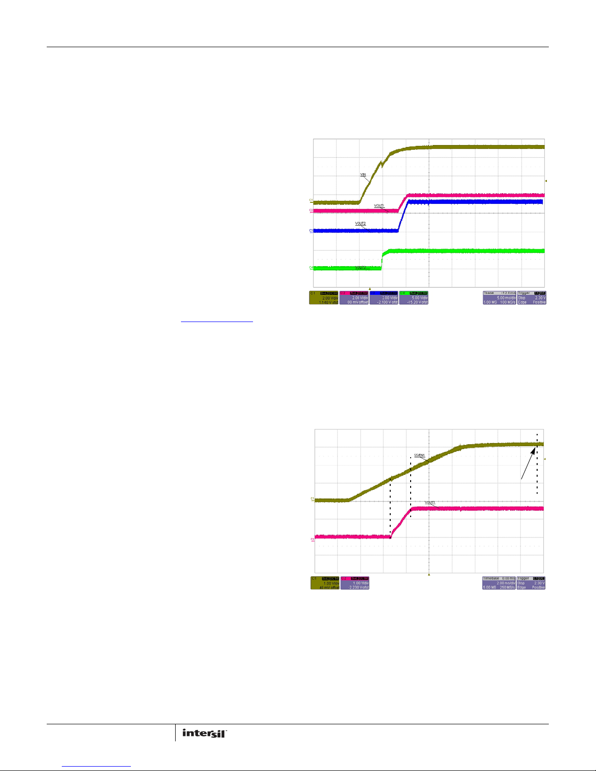
start their soft-start ramps at the same time. In this case, both
outputs track each other initially; this is accomplished by
selecting the ratio of SS/EN capacitors to match their output
voltages. The ramp times shown are on the order of a few
milliseconds, as determined by the SS/EN capacitors on the
board.
CH1 VIN
(2V/DIV)
CH2 VOUT1
(2V/DIV)
CH3 VOUT2
(2V/DIV)
CH4 VOUT3
(5V/DIV)
5ms/DIV; VIN3 = VIN
FIGURE 3. TYPICAL POWER-UP WAVEFORMS WITH VIN
Figure 4 shows the detail soft start waveform of PWM1 (PMW2
would be similar). The full SS/EN1 ramp is shown; the output
doesn’t start to ramp until the SS/EN passes the ~1V threshold
for Enable. The output ramps from zero to full scale, while
SS/EN1 ramps from 1.0V to 1.6V. Finally, the EN/SS1 keeps
ramping up to ~3.2V, at which point the ramp is considered done
(the PGOOD timer would start from this point, if both outputs
ramps were done).
CH1 EN/SS1
(1V/DIV)
Performance Waveforms
These figures depict the ISL6442EVAL1Z performance during
typical operational situations, as well as during fault conditions.
Loading of the output can be most easily done via an electronic
load; however, other methods can work as well.
Figure 3 shows a typical power-up sequence, with all inputs
connected to a single VIN = VIN3 = 6V. When VCC exceeds its
POR rising trip point (~4.4V), the IC is enabled, and the linear
VOUT3 comes up almost immediately. Meanwhile, the two SS/EN
pins start charging (not shown), but the outputs do not start
ramping until the SS/EN pins ~1V; then both switcher outputs
2
2ms/DIV
FIGURE 4. PWM1 SOFT-START
~3.2V
CH1 OUT1
(1V/DIV)
November 28, 2011
AN1181.1
Page 3
Application Note 1181
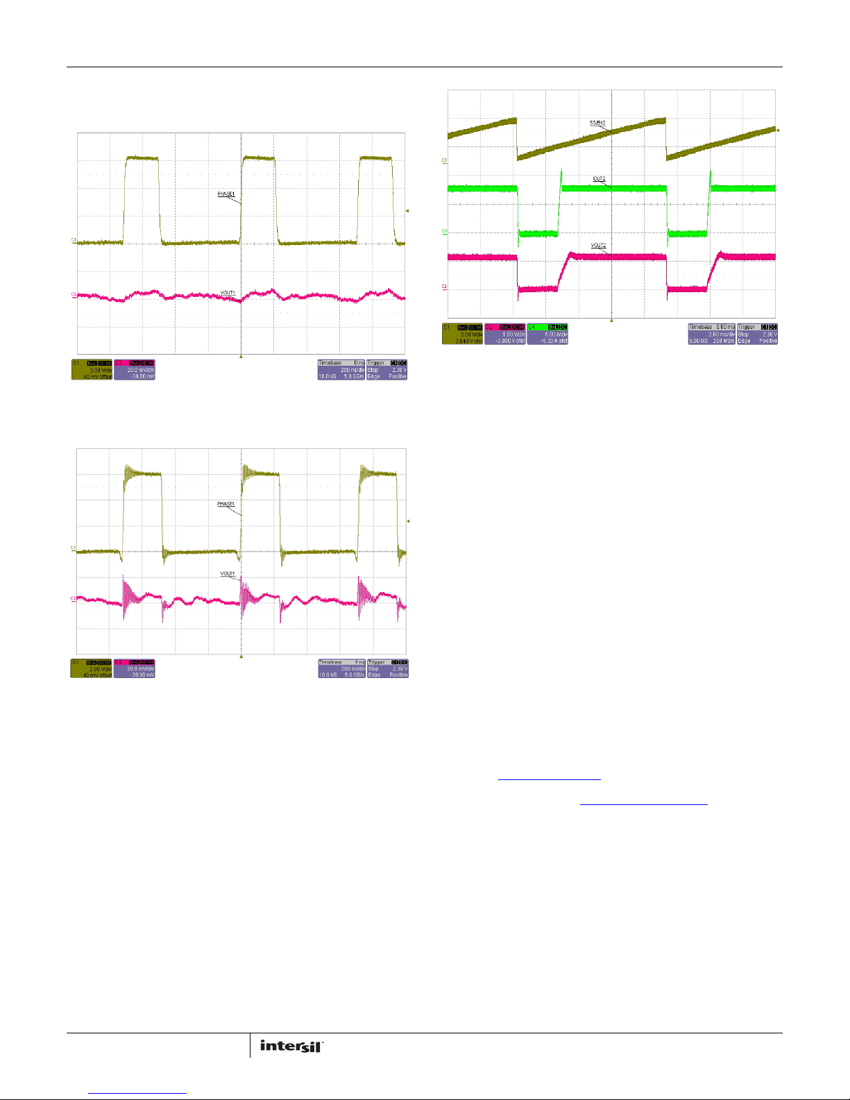
Figures 5 and 6 show the PHASE1 signal (which has the same
timing as UGATE1) and the output voltage ripple on VOUT1 at no
load and 3A load. The switching frequency is 1.4 MHz.
CH1
SS/EN2
(2V/DIV)
CH1
PHASE1
(2V/DIV)
CH2 (AC)
VOUT1
(20mV/DIV)
0.2µs/DIV; VOUT1 = 1.8V; VIN = 6V
FIGURE 5. PWM1 SWITCHING AND RIPPLE WAVEFORMS AT
NO LOAD
CH1
PHASE1
(2V/DIV)
CH4
I
LOAD2
(5A/DIV)
CH2
VOUT2
(1V/DIV)
T0 T1
2ms/DIV; VOUT2 = 3.3V; VIN = 6V; ROCSET = 2.15kW
FIGURE 7. PWM2 OVERCURRENT HICCUP MODE
Conclusion
The ISL6442EVAL1Z evaluation board showcases a simple, but
high-performance dual regulator, providing control in a variety of
applications, with emphasis on computer systems. The
high-current MOSFET drivers of the ISL6442 yield a highly
efficient power conversion solution with a reduced number of
external components in a compact footprint.
Documentation
See the following pages for more detailed information, including:
CH2 (AC)
VOUT1
(20mV/DIV)
0.2µs/DIV; VOUT1 = 1.8V; VIN = 6V
FIGURE 6. PWM1 SWITCHING AND RIPPLE WAVEFORMS
AT 3 A L OA D
Figure 7 shows the overcurrent hiccup mode already in
operation. At time T0, the SS/EN2 is discharged to GND (it may
not have time to reach GND, due to the limited size of the
discharge transistor, plus the size of the timing capacitor). Once
SS/EN2 is below ~1V, the output should shut off, and the load
current goes to zero; this occurs by time T1. Once SS/EN2 rises
above 1V again, the VOUT2 will try to turn on again. If the output
remains shorted, the output current will be limited on each clock
cycle to an average value low enough to keep the dissipation
reasonable.
• “Schematic” of ISL6442EVAL1Z
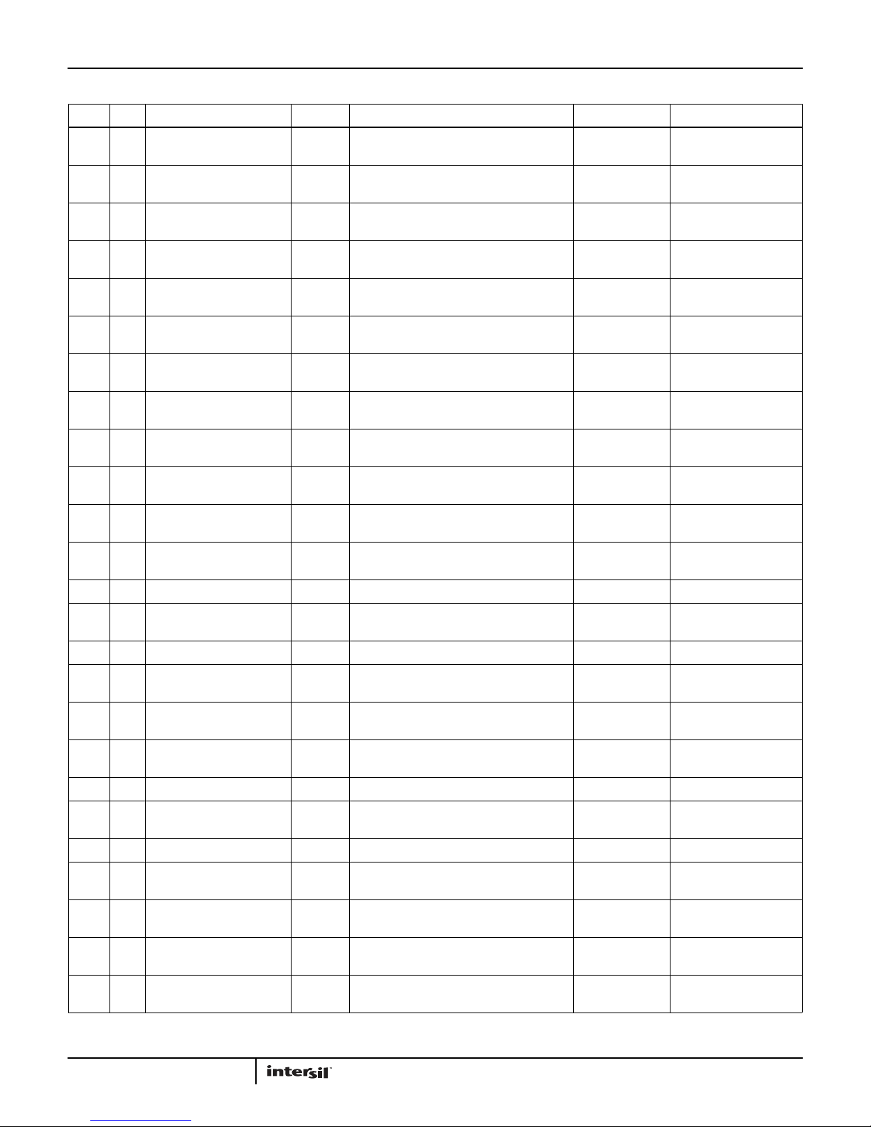
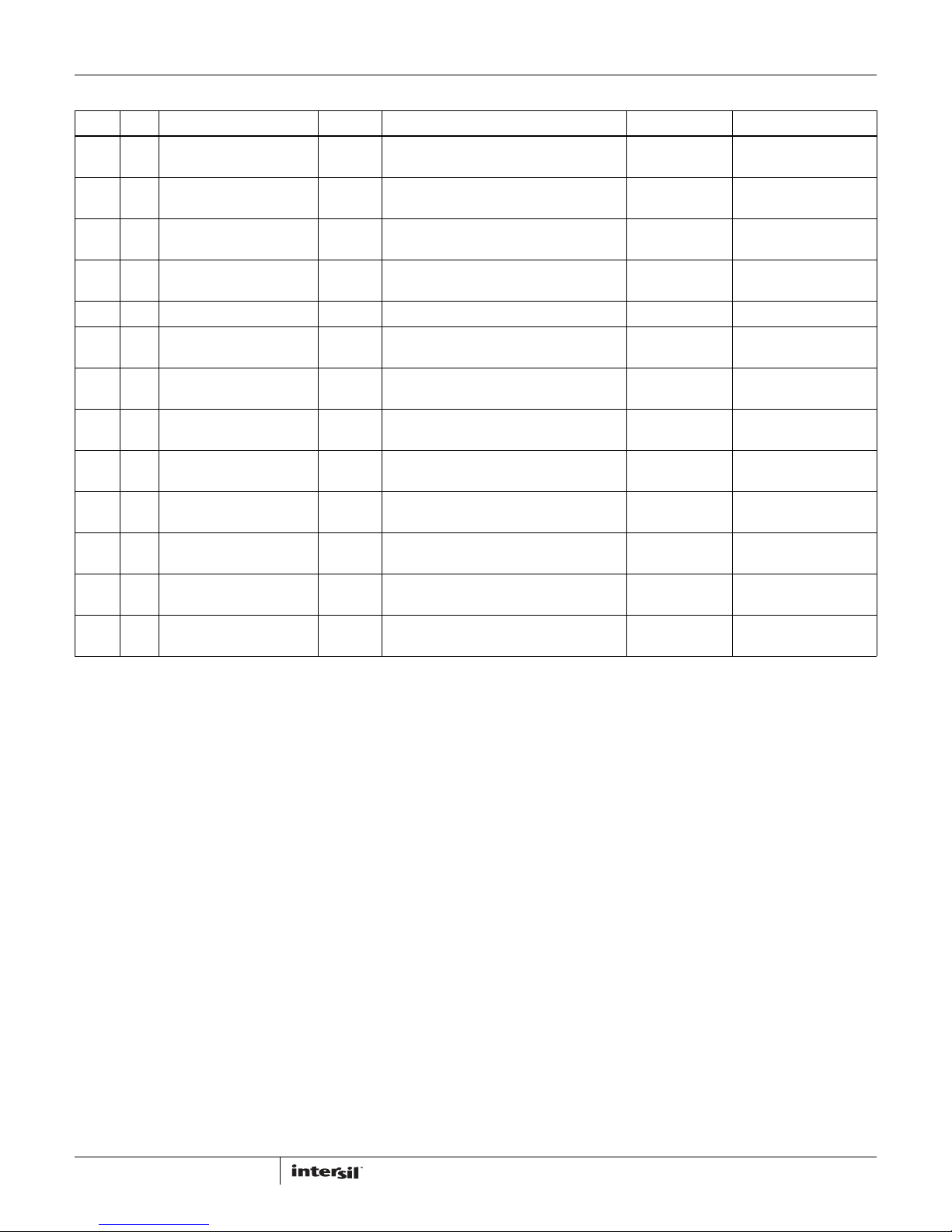
• Table 1, “BILL OF MATERIALS” on page 5
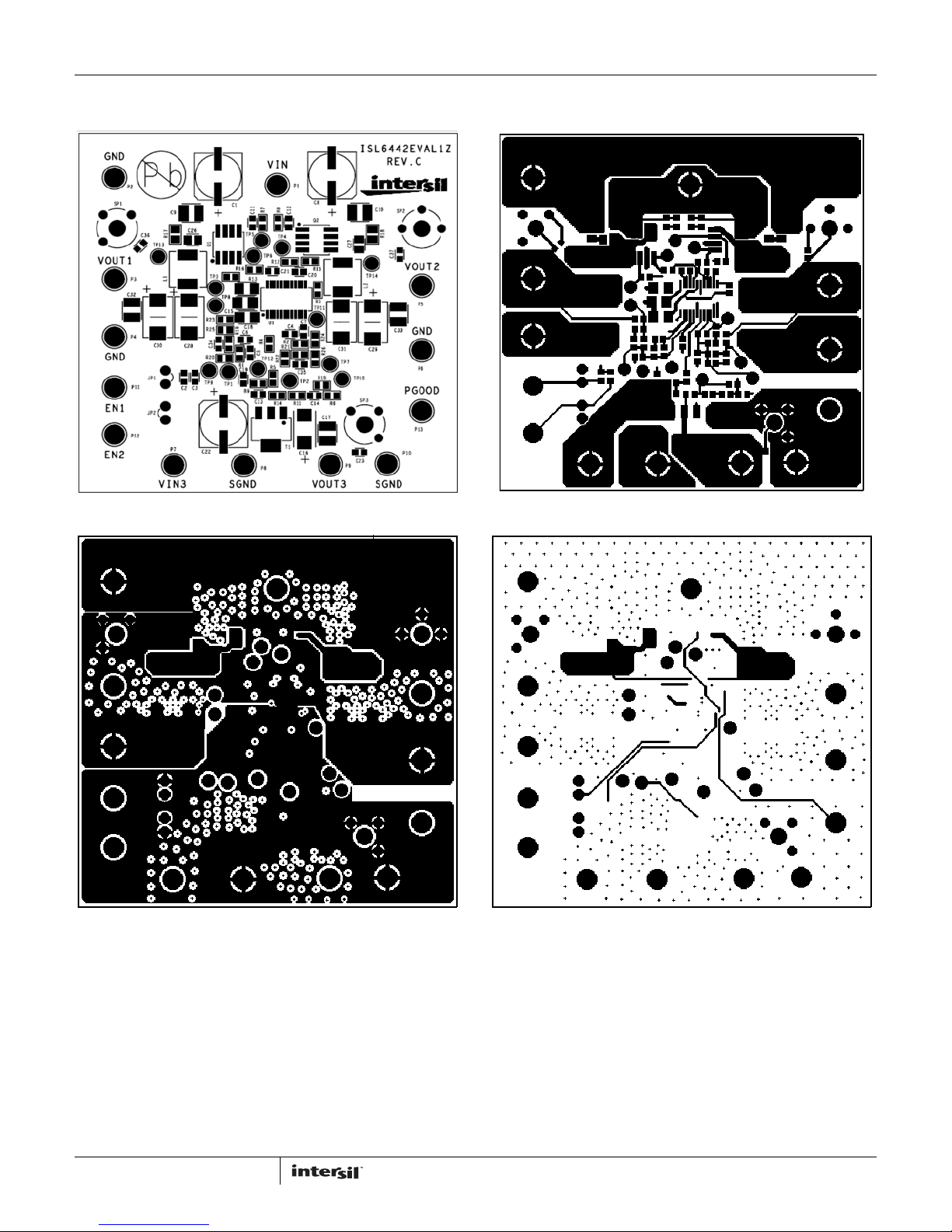
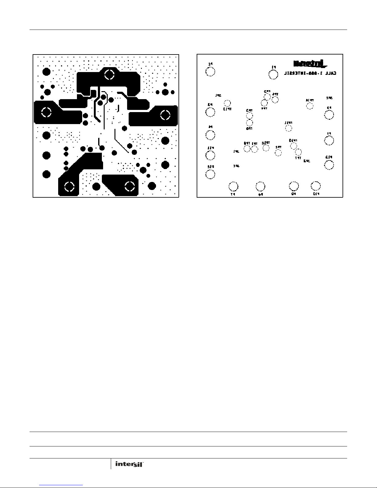
• “ISL6442EVAL1Z Board Layout” on page 7. Note that this
board layout has not been fully optimized for performance or
minimum board area, primarily due to the various options, test
points, and other features to make testing easier. So while it
follows most of the recommended practices, it could
potentially be improved for any given single application.
References
Datasheet: ISL6442 datasheet
Visit us on the internet, at: http://www.intersil.com
3
November 28, 2011
AN1181.1
Page 4
Application Note 1181
4
AN1181.1
November 28, 2011
Schematic
SGND
AS CLOSE TO U1 PIN 11 AND PIN 23 AS POSSIBLE.
+1.8V
+3.3V
GND
GND
3A
GROUND & GROUND ARE TIED TOGETHER
NOTES:
SGND
+5.0V
0.3A
GND
3A
+6.0V
VIN
01/24/2007
THEJU BERNARD
6.04K
C24
OPEN
C18
2
1
R16
4.7
1
1
TP11
1
TP10
1
TP9
1
1
TP13
2
1
C14
2
1
R5
2
1
C16
2
1
R11
2
1
C19
2
1
C22
2
1
C17
2
1
C13
2
1
R9
2
1
R6
2
1
R10
2
1
R4
2
1
C3
2
1
1
C29
2
C28
2
1
C31
2
1
C30
2
1
C33
1
R21
2
1
R22
2
1
2
1
C35
1
C34
2
1
R25
2
1R22
1
C7
2
1
C4
2
1
C6
2
1
C5
2
1
R1
2
1
R19
1
2
1
2
1
R12
1
P13
2
1
R3
1
P12
1
P11
2
1
R8
2
1
C12
2
2
R18
2
1
2
1
C26
2
1
2
1
C20
2
1
C21
2
1
C23
2
1
C37
2
1
C36
2
1
2
1
19
15
11
2
6
5
13
18
12
1
17
20
8
7
9
4
10
3
14
2
1
R23
2
1
R24
2
1
R14
1
TP2
1
TP7
1
TP4
1
TP6
1
TP1
1
P8
2
1
JP1
2
1
JP2
1
432
SP2
1
432
SP1
1
432
SP3
1
P9
3
42
1
T1
1
2
8
7
Q2
4
6
5
Q2
4
6
5
Q1
1
2
8
7
Q1
1
P10
1
1
P4
1
P6
1
P1
1
P7
1
P3
1
5.11K
VOUT1
FDS6912A
VIN
EVALUATION BOARD
1
1
TIM KLEMANN
SCHEMATIC
ISL6442EVAL1Z
C
~/ISL6442/ISL6442EVAL1ZC
ISL6442
FB1
FB1
3.24K
0
10.5K
0
5.11K
23.2K
1000PF
DNP
10.2K
0.015UF
0.1UF
EN1
5.49K
ISL6442IAZ
DNP
OPEN
0805
100UF
100UF
10UF
100UF
10UF
OPEN
VOUT2
0.1UF
10UF
8200PF
100PF
0.1UF
1000PF
2.15K
PGOOD
VCC5
EN2
4.7
36.5K
FB2
1.5UH
2.1K
5.11K
0
OPEN
68UF 10UF
0
0.1UF
0.1UF
100
FZT749
0.1UF
100UF
VOUT3
0.1UF
OPEN
37.4K
0.1UF
4.7
47PF
TP8
2
0805
3
16
0805
1
2
U1
21
22
24
0805
R17
TP5
L1
L2
2
P2
1
0.1UF
C9
C10
100UF
C8
1
2
100UF
C1
1
2
2
1
1UF
C15
R13
4.7
1
2
TP3
1
VCC5
4.7UF
1
2
R7
1
C11
1000PF
2.15K
2
P5
10UF
2
R26
C27
TP12
1
2.2UH
TP14
FB2
1500PF
2
R20
VIN3
FDS6912A
3
FDS6912A
FDS6912A
23
C2
1
100UF
R15
1
C32
1
E
EE
E
E
E
D
D
D
D
E
D
D
G
S
D
D
G
S
E
D
D
G
S
D
D
G
S
E
E
D
E
D
E
E
E
D
D
D
D
D
OCSET1
SS1/EN1
BOOT1
VIN
UGATE1
PHASE1
LGATE1
VCC
PGND
LGATE2
PHASE2
UGATE2
BOOT2
PGOOD
OCSET2
SS2/EN2
COMP2
FB2
LCFB
LCDR
SGND
RT
COMP1
FB1
E
E
E
D
D
OUT
IN
OUT
IN
IN
OUT
OUT
FILENAME:
OF
SHEET
REV.
DATE:
HRDWR ID
MASK#
TITLE:
ENGINEER:
DATE:
DATE:
DATE:
TESTER
UPDATED BY:
RELEASED BY:
DRAWN BY:
E
D
C
B
A
7
654
3
2
1
E
D
C
B
A
FF
8
Page 5
Application Note 1181
TABLE 1. BILL OF MATERIALS
ITEM QTY PART REFERENCE VALUE DESCRIPTION PART # MANUFACTURER
1 4 C28-C31 100µF CAP-TANT LOWESR, SMD, D3, 100µF, 10V,
20%, POSCAP, ROHS
2 1 C16 68µF CAP, SMD, 6x3.2, 68µF, 10V, 20% POSCAP,
ROHS
3 4 C2, C3, C13, C19 0.1µF CAPACITOR, SMD, 0603, 0.10µF, 50V, 10%,
X7R
4 1 C18 4.7µF CAPACITOR, SMD, 1206, 4.7µF, 16V, 10%,
X7R, ROHS
5 3 C17, C32, C33 10µF CAP, SMD, 1210, 10µF, 25V, 20%, X7R,
ROHS
6 3 C1, C8, C22 100µF CAP, SMD, 8X10.2, 100µF, 25V, 20%, AL.EL,
ROHS
7 2 C9, C10 10µF CAP, SMD, 1210, 10µF, 35V, 10%, X5R,
ROHS
8 1 C5 100pF CAP, SMD, 0603, 100pF, 50V, 5%, COG,
ROHS
9 3 C11, C12, C35 1000pF CAP, SMD, 0603, 1000pF, 50V, 10%, X7R,
ROHS
10 5 C20, C21, C23, C36, C37 0.1µF CAP, SMD, 0603, 0.1µF, 25V, 10%, X7R,
ROHS
11 1 C34 1500pF CAP, SMD, 0603, 1500pF, 50V, 10%, X7R,
ROHS
12 1 C6 15nF CAP, SMD, 0603, .015µF, 50V, 10%, X7R,
ROHS
13 1 C4 47pF CAP, SMD, 0603, 47pF, 50V, 5%, NPO, ROHS Generic
14 1 C7 8200pF CAP, SMD, 0603, 8200pF, 50V, 10%, X7R,
ROHS
15 1 C15 1µF CAP, SMD, 1206, 1µF, 50V, 10%, X7R, ROHS Generic
16 1 L1 1.5µH COIL-PWR INDUCTOR, SMD, 6.9x6.5m,
1.5µH, 20%, 9A, ROHS
17 1 L2 2.2µH COIL-PWR INDUCTOR, SMD, 6.9x6.5m,
2.2µH, 20%, 10A, ROHS
18 3 SP1-SP3 CONN-SCOPE PROBE TEST PT, COMPACT,
PCB MNT, ROHS
19 13 P1-P13 CONN-TURRET, TERMINAL POST, TH, ROHS 1514-2 1514-2
20 14 TP1-TP14 CONN-MINI TEST POINT, VERTICAL, WHITE,
ROHS
21 2 JP1, JP2 CONN-JUMPER, 2PIN, SHUNT, ROHS SPC02SYAN SPC02SYAN
22 1 U1 IC-PWM/LINEAR CONTROLLER, 24P, QSOP,
ROHS
23 2 Q1, Q2 TRANSIST-DUAL MOS, N-CHAN, 8P, SOIC,
30V, 6A, ROHS
24 1 T1 TRANSISTOR, PNP, SMD, SOT223, -25V, -3A,
ROHS
25 4 R12, R13, R15, R16 4.7Ω RES, SMD, 0603, 4.7Ω, 1/10W, 1%, TF,
ROHS
10TPB100M SANYO
10TPB68MC SANYO
Generic
Generic
Generic
EEE-FC1E101P EEE-FC1E101P
Generic
Generic
Generic
Generic
Generic
Generic
Generic
IHLP-2525CZ-ER-
1R5-M01
IHLP-2525CZ-ER-
2R2-M01
131-4353-00 131-4353-00
5002 5002
ISL6442IAZ ISL6442IAZ
FDS6912A FDS6912A
FZT749 FZT749
IHLP-2525CZ-ER-1R5-
M01
IHLP-2525CZ-ER-2R2-
M01
Generic
5
November 28, 2011
AN1181.1
Page 6
Application Note 1181
TABLE 1. BILL OF MATERIALS
ITEM QTY PART REFERENCE VALUE DESCRIPTION PART # MANUFACTURER
26 4 R5, R14, R23, R24 0Ω RESISTOR, SMD, 0603, 0Ω, 1/10W, TF,
ROHS
27 1 R9 100Ω RES, SMD, 0603, 100Ω, 1/10W, 1%, TF,
ROHS
28 1 R4 10.2kΩ RES, SMD, 0603, 10.2k, 1/10W, 1%, TF,
ROHS
29 1 R19 10.5kΩ RES, SMD, 0603, 10.5k, 1/10W, 1%, TF,
ROHS
30 1 R1 2.1kΩ RES, SMD, 0603, 2.1k, 1/10W, 1%, TF, ROHS Generic
31 2 R7, R8 2.15kΩ RES, SMD, 0603, 2.15k, 1/10W, 1%, TF,
ROHS
32 1 R21 23.2kΩ RES, SMD, 0603, 23.2k, 1/10W, 1%, TF,
ROHS
33 1 R25 3.24kΩ RES, SMD, 0603, 3.24k, 1/10W, 1%, TF,
ROHS
34 1 R3 36.5kΩ RES, SMD, 0603, 36.5k, 1/10W, 1%, TF,
ROHS
35 1 R10 37.4kΩ RES, SMD, 0603, 37.4k, 1/10W, 1%, TF,
ROHS
36 3 R6, R20, R22 5.11kΩ RES, SMD, 0603, 5.11k, 1/10W, 1%, TF,
ROHS
37 1 R2 5.49kΩ RES, SMD, 0603, 5.49k, 1/10W, 1%, TF,
ROHS
38 1 R26 6.04kΩ RES, SMD, 0603, 6.04k, 1/10W, 1%, TF,
ROHS
(Continued)
Generic
Generic
Generic
Generic
Generic
Generic
Generic
Generic
Generic
Generic
Generic
Generic
6
November 28, 2011
AN1181.1
Page 7
Application Note 1181
ISL6442EVAL1Z Board Layout
FIGURE 8. TOP SILKSCREEN FIGURE 9. TOP LAYER
FIGURE 10.2ND LAYER FIGURE 11.3RD LAYER
7
November 28, 2011
AN1181.1
Page 8
Application Note 1181
ISL6442EVAL1Z Board Layout (Continued)
FIGURE 12. BOTTOM LAYER
FIGURE 13. BOTTOM SILKSCREEN
Intersil Corporation reserves the right to make changes in circuit design, software and/or specifications at any time without notice. Accordingly, the reader is
cautioned to verify that the Application Note or Technical Brief is current before proceeding.
For information regarding Intersil Corporation and its products, see www.intersil.com
8
November 28, 2011
AN1181.1
Page 9

Mouser Electronics
Authorized Distributor
Click to View Pricing, Inventory, Delivery & Lifecycle Information:
Intersil:
ISL6442EVAL1Z
 Loading...