®
www.BDTIC.com/Intersil
ISL6425
Data Sheet
Single Output LNB Supply and Control
Voltage Regulator with I2C Interface for
Advanced Satellite Set-top Box Designs
The ISL6425 is a highly integrated solution for supplying
power and control signals from advanced satellite set-top
box (STB) modules to the low noise block (LNB). This device
is comprised of a current-mode boost PWM and a low-noise
linear regulator, along with the circuitry required for I
device interfacing and for providing DiSEqC standard control
signals to the LNB.
A regulated output voltage is available at the output terminal
(VOUT) to support the operation of the antenna port in
advanced satellite STB applications. The regulated output
may be set to either 13V or 18V by use of the voltage select
command (VSEL) through the I
compensate for the voltage drop in the coaxial cable, the
voltage may be increased by 1V with the line length
compensation (LLC) feature. An enable command sent on
2
the I
C bus provides standby mode control for the PWM and
linear combination, disabling the output to conserve power.
A current-mode boost converter provides the linear regulator
with an input voltage that is set to the required output
voltage, plus 1.2V (typ.) to insure minimum power
dissipation. This maintains a constant voltage drop across
the linear pass element, while permitting an adequate
voltage range for tone injection.
The device is capable of providing 750mA (typ.).
2
C bus. Additionally, to
2
C
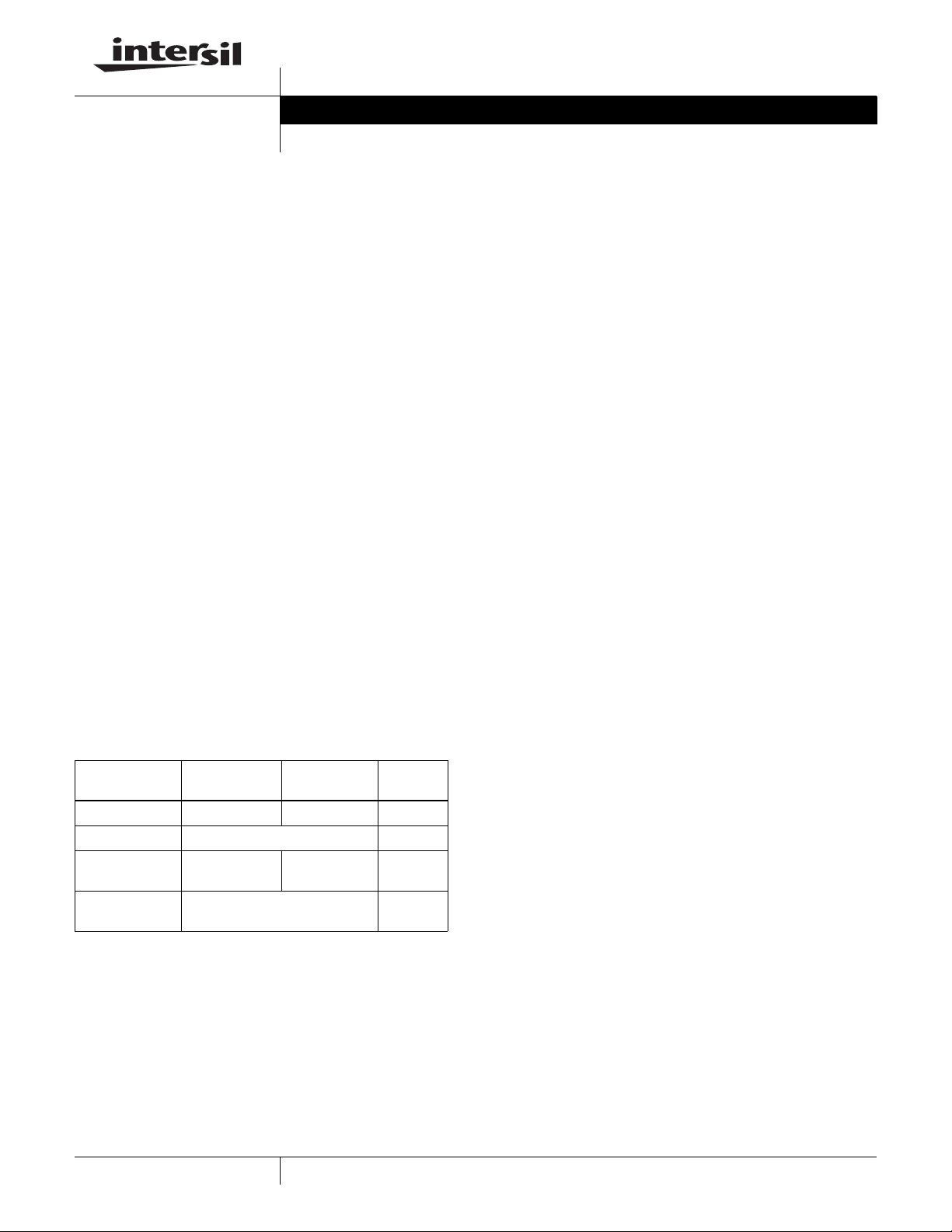
Ordering Information
TEMP.
PART NUMBER
ISL6425ER -20 to 85 32 Ld 5x5 QFN L32.5x5
ISL6425ER-T 32 Ld 5x5 QFN Tape and Reel L32.5x5
ISL6425ERZ
(Note)
ISL6425ERZ-T
(Note)
NOTE: Intersil Pb-free products employ special Pb-free material sets;
molding compounds/die attach materials and 100% matte tin plate
termination finish, which are RoHS compliant and compatible with
both SnPb and Pb-free soldering operations. Intersil Pb-free products
are MSL classified at Pb-free peak reflow temperatures that meet or
exceed the Pb-free requirements of IPC/JEDEC J STD-020.
RANGE (°C) PACKAGE
-20 to 85 32 Ld 5x5 QFN
(Pb-free)
32 Ld 5x5 QFN Tape and Reel
(Pb-free)
PKG.
DWG. #
L32.5x5
L32.5x5
February 8, 2005
FN9176.1
Features
• Switch-Mode Power Converter for Lowest Dissipation
- Boost PWM with >92% Efficiency
- Selectable 13V or 18V Outputs
- Digital Cable Length Compensation (1V)
• External Pin to Select 13V/18V Options
• DSQIN and SEL18V pins are 2.5V logic compatible
2
C Compatible Interface for Remote Device Control
•I
- Registered Slave Address 0001 00XX
- Fully Functional 3.3V, 5V Operation up to 400kHz
• Built-In Tone Oscillator Factory Trimmed to 22kHz
- Facilitates DiSEqC (EUTELSAT) Encoding
• Internal Over-Temperature Protection and Diagnostics
2
• Internal Overload and Overtemp Flags (Visible on I
• LNB Short-Circuit Protection and Diagnostics
• QFN Package
- Compliant to JEDEC PUB95 MO-220 QFN - Quad Flat
No Leads - Product Outline
- Near Chip-Scale Package Footprint
• Pb-free available (RoHS Compliant)
C)
Applications
• LNB Power Supply and Control for Satellite Set-Top Box
References
• Tech Brief 389 (TB389) - “PCB Land Pattern Design and
Surface Mount Guidelines for QFN Packages”; Available
on the Intersil website, www.intersil.com
1
CAUTION: These devices are sensitive to electrostatic discharge; follow proper IC Handling Procedures.
1-888-INTERSIL or 321-724-7143
All other trademarks mentioned are the property of their respective owners.
| Intersil (and design) is a trademark of Intersil Americas Inc.
Copyright © Intersil Americas Inc. 2004-2005. All Rights Reserved

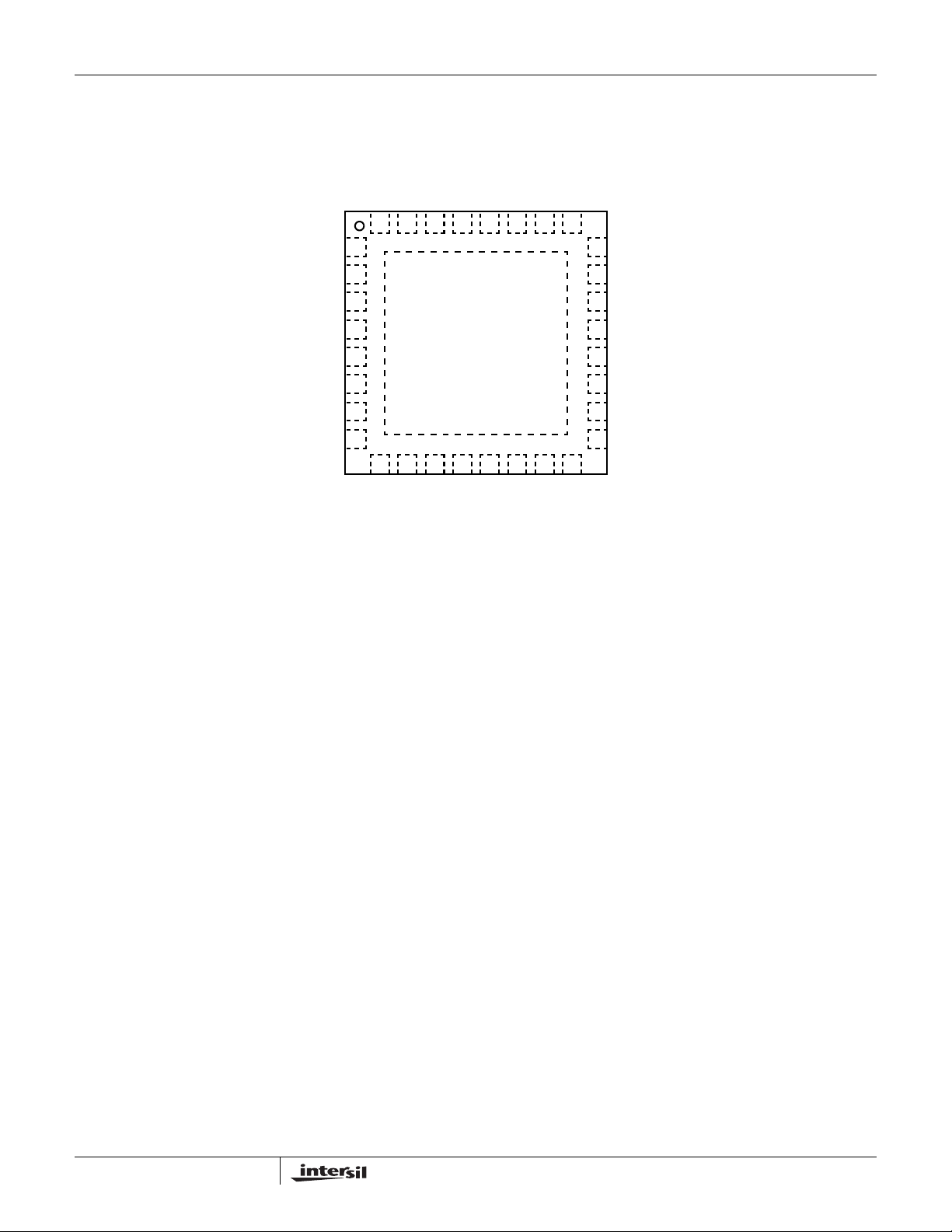
Pinout
www.BDTIC.com/Intersil
PGND
ISL6425
ISL6425 (32 LEAD 5x5 QFN)
TOP VIEW
NC
NC
NC
NC
NC
32 31 30 29 28 2 7 26 25
1
VCC
CPVOUT
CPSWOUT
24
NC
SGND
SEL18V
NC
BYPASS
PGND
GATE
2
3
4
5
6
7
8
9 10111213141516
FB
CS
COMP
NC
VSW
SDA
ADDR
NC
23
NC
22
NC
21
AGND
20
VOUT
19
DSQIN
18
TCAP
17
SCL CPSWIN
2
FN9176.1
February 8, 2005

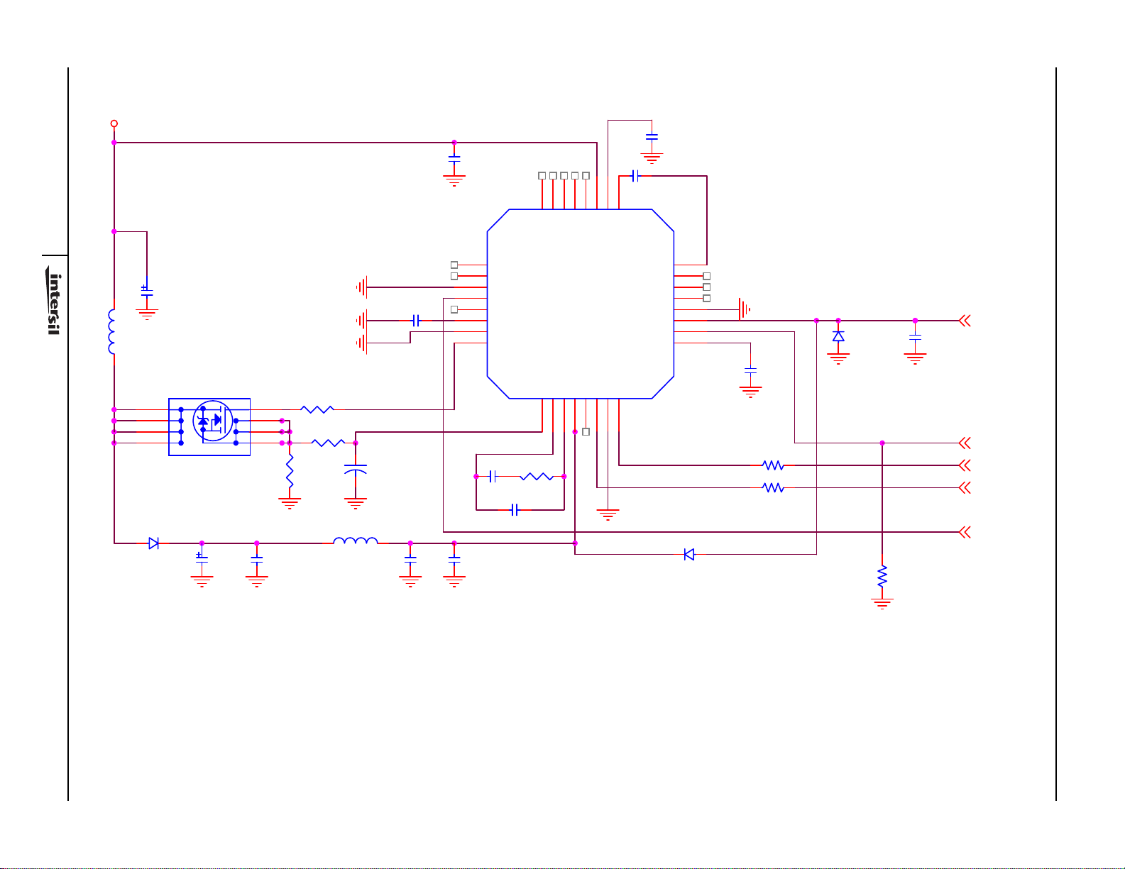
Typical Application Schematic
www.BDTIC.com/Intersil
VIN
3
2
L2
33uH
1
C6
56uF
0
6
7
8
D2
STPS2L40U
Q2
FDS6612A
C4
56uF
0
C17
C16
1uF
0
1
PGND
2
NC
C15
10uF
0
3
SGND
4
SEL18V
5
NC
6
BYP
7
PGND
8
GATE
C10 33p
0
0
C8 1uF
0
R6
C13
10uF
18
R5 100
R2
0.1
100pF
0
1 2
C2
0
L3 4.7uH
C14
10uF
45
3
2
1
00
32
NC
CS
9
R8 68KC9 1.5n
29
30
28
NC
NC31NC
NC
U1
ISL6425ER
COMP
VSW
NC
11FB10
12
13
27
26
VCC
CPVOUT
SDA14ADDR
15
0
25
CPSWIN
CPSWOUT
SCL
16
47nF
0
C18 1n
NC
NC
NC
AGND
VOUT
DSQIN
TCAP
D5 STPS2L40U
24
23
22
21
20
19
18
17
0
C20
0.22uF
0
R10 1k
R11 1k
D3
STPS2L40U
0
R13
100k
C22
0.1uF
0
VLNB1
ISL6425
DSQIN1
SCL
SDA
SEL18V1
0
February 8, 2005
FN9176.1

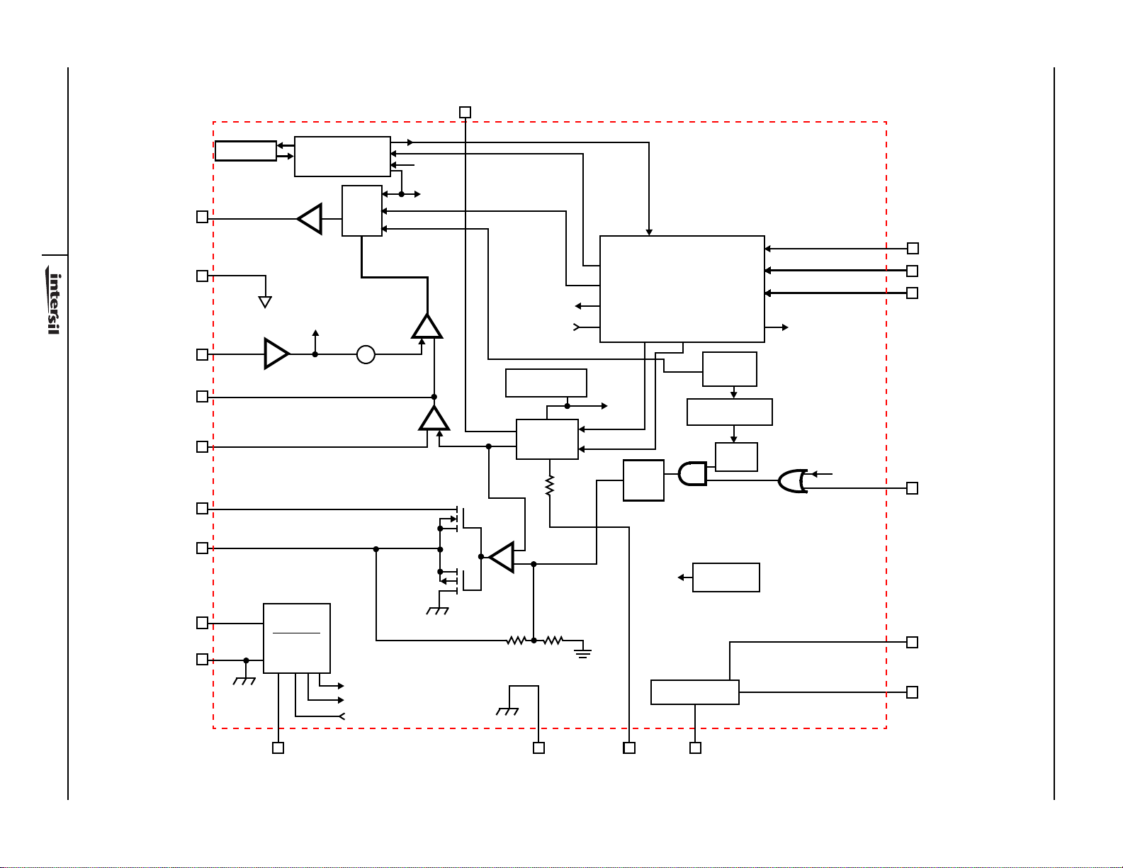
Block Diagram
www.BDTIC.com/Intersil
7
-
+
VREF
SEL18V
BAND GAP
RE F VO LTA GE
REF
VOLTAGE
ADJ
ISEL
EN
ENT
OTF
BGV
OLF
INTERFACE
LLC VSEL
TONE
INJ
CKT
I2C
OSC.
CLK
220kHz
÷ 10 AND
WAVE SHAP ING
22kHz
TONE
SDA
ADDR
SCL
DCL
ENT
SDA
ADDR
SCL
DSQIN
15
16
17
ISL6425
19
COUNTER
GATE
10
4
E PAD
PGND
CS
11
COMP
13
FB
12
VSW
14
OVERCURRENT
PROTECTION
LOGIC SCHEME 1
ILIM
CS
AMP
PWM
LOGIC
Q
S
∑
SLOPE
COMPENSATION
OLF
DCL
OC
CLK
+
VOUT
20
VCC
28
SGND
6
February 8, 2005
FN9176.1
ON CHIP
LINEAR
UVLO
POR
SOFT-START
BYPASS
9
INT 5V
SOFT-START
EN
+
-
AGND
OTF
TCAP
THERMAL
SHUTDOWN
CHARGE PUMP
CPSWOUT
251821
CPVOUT
CPSWIN
27
26
 Loading...