®
www.BDTIC.com/Intersil
ISL6423
Data Sheet
Single Output LNB Supply and Control
Voltage Regulator with I2C Interface for
Advanced Satellite Set-Top Box Designs
DiSEqC 2.0 Compatible
The ISL6423 is a highly integrated voltage regulator and
interface IC, specifically designed for supplying power and
control signals from advanced satellite set-top box (STB)
modules to the low noise blocks (LNBs) of single antenna
ports. The device consists of a current-mode boost PWM
and a low-noise linear regulator along with the circuitry
required for 22kHz tone generation, modulation and I
device interface. The device makes the total LNB supply
design simple, efficient and compact with low external
component count.
The current mode boost converter provides the linear
regulator with input voltage that is set to the final output
voltages, plus typically 0.8V to insure minimum power
dissipation across the linear regulator. This maintains
constant voltage drop across the linear pass element while
permitting adequate voltage range for tone injection.
The final regulated output voltage is available at output
terminals to support the operation of an antenna port for
single tuners. The outputs for each PWM can be controlled
in two ways, full control from I
bits or set the I
switch to higher range (i.e., 18.3V/19.3V) with the SELVT OP
pin. All the functions on this IC are controlled via the I
by writing 8 bits words onto the System Registers (SR). The
same register can be read back, and five I
the diagnostic status. Separate enable command sent on the
2
I
C bus provides for standby mode control for the PWM and
linear combination, disabling the output and forcing a shutdown
mode. The output channel is capable of providing 750mA of
continuous current. The overcurrent limit can be digitally
programmed to four levels.
The External modulation input EXTM can accept a
modulated DiSEqC command and transfer it symmetrically
to the output. Alternatively the EXTM pin can be used to
modulate the continuous internal tone.
The FLT
an over temperature fault condition is detected by the LNB
controller. The nature of the fault can be read of the I
registers.
2
C to the lower range (i.e., 13.3V/14.3V) and
pin serves as an interrupt for the processor when
2
C using the VTOP and VBOT
2
C bits will report
2
C
2
C bus
2
C
April 10, 2007
FN9191.1
Features
• Single Chip Power solution
- Operation for 1-Tuner/1-Dish Applications
- Integrated DC/DC Converter and I
• Switch-Mode Power Converter for Lowest Dissipation
- Boost PWM with > 92% Efficiency
- Selectable 13.3V or 18.3V Outputs
- Digital Cable Length Compensation (1V)
2
-I
C and Pin Controllable Output
• Output Back Bias Capability of 28V
2
C Compatible Interface for Remote Device Control
•I
• Registered Slave Address 0001 00XX
• 2.5V/3.3V/5V Logic Compatible
• External Pin to Toggle between V & H Polarization
• Built-In Tone Oscillator Factory Trimmed to 22kHz
- Facilitates DiSEqC (EUTELSAT) Encoding
- External Modulation Input
• Internal Over-Temperature Protection and Diagnostics
• Internal OV, UV, Overload and Overtemp Flags
(Visible on I
signal
•FLT
• LNB Short-Circuit Protection and Diagnostics
• QFN, HTSSOP Packages
• Pb-Free Plus Anneal Available (RoHS Compliant)
2
C)
2
C Interface
Applications
• LNB Power Supply and Control for Satellite Set-Top Box
Ordering Information
TEMP.
PART NUMBER
(Note)
ISL6423ERZ 6423ERZ -20 to +85 24 Ld 4x4 QFN L24.4x4D
ISL6423ERZ-T 6423ERZ -20 to +85 24 Ld 4x4 QFN
ISL6423EVEZ ISL6423EVEZ -20 to +85 28 Ld HTSSOP M28.173B
ISL6423EVEZ-T ISL6423EVEZ -20 to +85 28 Ld HTSSOP
NOTE: Inter sil Pb-free plus anneal products employ special Pb-free
material sets; molding compounds/die attach materials and 100% matte
tin plate termination finish, which are RoHS compliant and compatible
with both SnPb and Pb-free soldering operations. Intersil Pb-free
products are MSL classified at Pb-free peak reflow temperatures that
meet or exceed the Pb-free requirements of IPC/JEDEC J STD-020.
PART
MARKING
RANGE
(°C)
PACKAGE
(Pb-Free)
(T ape & Reel)
(T ape & Reel)
PKG.
DWG. #
L24.4x4D
M28.173B
1
CAUTION: These devices are sensitive to electrostatic discharge; follow proper IC Handling Procedures.
1-888-INTERSIL or 1-888-468-3774
| Intersil (and design) is a registered trademark of Intersil Americas Inc.
All other trademarks mentioned are the property of their respective owners.
Copyright Intersil Americas Inc. 2006, 2007. All Rights Reserved
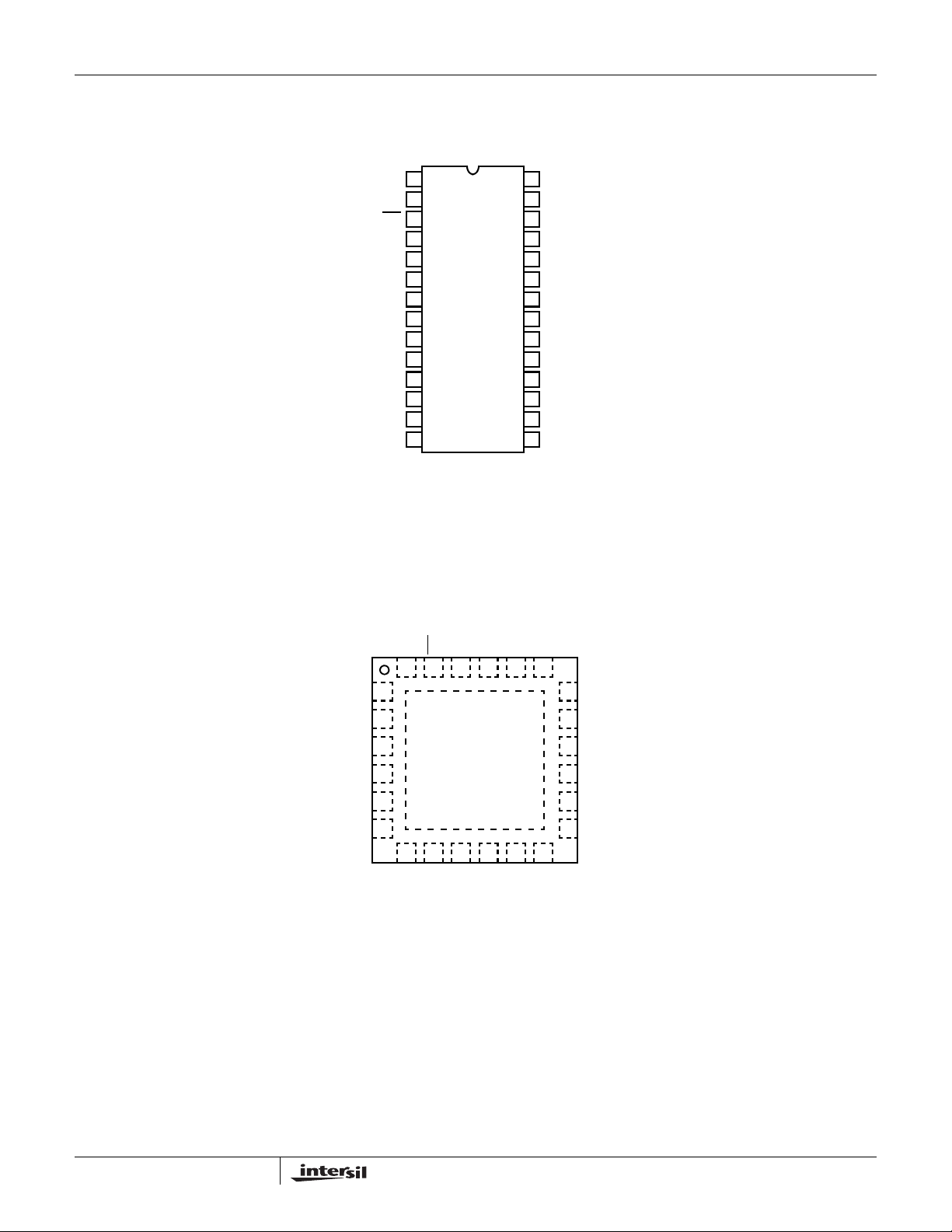
Pinouts
www.BDTIC.com/Intersil
VCC
NC
FLT
NC
SGND
TCAP
ADDR0
ADDR1
BYPASS
PGND
GATE
VSW
NC
CS
ISL6423
ISL6423 (HTSSOP)
TOP VIEW
1
2
3
4
5
6
7
8
9
10
11
12
13
14
28
CPSWIN
CPSWOUT
27
CPVOUT
26
EXTM
25
SDA
24
SCL
23
TDOUT
22
TDIN
21
20
VO
NC
19
NC
18
AGND
17
16
SELVTOP
TXT
15
SGND
TCAP
ADDR0
ADDR1
BYPASS
PGND
ISL6423 (QFN)
TOP VIEW
NC
FLT
VCC
CS
CPSWIN
TXT
24 23 22 21 20 19
1
2
3
4
5
6
789101112
GATE
VSW
CPSWOUT
SELVTOP
CPVOUT
18
17
16
15
14
13
AGND
EXTM
SDA
SCL
TDOUT
TDIN
VO
2
FN9191.1
April 10, 2007
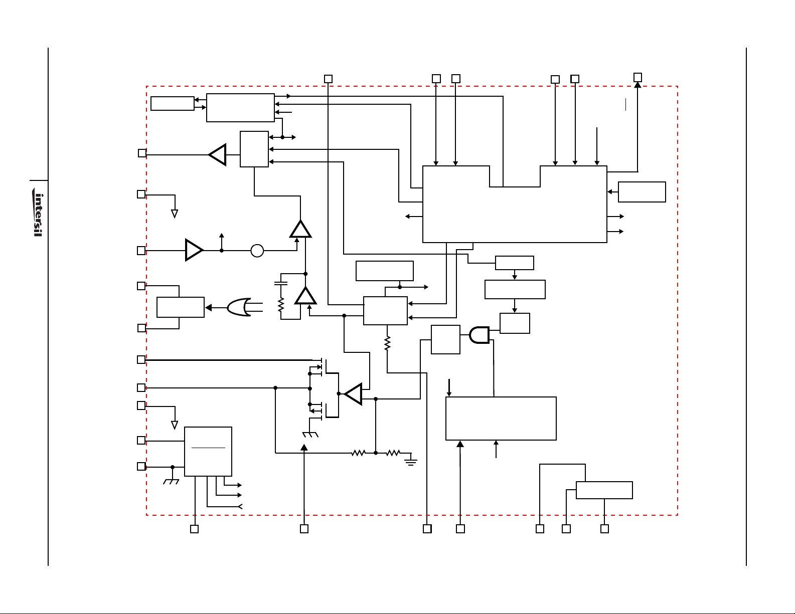
Block Diagram
www.BDTIC.com/Intersil
11
17
16
4
3
23
CLK1
OLF/BCF
DCL
OC1
+
-
-
+
VREF1
SCL
SDA
SELVTOP
SDA
SCL
BAND GAP
REF VOLTAGE
REF
VOLTAGE
ADJ1
ISELL&H
EN
ENT
VTOP
BGV
TONE
INJ
CKT
VBOT
CLK1
OLF/BCF
I2C
INTERFACE
OSC.
DIV &
WAVE SHAPING
INT
TONE
ADDR0
ADDR0
ADDR1
OUVF
OUVF
ADDR1
OTF
TTH
DCL
FLT
THERMAL
SHUTDOWN
ISL6423
COUNTER
GATE
7
3
PGND
6
CS
9
TDOUT
15
TONE
DECODER
TDIN
14
VSW
8
OVERCURRENT
PROTECTION
LOGIC SCHEME 1
ILIM1
CS
AMP
PWM
LOGIC
Q
S
∑
SLOPE
COMPENSATION
TXT
TTH
VO
13
AGND
12
VCC
22
SGND
1
April 10, 2007
FN9191.1
NOTE:
ON CHIP
LINEAR
UVLO
POR
SOFT-START
BYPASS
5
INT 5V
SOFT-START
EN1/EN2
TXT
10
+
-
1. Pinouts shown are for the QFN package.
TCAP
2
MSEL1
EXTM
18
EXT TONE CKT
ENT1
CPSWOUT
CPSWIN
20 21
CHARGE PUMP
CPVOUT
19
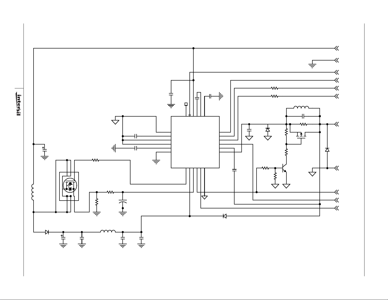
Typical Application Schematic QFN
www.BDTIC.com/Intersil
VIN
RTN
0
4
2
L5
15µH
1
C23
56µF
0
1234
5
6
TPC6002
Q2
R10
18
0
R8
0.1
0
R9
470
C21
100pF
0
C27
C26
0.22µF
1µF
C29
1n
23
VSW
8CS9
22
FLT
U2
C25 47n
19
20
21
VCC
CPSWIN
CPSWOUT
TXT10AGND
SELVTOP
11
12
CPVOUT
EXTM
SDA
SCL
TDOUT
TDIN
VO
D7
0
18
17
16
15
14
13
C16
10n
CMS06
C24
1µF
0
24
1
SGND
2
TCAP
3
ADDR0
4
ADDR1
5
BYPASS
6
PGND
0
SGND
ISL6423ER
GATE
7
C28
0.1µF
R11 100
R12
D6
CMS06
R13 4.7k
R22
47k
100
R23
10k
R24
4.7k
L4
220µH
1 2
C15
0.22µF
R7
NDS356AP
Q4
2N2222A
15
M6
FLT BAR
EXTM
SDA
SCL
VLNB
ISL6423
D8
1.5KE24
RTN
TXT
TDOUT
SELVTOP
D5
CMS06
April 10, 2007
FN9191.1
C22
56µF
0
C18
10µF
0
L6
4.7µH
1 2
C19
10µF
0
C20
10µF
0
NOTE : SDA and SCL require pull up to the required logic level.
ISL6423
www.BDTIC.com/Intersil
Absolute Maximum Ratings Thermal Information
Supply Voltage, VCC . . . . . . . . . . . . . . . . . . . . . . . . . . 8.0V to 18.0V
Logic Input Voltage Range
(SDA, SCL, ENT, DSQIN 1 and 2, SEL18V 1 and 2). .-0.5V to 7V
CAUTION: Stresses above those listed in “Absolute Maximum Ratings” may cause permanent damage to the device. This is a stress only rating and operation of the
device at these or any other conditions above those indicated in the operational sections of this specification is not implied.
NOTES:
2. θ
is measured in free air with the component mounted on a high effective thermal conductivity test board with “direct attach” features. See
JA
Tech Brief TB379.
3. For θ
4. The device junction temperature should be kept below +150°C. Thermal shut-down circuitry turns off the device if junction temperature exceeds
, the "case temp" location is the center of the exposed metal pad on the package underside.
JC
+150°C typically.
Thermal Resistance (Typical, Notes 2, 3) θJA (°C/W) θJC (°C/W)
QFN Package. . . . . . . . . . . . . . . . . . . . 38 4.5
TSSOP Package . . . . . . . . . . . . . . . . . 35 2.5
Maximum Junction Temperature (Note 4) . . . . . . . . . . . . . . .+150°C
Maximum Storage Temperature Range. . . . . . . . . .-40°C to +150°C
Operating Temperature Range . . . . . . . . . . . . . . . . .-20°C to +85°C
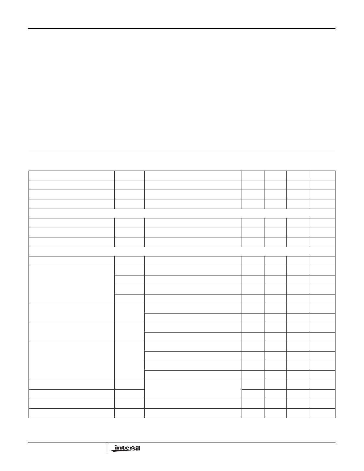
Electrical Specifications V
PARAMETER SYMBOL TEST CONDITIONS MIN TYP MAX UNITS
Operating Supply Voltage Range 81214 V
Standby Supply Current EN = L - 1.5 3.0 mA
Supply Current I
UNDERVOLTAGE LOCKOUT
Start Threshold 7.5 - 7.95 V
Stop Threshold 7.0 - 7.6 V
Start to Stop Hysteresis 350 400 500 mV
SOFT-START
COMP Rise Time (Note 5) (Note 5) - 8196 - Cycles
Output Voltage (Note 5) V
Line Regulation DV
Load Regulation DV
Dynamic Output Current Limiting I
Dynamic Overload Protection Off Time TOFF DCL = 0, Output Shorted (Note 8) - 900 - ms
Dynamic Overload Protection On Time TON - 20 - ms
Static Output Current Limiting I
Cable Fault CABF Threshold I
= 12V, TA = -20°C to +85°C, unless otherwise noted. Typical values are at TA = +25°C. EN = H, VTOP
CC
VBOT = L, ENT = L, DCL = L, Iout = 12mA, unless otherwise noted. See software description section for I
access to the system.
EN = VTOP = VBOT = ENT = H, No Load - 4.0 8.0 mA
(Refer to Table 1) 13.04 13.3 13.56 V
(Refer to Table 1) 14.02 14.3 14.58 V
(Refer to Table 1) 17.94 18.3 18.66 V
(Refer to Table 1) 19.00 19.3 19.68 V
VIN = 8V to 14V; VO = 13.3V - 4.0 40.0 mV
O1,
O2
O1,
O2
= 8V to 14V; VO = 18.3V - 4.0 60.0 mV
V
IN
IO = 0mA to 350mA - 50 80 mV
= 0mA to 750mA - 100 200 mV
I
O
DCL = 0, ISEL H = 0, ISEL L = 0 (Note 8) 275 305 345 mA
DCL = 0, ISEL H = 0, ISEL L = 1 (Note 8) 515 570 630 mA
DCL = 0, ISEL H = 1, ISEL L = 0 (Note 8) 635 705 775 mA
DCL = 0, ISEL H = 1, ISEL L = 1 (Note 8) 800 890 980 mA
DCL = 1 (Note 8) - 990 - mA
EN = 1, VO = 19V, No Tone 2 10 20 mA
V
V
V
DV
DV
IN
O1
O1
O1
O1
MAX
MAX
CAB
2
C
5
FN9191.1
April 10, 2007
 Loading...