

Page 1
®
www.BDTIC.com/Intersil
ISL6416
Data Sheet November 3, 2004
Triple Output, Low-Noise LDO Regulator
with Integrated Reset Circuit
The ISL6416 is an ultra low noise triple output LDO regulator
with microprocessor reset circuit and is optimized for
powering wireless chip sets. The IC accepts an input voltage
range of 3.0V to 3.6V and provides three regulated output
voltages: 1.8V (LDO1), 2.8V (LDO2), and another ultra-clean
2.8V (LDO3). On chip logic provides sequencing between
LDO1 and LDO2 for the BBP/MAC and the I/O supply
voltage outputs. LDO3 features ultra low noise that does not
exceed 30µV
integration makes the ISL6416 an ideal choice to power
many of today’s small form factor industry standard wireless
cards such as PCMCIA, mini-PCI and Cardbus-32.
The ISL6416 uses an internal PMOS transistor as the pass
device. The ISL6416 also integrates a reset function, which
eliminates the need for the additional reset IC required in
WLAN applications. The IC asserts a RESET
whenever the VIN supply voltage drops below a preset
threshold, keeping it asserted for at least 25ms after Vin has
risen above the reset threshold. FAULT indicates the loss of
regulation on LDO1.
(typical) to aid VCO stability. High
RMS
signal
Ordering Information
PART NUMBER
ISL6416IA -40 to +85 16 Ld QSOP M16.15A
ISL6416IAZ (Note 1) -40 to +85 16 Ld QSOP
NOTES:
1. Tape and Reel available. Add “-T” suffix for Tape and Reel
Packing Option.
2. Intersil Pb-free products employ special Pb-free material sets;
molding compounds/die attach materials and 100% matte tin
plate termination finish, which are RoHS compliant and
compatible with both SnPb and Pb-free soldering operations.
Intersil Pb-free products are MSL classified at Pb-free peak
reflow temperatures that meet or exceed the Pb-free
requirements of IPC/JEDEC J STD-020C.
TEMP.
RANGE (°C) PACKAGE
(Pb-free)
PKG.
DWG. #
M16.15A
FN9193.0
Features
• Three LDOs and a RESET circuit
• High Output Current
- LDO1, 1.8V. . . . . . . . . . . . . . . . . . . . . . . . . . . . . 330mA
- LDO2, 2.8V. . . . . . . . . . . . . . . . . . . . . . . . . . . . . 225mA
- LDO3, 2.8V. . . . . . . . . . . . . . . . . . . . . . . . . . . . . 125mA
• Low Output Voltage Noise
- <30µV
• Stable with Small Ceramic Output Capacitors
• Extensive Protection and Monitoring Features
- Overcurrent protection
- Short circuit protection
- Thermal shutdown
- FAULT indicator
• Logic-Controlled Shutdown Pin
• Integrated Microprocessor Reset Circuit
- Programmable Reset Delay
• Proven Reference Design for a Total WLAN System
Solution
• Pb-Free Available (RoHS Compliant)
(typical) for LDO3 (VCO Supply)
RMS
Applications
•WLAN Cards
- PCMCIA, Cardbus32, MiniPCI Cards
- Compact Flash Cards
• Hand-Held Instruments
1
CAUTION: These devices are sensitive to electrostatic discharge; follow proper IC Handling Procedures.
1-888-INTERSIL or 321-724-7143
| Intersil (and design) is a registered trademark of Intersil Americas Inc.
Copyright © Intersil Americas Inc. 2004. All Rights Reserved. All Rights Reserved.
All other trademarks mentioned are the property of their respective owners.
Page 2
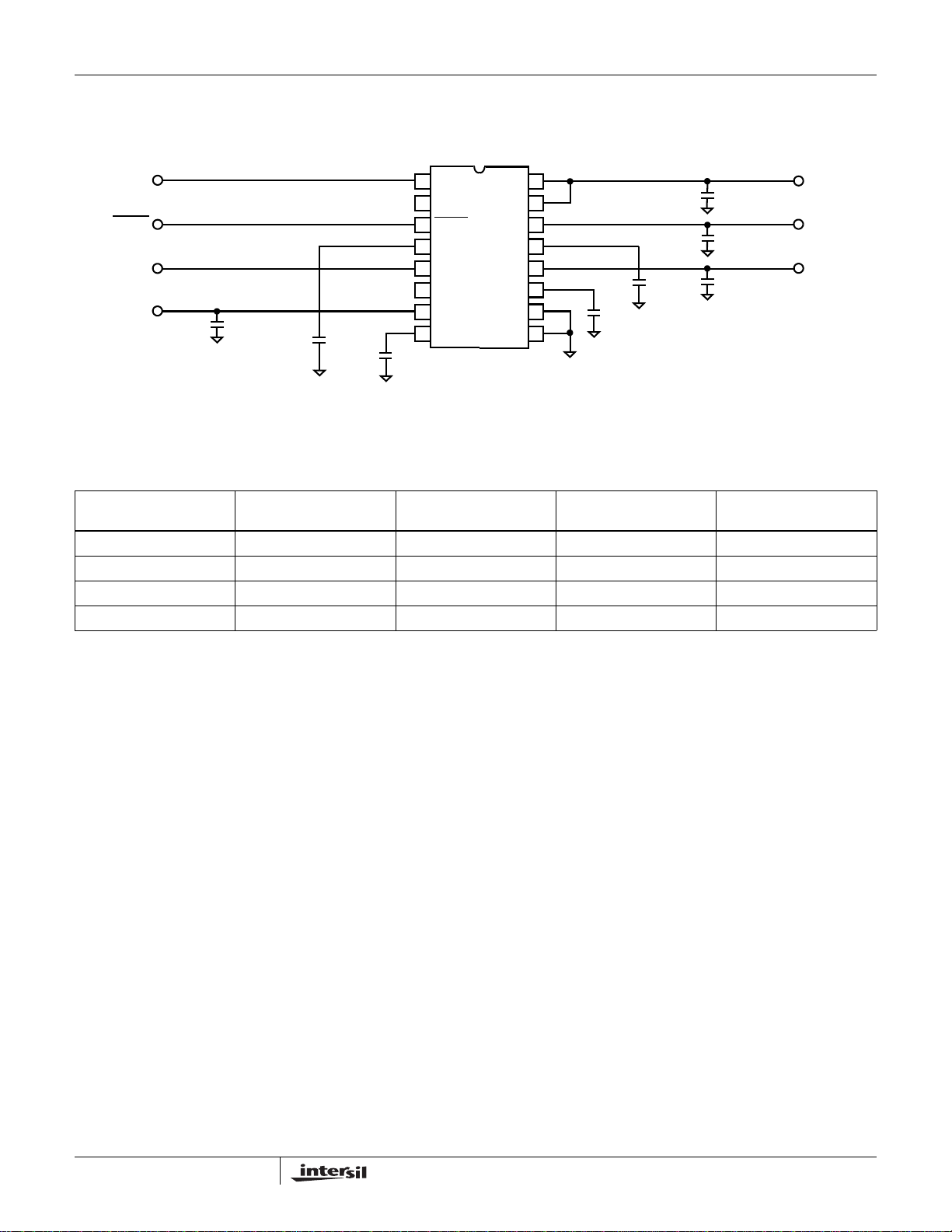
Pinout and Typical Application Schematic
www.BDTIC.com/Intersil
ISL6416 (QSOP)
FAULT
RESET
SHDN
VOUT3
+2.8V
C4
10µF
C8
0.01µF
1
2
3
4
5
6
7
8
C7
0.033µF
Typical Bill Of Materials
ISL6416
TOP VIEW
FAU LT
NC
RESET
CT
SHDN
NC
VOUT3
CC3
VIN
VIN
VOUT1
CC1
VOUT2
CC2
GND
GND
V
16
15
14
13
12
11
10
9
0.033µF
C6
C5
0.033µF
C1
10µF
C2
10µF
C3
10µF
IN
+3.3V
VOUT1
+1.8V
VOUT2
+2.8V
REFERENCE
DESIGNATOR VALUE PACKAGE MANUFACTURER
MANUFACTURER’S
PART NUMBER
C1, C2, C3, C4 10µF, X7R 1206 TDK C3216X7R1A106M
C5, C6, C7 0.033µF, X7R 0603 TDK/ANY C1608X7R1A333K
C8 0.01µF, X7R 0603 TDK/ANY C1608X7R1A103K
U1 ISL6416IA QSOP16 Intersil ISL6416IA
2
FN9193.0
November 3, 2004
Page 3

ISL6416
www.BDTIC.com/Intersil
Shrink Small Outline Plastic Packages (SSOP)
Quarter Size Outline Plastic Packages (QSOP)
N
INDEX
AREA
123
-A-
E
-B-
SEATING PLANE
D
A
-C-
0.25(0.010) B
H
α
e
B
0.17(0.007) C AMB
NOTES:
1. Symbols are defined in the “MO Series Symbol List” in Section
2.2 of Publication Number 95.
2. Dimensioning and tolerancing per ANSI Y14.5M-1982.
3. Dimension “D” does not include mold flash, protrusions or gate
burrs. Mold flash, protrusion and gate burrs shall not exceed
0.15mm (0.006 inch) per side.
4. Dimension “E” does not include interlead flash or protrusions.
Interlead flash and protrusions shall not exceed 0.25mm (0.010
inch) per side.
5. The chamfer on the body is optional. If it is not present, a visual
index feature must be located within the crosshatched area.
6. “L” is the length of terminal for soldering to a substrate.
7. “N” is the number of terminal positions.
8. Terminal numbers are shown for reference only.
9. Dimension “B” does not include dambar protrusion. Allowable
dambar protrusion shall be 0.10mm (0.004 inch) total in excess
of “B” dimension at maximum material condition.
10. Controlling dimension: INCHES. Converted millimeter dimensions are not necessarily exact.
M
A1
0.10(0.004)
S
GAUGE
PLANE
A2
M
0.25
0.010
h x 45°
M
M16.15A
16 LEAD SHRINK SMALL OUTLINE PLASTIC PACKAGE
(0.150” WIDE BODY)
INCHES MILLIMETERS
SYMBOL
A 0.061 0.068 1.55 1.73 -
A1 0.004 0.0098 0.102 0.249 -
L
C
A2 0.055 0.061 1.40 1.55 -
B 0.008 0.012 0.20 0.31 9
C 0.0075 0.0098 0.191 0.249 -
D 0.189 0.196 4.80 4.98 3
E 0.150 0.157 3.81 3.99 4
e 0.025 BSC 0.635 BSC -
H 0.230 0.244 5.84 6.20 -
h 0.010 0.016 0.25 0.41 5
L 0.016 0.035 0.41 0.89 6
N16 167
α
0° 8° 0° 8° -
NOTESMIN MAX MIN MAX
Rev. 2 6/04
All Intersil U.S. products are manufactured, assembled and tested utilizing ISO9000 quality systems.
Intersil Corporation’s quality certifications can be viewed at www.intersil.com/design/quality
Intersil products are sold by description only. Intersil Corporation reserves the right to make changes in circuit design, software and/or specifications at any time without
notice. Accordingly, the reader is cautioned to verify that data sheets are current before placing orders. Information furnished by Intersil is believed to be accurate and
reliable. However, no responsibility is assumed by Intersil or its subsidiaries for its use; nor for any infringements of patents or other rights of third parties which may result
from its use. No license is granted by implication or otherwise under any patent or patent rights of Intersil or its subsidiaries.
For information regarding Intersil Corporation and its products, see www.intersil.com
10
FN9193.0
November 3, 2004
 Loading...