

®
www.BDTIC.com/Intersil
O
F
D
E
D
N
E
M
T
O
N
IB
Data Sheet August 2004
S
S
O
P
D
O
R
P
M
O
C
E
R
B
U
S
E
L
I
:
T
C
U
W
E
N
R
T
U
T
I
T
S
2
1
4
6
L
S
D
E
G
I
S
E
S
N
ISL6414
FN9128.1
Triple Output, Low-Noise LDO Regulator
with Integrated Reset Circuit
The ISL6414 is an ultra low noise triple output LDO regulator
with microprocessor reset circuit and is optimized for
powering wireless chip sets. The IC accepts an input voltage
range of 3.0V to 3.6V and provides three regulated output
voltages: 1.8V (LDO1), 2.84V (LDO2), and another ultra
clean 2.84V (LDO3). On chip logic provides sequencing
between LDO1 and LDO2 for BBP/MAC and I/O supply
voltage outputs. LDO3 features ultra low noise that does not
typically exceed 30µV RMS to aid VCO stability. High
integration and the thin Quad Flat No-lead (QFN) package
makes ISL6414 an ideal choice to power many of today’s
small form factor industry standard wireless cards, such as
PCMCIA, mini-PCI and Cardbus-32.
The ISL6414 uses an internal PMOS transistor as the pass
device. The SHDN pin controls LDO1 and LDO2 outputs
whereas SHDN3 controls LDO3 output. Internal voltage
sequencing insures that LDO1 output (1.8V supply) is
always stabilized before LDO2 is turned on. When powering
down, power to the LDO2 is removed before the LDO1
output goes off. The ISL6414 also integrates RESET
function, which eliminates the need for additional RESET IC
required in WLAN applications. The IC asserts a RESET
signal whenever the V
threshold, keeping it asserted for at least 25ms after V
risen above the reset threshold. An output fault detection
circuit indicates loss of regulation on LDO1. Other features
include an overcurrent protection, thermal shutdown and
reverse battery protection.
supply voltage drops below a preset
IN
IN
has
Ordering Information
TEMP.
PART NUMBER
ISL6414IR -40 to +85 16 Ld QFN L16.4x4
ISL6414IR-T5K 16 Ld QFN Tape and Reel L16.4x4
ISL6414IR-TK 16 Ld QFN Tape and Reel L16.4x4
ISL6414IRZ (Note) -40 to +85 16 Ld QFN
ISL6414IRZ-TK
(Note)
NOTE: Intersil Pb-free plus anneal products employ special Pb-free
material sets; molding compounds/die attach materials and 100%
matte tin plate termination finish, which are RoHS compliant and
compatible with both SnPb and Pb-free soldering operations. Intersil
Pb-free products are MSL classified at Pb-free peak reflow
temperatures that meet or exceed the Pb-free requirements of
IPC/JEDEC J STD-020.
RANGE (°C) PACKAGE
(Pb-free)
16 Ld QFN Tape and Reel
(Pb-free)
PKG.
DWG. #
L16.4x4
L16.4x4
Features
• Small DC/DC Converter Size
- Three LDOs and RESET Circuitry in a Low-Profile
4x4mm QFN Package
• High Output Current
- LDO1, 1.8V. . . . . . . . . . . . . . . . . . . . . . . . . . . . . 500mA
- LDO2, 2.84V. . . . . . . . . . . . . . . . . . . . . . . . . . . . 300mA
- LDO3, 2.84V. . . . . . . . . . . . . . . . . . . . . . . . . . . . 200mA
• Ultra-Low Dropout Voltage
- LDO2, 2.84V. . . . . . . . . . . . . . . 125mV (typ.) at 300mA
- LDO3, 2.84V. . . . . . . . . . . . . . . 100mV (typ.) at 200mA
• Ultra-Low Output Voltage Noise
-<30µV
• Stable with Smaller Ceramic Output Capacitors
• Voltage Sequencing for BBP/MAC and Analog Supplies
• Extensive Protection and Monitoring Features
- Overcurrent and short circuit protection
- Thermal shutdown
- Reverse battery protection
- FAULT indicator
• Logic-Controlled Dual Shutdown Pins
• Integrated Microprocessor Reset Circuit
- Programmable Reset Delay
- Complimentary Reset Outputs
• Proven Reference Design for Total WLAN System
Solution
• QFN Package Option
- Compliant to JEDEC PUB95 MO-220 QFN - Quad Flat
No Leads - Product Outline
- Near Chip-Scale Package Footprint Improves PCB
Efficiency and Is Thinner in Profile
• Pb-Free Plus Anneal Available (RoHS Compliant)
(typ.) for LDO3 (VCO Supply)
RMS
Applications
• PRISM® 3, PRISM GT™, and PRISM WWR Chipsets
•WLAN Cards
- PCMCIA, Cardbus32, MiniPCI Cards
- Compact Flash Cards
• Hand-Held Instruments
1
CAUTION: These devices are sensitive to electrostatic discharge; follow proper IC Handling Procedures.
1-888-INTERSIL or 1-888-468-3774
| Intersil (and design) is a registered trademark of Intersil Americas Inc.
All other trademarks mentioned are the property of their respective owners.
Copyright © Intersil Americas Inc. 2003-2005. All Rights Reserved.
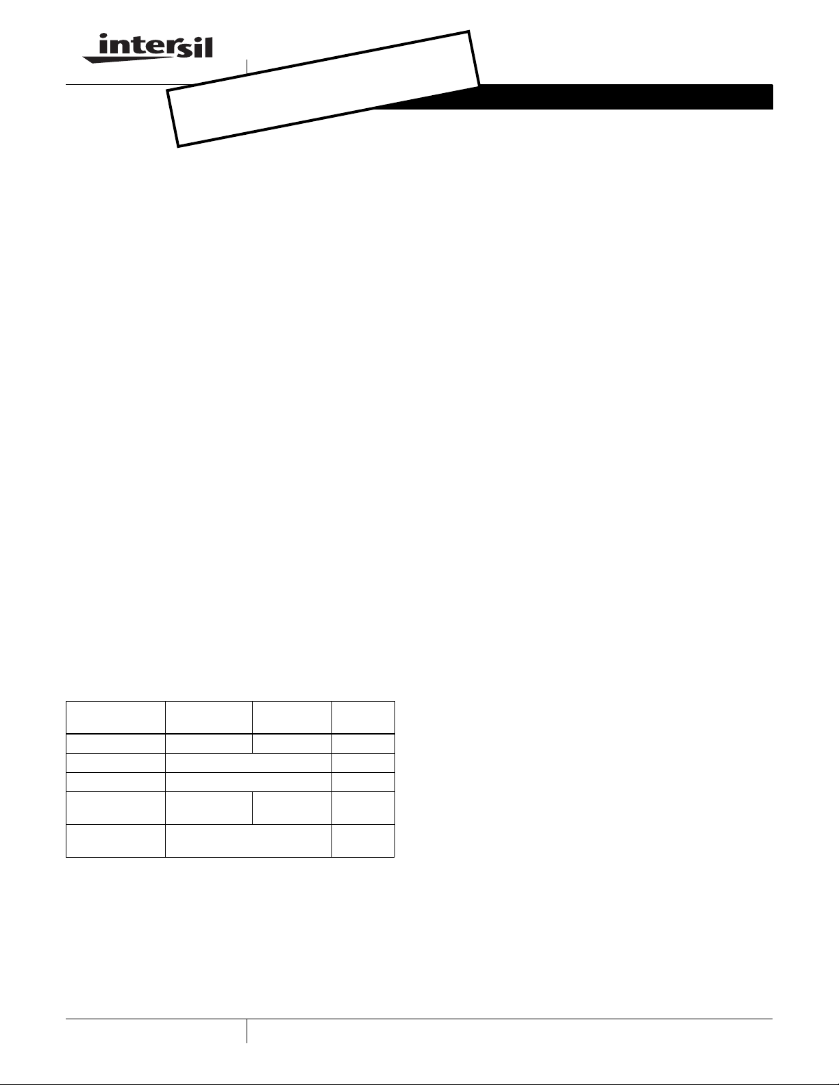
Pinout
www.BDTIC.com/Intersil
ISL6414 (QFN)
TOP VIEW
RESET
FAULT
VIN
1516 14 13
ISL6414
VIN
RESET
CT
SHDN
SHDN3
1
2
3
4
6578
CC3
OUT3
GND3
12
11
10
9
GND
Typical Application Schematic
+3.3V
V
IN
+
C8
3.3µF
1
RESET
2
CT
3
4
SHDN
SHDN3
V
OUT3
+2.84V
C7
0.01µF
C5
3.3µF
OUT1
CC1
OUT2
CC2
16
RESET
ISL6414
CC3
OUT3
5
6
14
15
FAULT
GND3
7
E
C6
0.033µF
VIN
GND
8
13
VIN
OUT1
OUT2
CC1
CC2
E
+1.8V
V
OUT1
12
11
10
9
C4
0.033µF
C3
0.033µF
C2
3.3µF
C1
3.3µF
+2.84V
V
OUT2
2
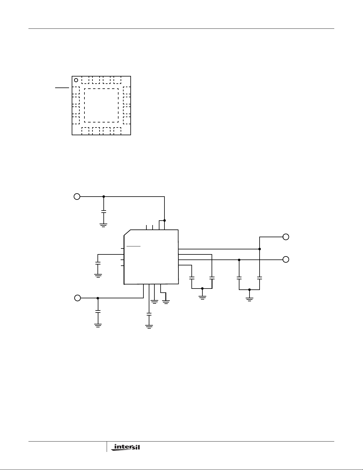
Functional Block Diagram
www.BDTIC.com/Intersil
VIN
15
FAU LT
BAND
GAP
REF.
1.2V
THERMAL
SHUT
DOWN
150°C
ISL6414
WINDOW
COMP
Gm
Gm
13
VIN
14
VIN
+
-
LDO1
+
-
LDO2
OUT1
OUT2
12
11CC1
10
VIN
CONTROL
LOGIC
3
SHDN
4
SHDN3
ENABLES
2
CT
16
RESET
1
RESET
8
GND
RESET
POR
POR
Gm
+
-
LDO3
CC2
OUT3 5
CC3
GND3
9
6
7
3
ISL6414
www.BDTIC.com/Intersil
Absolute Maximum Ratings (Note 1) Thermal Information
VIN, SHDN/SHDN3 to GND/GND3 . . . . . . . . . . . . . . . -7.0V to 7.0V
SET, CC, FAULT to GND/GND3 . . . . . . . . . . . . . . . . . -0.3V to 7.0V
Output Current (Continuous)
LDO1 . . . . . . . . . . . . . . . . . . . . . . . . . . . . . . . . . . . . . . . . 500mA
LDO2 . . . . . . . . . . . . . . . . . . . . . . . . . . . . . . . . . . . . . . . . 300mA
LDO3 . . . . . . . . . . . . . . . . . . . . . . . . . . . . . . . . . . . . . . . . 200mA
ESD Classification . . . . . . . . . . . . . . . . . . . . . . . . . . . . . . . . . Class 1
CAUTION: Stresses above those listed in “Absolute Maximum Ratings” may cause permanent damage to the device. This is a stress only rating and operation of the
device at these or any other conditions above those indicated in the operational sections of this specification is not implied.
NOTES:
1. All voltages are with respect to GND.
is measured in free air with the component mounted on a high effective thermal conductivity test board with “direct attach” features. See
2. θ
JA
Tech Brief TB379.
3. For θ
, the “case temp” location is the center of the exposed metal pad on the package underside. See Tech Brief TB379.
JC
Thermal Resistance (Typical Notes 2, 3) θ
QFN Package. . . . . . . . . . . . . . . . . . . . 46 8.0
Maximum Junction Temperature (Plastic Package) . -55°C to 150°C
Maximum Storage Temperature Range. . . . . . . . . . . -65°C to 150°C
Maximum Lead Temperature (Soldering 10s) . . . . . . . . . . . . . 300°C
Operating Temperature Range . . . . . . . . . . . . . . . . . . -40°C to 85°C
(°C/W) θJC (°C/W)
JA
Electrical Specifications V
PARAMETER TEST CONDITIONS MIN TYP MAX UNITS
GENERAL SPECIFICATIONS
V
Voltage Range (Note 7) 3.0 3.3 3.6 V
IN
Operating Supply Current I
Shutdown Supply Current SHDN/SHDN3 = GND - 5 15 µA
SHDN/SHDN3 Input Threshold V
FAULT Output Low Voltage I
Thermal Shutdown Temperature (Note 6) 145 150 160 °C
Thermal Shutdown Hysteresis - 20 - °C
Start-up Time C
Input Undervoltage Lockout (Note 6) Rising 75mV Hysteresis 2.2 2.45 2.65 V
LDO1 SPECIFICATIONS
Output Voltage (V
Output Voltage Accuracy I
Line Regulation V
Load Regulation I
Maximum Output Current (I
Output Current Limit (Note 6) 0.55 0.6 1.0 A
Output Voltage Noise 10Hz < f < 100kHz, C
LDO2 SPECIFICATIONS
Output Voltage (V
Output Voltage Accuracy I
Maximum Output Current (I
Output Current Limit (Note 6) 330 770 - mA
Dropout Voltage (Note 4) I
Line Regulation V
Load Regulation I
) -1.8- V
OUT1
OUT1
) -2.84- V
OUT2
OUT2
= +3.3V, Compensation Capacitor = 33nF, TA = 25°C, Unless Otherwise Noted.
IN
= 0mA - 600 850 µA
OUT
, VIN = 3V to 3.6V 2.0 - - V
IH
V
, VIN = 3V to 3.6V - - 0.4 V
IL
= 2mA - - 0.25 V
SINK
= 10µF, V
OUT
value
= 10mA -1.5 - 1.5 %
OUT
= 3.0V to 3.6V, I
IN
= 10mA to 500mA -1.5 - 1.5 %
OUT
) (Note 6) 500 - - mA
= 50mA
I
OUT
= 10mA -1.5 - 1.5 %
OUT
) (Note 6) VIN = 3.6V 300 - - mA
= 300mA - 125 220 mV
OUT
= 3.0V to 3.6V, I
IN
= 10mA to 300mA - 0.2 1.0 %
OUT
= 90% of final
OUT
OUT
OUT
OUT
- 120 - µs
= 10mA -0.15 0.0 0.15 %/V
= 4.7µF,
= 10mA -0.15 0.0 0.15 %/V
-115-µV
RMS
4

ISL6414
www.BDTIC.com/Intersil
Electrical Specifications V
= +3.3V, Compensation Capacitor = 33nF, TA = 25°C, Unless Otherwise Noted. (Continued)
IN
PARAMETER TEST CONDITIONS MIN TYP MAX UNITS
Output Voltage Noise 10Hz < f < 100kHz, I
C
= 2.2µF-65-µV
OUT
C
= 10µF-60-µV
OUT
OUT
= 10mA
RMS
RMS
LDO3 SPECIFICATIONS
Output Voltage (V
Output Voltage Accuracy I
Maximum Output Current (I
) -2.84- V
OUT3
= 10mA -1.5 - 1.5 %
OUT
) (Note 6) VIN = 3.6V 200 - - mA
OUT3
Output Current Limit (Note 6) 250 400 - mA
Dropout Voltage (Note 4) I
Line Regulation V
Load Regulation I
Output Voltage Noise 10Hz < f < 100kHz, I
= 200mA - 100 200 mV
OUT
= 3.0V to 3.6V, I
IN
= 10mA to 200mA - 0.2 1.0 %
OUT
= 2.2µF-30-µV
C
OUT
C
= 10µF-20-µV
OUT
= 10mA -0.15 0.0 0.15 %/V
OUT
= 10mA
OUT
RMS
RMS
RESET BLOCK SPECIFICATIONS
RESET Threshold 2.564 2.630 2.696 V
RESET Threshold Hysteresis (Note 6) 6.3 - - mV
V
to RESET Delay VCC = VTH to VTH - 100mV - 20 - µs
IN
RESET/RESET
Active Timeout Period (Notes 5,6) 25 - - ms
FAULT
Rising Threshold % of VOUT 5.0 5.5 6.0 %
Falling Threshold % of VOUT -5.0 -5.5 -5.0 %
NOTES:
4. Specifications at -40°C are guaranteed by design/characterization, not production tested.
5. The dropout voltage is defines as V
- V
OUT,
when V
IN
is 50mV below the value of V
OUT
OUT
for VIN = V
OUT
+ 0.5V.
6. The RESET time is linear with CT at a slope of 2.5ms/nF. Thus, at 10nF (0.01µF) the RESET time is 25ms; at 100nF (0.1µF) the RESET time
would be 250ms.
7. Guaranteed by design, not production tested.
8. LDO1 is guaranteed by design to be within regulation at 2.7V minimum input voltage.
Typical Performance Curves
0.140
0.120
0.100
0.080
(V)
D
V
0.060
0.040
0.020
0.000
0.00 0.05 0.10 0.15 0.20 0.25 0.30
I
(Amps)
O
FIGURE 1. LD02 DROPOUT VOLTAGE FIGURE 2. LD03 DROPOUT VOLTAGE
5
0.100
0.090
0.080
0.070
0.060
(V)
D
0.050
V
0.040
0.030
0.020
0.010
0.000
0.00 0.05 0.10 0.15
(Amps)
I
O
0.30

Typical Performance Curves (Continued)
www.BDTIC.com/Intersil
V
= 1.8V
20
0
OUTPUT
VO LTAGE ( mV)
4
OUT
LOAD = 50mA
ISL6414
V
= 2.84V
20
0
OUTPUT
VOLTAGE (mV)
4
OUT
LOAD = 50mA
3
INPUT
VOLTAGE (V)
TIME (1ms/DIV)
FIGURE 3. LINE TRANSIENT RESPONSE (V
V
20
0
OUTPUT
VOLTAGE (mV)
4
3
INPUT
VOLTAGE (V)
TIME (1ms/DIV)
OUT
LOAD = 50mA
FIGURE 5. LINE TRANSIENT RESPONSE (V
3
INPUT
VOLTAGE (V)
TIME (1ms/DIV)
1) FIGURE 4. LINE TRANSIENT RESPONSE (V
OUT
= 2.84V
3) FIGURE 6. LOAD TRANSIENT RESPONSE (V
OUT
10
5
0
DEVIATION (mV)
OUTPUT VOLTAGE
100
LOAD
0
CURRENT (mA)
TIME (2ms/DIV)
V
V
OUT
= 3.3V
IN
OUT
= 1.8V
OUT
2)
1)
V
= 2.84V
10
5
0
DEVIATION (mV)
OU TPU T VOLTA GE
100
LOAD
0
CURRENT (mA)
TIME (2ms/DIV)
FIGURE 7. LOAD TRANSIENT RESPONSE (V
V
OUT
= 3.3V
IN
10
5
0
DEVIATION (mV)
OU TPU T VOLTA GE
100
LOAD
0
CURRENT (mA)
2) FIGURE 8. LOAD TRANSIENT RESPONSE (V
OUT
6
TIME (2ms/DIV)
V
V
OUT
= 3.3V
IN
= 2.84V
OUT
3)

Typical Performance Curves (Continued)
www.BDTIC.com/Intersil
ISL6414
1.2
1.1
1
0.9
LOAD REGULATION (%)
0.8
-40 -15 10 35 60 85
TEMPERATURE (°C)
1.6
1.5
1.4
1.3
1.2
LOAD REGULATION (%)
1.1
1
-40 -15 10 35 60 85
TEMPERATURE (°C)
FIGURE 9. LD01 LOAD REGULATION vs TEMPERATURE FIGURE 10. LD02 LOAD REGULATION vs TEMPERATURE
1.4
1.3
1.2
1.1
1
LOAD REGULATION (%)
0.9
0.8
-40 -15 10 35 60 85
TEMPERATURE (°C)
0.04
0.03
0.02
0.01
0
-0.01
-0.02
-0.03
LINE REGULATION (%/V)
-0.04
-0.05
-40 -15 10 35 60 85
TEMPERATURE (°C)
FIGURE 11. LD03 LOAD REGULATION vs TEMPERATURE FIGURE 12. LD01 LINE REGULATION vs TEMPERATURE
0
-0.01
-0.02
-0.03
-0.04
LINE REGULATION (%/V)
-0.05
-0.06
-40 -15 10 35 60 85
TEMPERATURE (°C)
0
-0.002
-0.004
-0.006
-0.008
-0.001
-0.012
LINE REGULATION (%/V)
-0.014
-0.016
-40 -15 10 35 60 85
TEMPERATURE (°C)
FIGURE 13. LD02 LINE REGULATION vs TEMPERATURE FIGURE 14. LD03 LINE REGULATION vs TEMPERATURE
7

Typical Performance Curves (Continued)
www.BDTIC.com/Intersil
ISL6414
8.3
8.25
8.2
8.15
8.1
8.05
OPERATING CURRENT (µA)
8
-40 -15 10 35 60 85
TEMPERATURE (°C)
720
710
700
690
680
670
660
650
640
630
OPERATING CURRENT (µA)
620
610
-40 -15 10 35 60 85
TEMPERATURE (°C)
FIGURE 15. SHUTDOWN CURRENT vs TEMPERATURE FIGURE 16. OPERATING CURRENT vs TEMPERATURE
180
160
140
120
100
80
60
40
DROPOUT VOLTAGE (mV)
20
0
-40 -15 10 35 60 85
TEMPERATURE (°C)
100
90
80
70
(mV)
60
50
40
DROPOUT
30
20
10
0
-40 -10 25 85
TEMPERATURE (°C)
FIGURE 17. LD02 DROPOUT VOLTAGE vs TEMPERATURE FIGURE 18. LD03 DROPOUT VOLTAGE vs TEMPERATURE
0
-10
-20
-30
-40
PSRR (dB)
-50
VOLTAGE (V)
TIME (µs)
FIGURE 19. SHUTDOWN vs RESET and FAULT
-60
-70
-80
0.01 0.1 1 10 100 1000
FREQUENCY (kHz)
FIGURE 20. POWER SUPPLY REJECTION RATIO vs
FREQUENCY
8

ISL6414
www.BDTIC.com/Intersil
Pin Descriptions
OUT1 - This pin is the output for LDO1. Bypass with a
minimum of 2.2µF, low ESR capacitor to GND for stable
operation.
V
- Supply input pins. Connect to input power source.
IN
Bypass with 2.2µF capacitor to GND. Both V
tied together on the PC board, close to the IC.
GND - Ground pin for LDO1 and LDO2.
CC1 - Compensation Capacitor for LDO1. Connect a
0.033µF capacitor from CC1 to GND.
SHDN - Shutdown input for LDO1 and LDO2. Connect to IN
for normal operation. Drive SHDN pin LOW to turn off LDO1
and LDO2.
OUT2 - This pin is the output for LDO2. Bypass with a
minimum of 2.2µF, low ESR capacitor to GND for stable
operation.
CT - Timing pin for the RESET circuit pulse width.
CC2 - Compensation capacitor for LDO2. Connect a
0.033µF capacitor from CC2 to GND.
OUT3 - This pin is output for LDO3. Bypass with a minimum
of 2.2µF, low ESR capacitor to GND3 for stable operation.
pins must be
IN
Functional Description
The ISL6414 is a 3-in-1 multi-output, low dropout, regulator
designed for wireless chipset power applications. It supplies
three fixed output voltages 1.8V, 2.84V and 2.84V. The 1.8V
output from LDO1 remains active down to a V
(min.), ensuring proper BBP/MAC operation. Each LDO
consists of a 1.2V reference, error amplifier, MOSFET driver,
P-Channel pass transistor, dual-mode comparator and
internal feedback voltage divider.
The 1.2V band gap reference is connected to the error
amplifier’s inverting input. The error amplifier compares this
reference to the selected feedback voltage and amplifies the
difference. The MOSFET driver reads the error signal and
applies the appropriate drive to the P-Channel pass
transistor. If the feedback voltage is lower then the reference
voltage, the pass transistor gate is pulled lower, allowing
more current to pass and increasing the output voltage. If the
feedback voltage is higher then the reference voltage, the
pass transistor gate is driven higher, allowing less current to
pass to the output. The output voltage is fed back through an
internal resistor divider connected to OUT1/2/3 pins.
Additional blocks include an output overcurrent protection,
reverse battery protection, thermal sensor, fault detector,
RESET function and shutdown logic.
= 2.7V
IN
GND3 - Ground pin for LDO3.
CC3 - Compensation capacitor for LDO3. Connect a
0.033µF capacitor from CC3 to GND3.
SHDN3 - Shutdown input for LDO3. Connect to V
normal operation. Drive SHDN3 pin LOW to turn off LDO3.
FAULT - This is the power good indicator for LDO1. When
the 1.8V output is out of regulation (>±5%, typ.), this pin
goes LOW. This pin also goes LOW during thermal
shutdown and any overcurrent event on LDO1. Connect this
pin to GND, if unused. This pin remains HIGH in the
shutdown mode, as controlled by the SHDN pin (refer to
Figure 19).
RESET
- This pin is the active-LOW output of the push-pull
output stage of the integrated reset supervisory circuit. The
reset circuit monitors V
pin, if V
output remains LOW, while the V
reset threshold, and for at least 25ms, after V
the RESET threshold.
RESET - This pin is the active-HIGH output of the push-pull
output stage of the integrated reset supervisory circuit. The
reset circuit monitors V
pin, if V
output remains HIGH, while the V
RESET threshold, and for at least 25ms, after V
above the RESET threshold.
falls below the RESET threshold. The RESET
IN
falls below the RESET threshold. The RESET
IN
and asserts a RESET output at this
IN
pin voltage is below the
IN
and asserts a RESET output at this
IN
pin voltage is below the
IN
for
IN
rises above
IN
rises
IN
Internal P-Channel Pass Transistors
The ISL6414 features a typical 0.5Ω r
MOSFET pass transistors. This provides several advantages
over similar designs using PNP bipolar pass transistors. The
P-Channel MOSFET requires no base drive, which reduces
quiescent current considerably. PNP based regulators waste
considerable current in dropout when the pass transistor
saturates. They also use high base drive currents under
large loads. The ISL6414 does not suffer from these
problems.
DS(ON)
P-channel
Integrated RESET for MAC/ Baseband Processors
The ISL6414 includes a microprocessor supervisory block.
This block eliminates the extra RESET IC and external
components needed in wireless chipset applications. This
block performs a single function; it asserts a RESET signal
whenever the V
threshold, keeping it asserted for a programmable time (set
by external capacitor CT) after the V
above the RESET threshold.
The push pull output stage of the reset circuit provides both
an active-Low and an active-HIGH output. This function is
guaranteed to be in the correct state for V
reset comparator is designed to ignore transients on the V
pin. The RESET threshold for ISL6414 is 2.63V typical.
In addition to issuing a reset to the microprocessor during
power-up, power down and brownout conditions, this block
is relatively immune to short duration, negative-going V
transients/glitches.
supply voltage decreases below a preset
IN
pin voltage has risen
IN
down to 1V. The
IN
IN
IN
9

ISL6414
www.BDTIC.com/Intersil
Output Voltages
The ISL6414 provides fixed output voltages for use in
Wireless Chipset applications. Internal trimmed resistor
networks set the typical output voltages as shown here:
V
OUT1
= 1.8V; V
OUT2
= 2.84V; V
OUT3
= 2.84V.
Shutdown
Driving the SHDN input LOW puts both LDO1 and LDO2 in
shutdown mode. Driving the SHDN3 input LOW puts LDO3
in shutdown mode. Pulling the SHDN and SHDN3 pins LOW
simultaneously, puts the complete chip into shutdown mode,
and supply current drops to 5µA typical. Both SHDN and
SHDN3 inputs have internal pull-up resistors, so that in
normal operation the outputs are always enabled; external
pull-up resistors are not required. During shutdown mode
using the SHDN pin, the FAULT output will remain HIGH
(refer to Figure 19).
Current Limit
The ISL6414 monitors and controls the pass transistor’s
gate voltage to limit the output current. The current limit for
LDO1 is 550mA, LDO2 is 330mA and LDO3 is 250mA. The
output can be shorted to ground without damaging the part
due to the current limit and thermal protection features.
Thermal Overload Protection
Thermal overload protection limits total power dissipation in
the ISL6414. When the junction temperature (T
+150°C, the thermal sensor sends a signal to the shutdown
logic, turning off the pass transistor and allowing the IC to
cool. The pass transistor turns on again after the IC’s
junction temperature typically cools by 20°C, resulting in a
pulsed output during continuous thermal overload
conditions. Thermal overload protection protects the
ISL6414 against fault conditions. For continuous operation,
do not exceed the absolute maximum junction temperature
rating of +150°C.
) exceeds
J
Operating Region and Power Dissipation
The maximum power dissipation of ISL6414 depends on the
thermal resistance of the IC package and circuit board, the
temperature difference between the die junction and ambient
air, and the rate of air flow. The power dissipated in the
device is:
PT = P1 + P2 + P3, where
P1 = I
P2 = I
P3 = I
The maximum power dissipation is:
Pmax = (T
Where T
is the thermal resistance from the junction to the surrounding
environment.
OUT1
OUT2
OUT3
JMAX
(VIN – V
(VIN – V
(VIN- V
– TA)/θ
JMAX
= 150°C, TA = ambient temperature, and θJA
OUT1
OUT2
OUT3
)
)
)
JA
The ISL6414 package features an exposed thermal pad on
its underside. This pad lowers the thermal resistance of the
package by providing a direct heat conduction path from the
die to the PC board. Additionally, the ISL6414’s ground
(GND/GND3) performs the dual function of providing an
electrical connection to system ground and channeling heat
away. Connect the exposed backside pad and GND to the
system ground using a large pad or ground plane, or through
multiple vias to the ground plane layer.
Reverse Input Protection
The ISL6414 has a unique protection scheme that limits the
reverse supply current to less than 1mA when V
below GND. The circuitry monitors the polarity of these two
pins, disconnecting the internal circuitry and parasitic diodes
when the applied voltage is reversed. This feature prevents
the device from overheating and damaging an improperly
installed input supply.
IN
falls
Integrator Circuitry
The ISL6414 uses an external 33nF compensation capacitor
for minimizing load and line regulation errors and for
lowering output noise. When the output voltage shifts due to
varying load current or input voltage, the integrator capacitor
voltage is raised or lowered to compensate for the
systematic offset at the error amplifier. Compensation is
limited to ±5% to minimize transient overshoot when the
device goes out of dropout, current limit, or thermal
shutdown.
Fault-Detection Circuitry
The FAULT pin monitors LDO1 output regulation, as well as
fault conditions such as current limit and thermal shutdown.
The FAULT output goes LOW, if the LDO1 output is out of
regulation by ±5.5% (typ.). During shutdown mode using the
SHDN pin, the FAULT output will remain HIGH (refer to
Figure 19).
Applications Information
Capacitor Selection and Regulator Stability
Capacitors are required at the ISL6414’s input and output for
stable operation over the entire load range and the full
temperature range. Use >1µF capacitor at the input of
ISL6414. The input capacitor lowers the source impedance
of the input supply. Larger capacitor values and lower ESR
provides better PSRR and line transient response. The input
capacitor must be located at a distance of not more then 0.5
inches from the V
analog ground. Any good quality ceramic or tantalum can be
used as an input capacitor.
The output capacitor must meet the requirements of minimum
amount of capacitance and ESR for all three LDO’s. The
ISL6414 is specifically designed to work with small ceramic
output capacitors. The output capacitor’s ESR affects stability
and output noise. Use an output capacitor with an ESR of
pins of the IC and returned to a clean
IN
10

ISL6414
www.BDTIC.com/Intersil
50mΩ or less to insure stability and optimum transient
response. For stable operation, a ceramic capacitor whose
value is minimum 3.3µF is recommended for V
300mA output current and 2.2µF is recommended for V
and V
limit to the output capacitor value. Larger capacitor can
reduce noise and improve load transient response, stability
and PSRR. The output capacitor should be located very close
to V
should be returned to a clean analog ground.
each at 200mA load current. There is no upper
OUT3
pins to minimize impact of PC board inductances and
OUT
OUT1
for
OUT2
Input-Output (Dropout) Voltage
A regulator’s minimum input-output voltage differential (or
dropout voltage) determines the lowest usable supply voltage.
In battery-powered systems, this determines the useful endof-life battery voltage. Because the ISL6414 uses a P-channel
MOSFET pass transistor, its dropout voltage is a function of
r
(typically 0.5) multiplied by the load current.
DS(ON)
Noise, PSSR and Transient Response
The ISL6414 is designed to operate with low dropout
voltages and low quiescent current while still maintaining
good noise, transient response, and AC rejection. When
operating from noisy sources, improved supply-noise
rejection and transient response can be achieved by
increasing the values of the input and output bypass
capacitors and through passive filtering techniques.
The ISL6414 load transient response graph is presented in
application note AN1080. Increasing the output capacitor
value and decreasing the ESR attenuates the overshoot.
11

ISL6414
www.BDTIC.com/Intersil
Quad Flat No-Lead Plastic Package (QFN)
Micro Lead Frame Plastic Package (MLFP)
L16.4x4
16 LEAD QUAD FLAT NO-LEAD PLASTIC PACKAGE
(COMPLIANT TO JEDEC MO-220-VGGC ISSUE C)
MILLIMETERS
SYMBOL
A 0.80 0.90 1.00 A1 - - 0.05 A2 - - 1.00 9
A3 0.20 REF 9
b 0.23 0.28 0.35 5, 8
D 4.00 BSC D1 3.75 BSC 9
D2 1.95 2.10 2.25 7, 8
E 4.00 BSC -
E1 3.75 BSC 9
E2 1.95 2.10 2.25 7, 8
e 0.65 BSC -
k0.25 - - -
L 0.50 0.60 0.75 8
L1 - - 0.15 10
N162
Nd 4 3
Ne 4 3
P- -0.609
θ --129
NOTES:
1. Dimensioning and tolerancing conform to ASME Y14.5-1994.
2. N is the number of terminals.
3. Nd and Ne refer to the number of terminals on each D and E.
4. All dimensions are in millimeters. Angles are in degrees.
5. Dimension b applies to the metallized terminal and is measured
between 0.15mm and 0.30mm from the terminal tip.
6. The configuration of the pin #1 identifier is optional, but must be
located within the zone indicated. The pin #1 identifier may be
either a mold or mark feature.
7. Dimensions D2 and E2 are for the exposed pads which provide
improved electrical and thermal performance.
8. Nominal dimensions are provided to assist with PCB Land Pattern
Design efforts, see Intersil Technical Brief TB389.
9. Features and dimensions A2, A3, D1, E1, P & θ are present when
Anvil singulation method is used and not present for saw
singulation.
10. Depending on the method of lead termination at the edge of the
package, a maximum 0.15mm pull back (L1) maybe present. L
minus L1 to be equal to or greater than 0.3mm.
NOTESMIN NOMINAL MAX
Rev. 5 5/04
All Intersil products are manufactured, assembled and tested utilizing ISO9000 quality systems.
Intersil Corporation’s quality certifications can be viewed at www.intersil.com/design/quality
Intersil products are sold by description only. Intersil Corporation reserves the right to make changes in circuit design and/or specifications at any time without notice.
Accordingly, the reader is cautioned to verify that data sheets are current before placing orders. Information furnished by Intersil is believed to be accurate and reliable.
However, no responsibility is assumed by Intersil or its subsidiaries for its use; nor for any infringements of patents or other rights of third parties which may result from its
use. No license is granted by implication or otherwise under any patent or patent rights of Intersil or its subsidiaries.
For information regarding Intersil Corporation and its products, see www.intersil.com
12
 Loading...