

查询ISL6410供应商
®
ISL6410, ISL6410A
Data Sheet September 17, 2004
Single Synchronous Buck Regulators
with Integrated FET
The ISL6410, ISL6410A are synchronous current-mode
PWM regulators designed to provide a total DC-DC solution
for microcontrollers, microprocessors, CPLDs, FPGAs, core
processors/BBP/MAC, and ASICs. The ISL6410 should be
selected for applications using 3.3V ±10% as an input
voltage and the ISL6410A in applications requiring 5.0V
±10%.
These synchronous current mode PWM regulators have
integrated N- and P-Channel power MOSFETs and provide
pre-set pin programmable outputs. Synchronous rectification
with internal MOSFETs is used to achieve higher efficiency
and a reduced external component count. The operating
frequency of 750kHz typical allows the use of small inductor
and capacitor values. The device can be synchronized to an
external clock signal in the range of 500kHz to 1MHz. A
power good signal “PG” is generated when the output
voltage falls outside the regulation limits. Other features
include overcurrent protection and thermal overload
shutdown. The ISL6410, ISL6410A are available in an
MSOP 10 lead package.
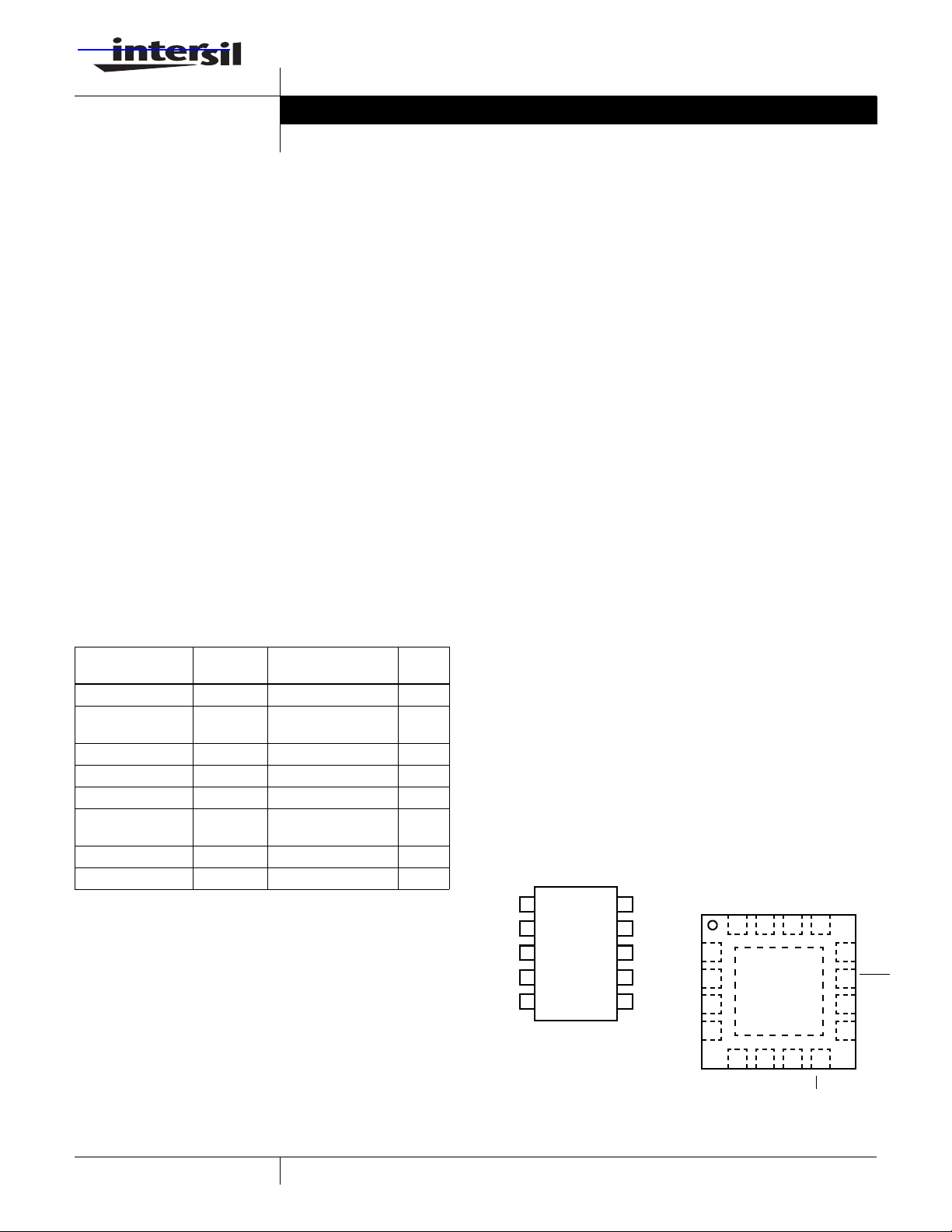
Ordering Information
TEMP.
PART NUMBER*
RANGE (°C) PACKAGE
ISL6410IR -40 to 85 16 Ld 4x4 QFN L16.4x4
ISL6410IRZ (Note) -40 to 85 16 Ld 4x4 QFN
(Pb-free)
ISL6410IU -40 to 85 10 Ld MSOP M10.118
ISL6410IUZ (Note) -40 to 85 10 Ld MSOP (Pb-free) M10.118
ISL6410AIR -40 to 85 16 Ld 4x4 QFN L16.4x4
ISL6410AIRZ (Note) -40 to 85 16 Ld 4x4 QFN
(Pb-free)
ISL6410AIU -40 to 85 10 Ld MSOP M10.118
ISL6410AIUZ (Note) -40 to 85 10 Ld MSOP (Pb-free) M10.118
*For tape and reel, add “-T”, “-TK” or “-T5K” suffix.
NOTE: Intersil Pb-free products employ special Pb-free material
sets; molding compounds/die attach materials and 100% matte tin
plate termination finish, which is compatible with both SnPb and
Pb-free soldering operations. Intersil Pb-free products are MSL
classified at Pb-free peak reflow temperatures that meet or exceed
the Pb-free requirements of IPC/JEDEC J Std-020B.
PKG.
DWG. #
L16.4x4
L16.4x4
FN9149.3
Features
• Fully Integrated Synchronous Buck Regulator
• PWM Fixed Output Voltage Options
- 1.8V, 1.5V or 1.2V with ISL6410 (VIN = 3.3V)
- 3.3V, 1.8V or 1.2V with ISL6410A (VIN = 5.0V)
• Continuous Output Current . . . . . . . . . . . . . . . . . . 600mA
• Ultra-Compact DC-DC Converter Design
• Stable with Small Ceramic Output Capacitors
• High Conversion Efficiency
• Extensive Circuit Protection and Monitoring features
- Overvoltage, UVLO
- Overcurrent
- Thermal Shutdown
• Available in MSOP and QFN packages
• QFN Package:
- Compliant to JEDEC PUB95 MO-220
QFN - Quad Flat No Leads - Package Outline
- Near Chip Scale Package footprint, which improves
PCB efficiency and has a thinner profile
• Pb-Free Packaging Available
Applications
• CPUs, DSP, CPLDs, FPGAs
• ASICs
• DVD and DSL applications
•WLAN Cards
• Generic 5V to 3.3V Conversion
Pinouts
ISL6410 (MSOP)
PVCC
1
VIN
2
GND
3
PG
4
FB
5
TOP VIEW
PGND
10
L
9
VIN
EN
8
SYNC
7
VSET
6
CT
GND
PG
ISL6410 (QFN)
TOP VIEW
VIN
PVCC
16 14 13
15
1
2
3
4
L
PGND
12
NC
RESET
11
10
EN
9
SYNC
6578
FB
NC
1
CAUTION: These devices are sensitive to electrostatic discharge; follow proper IC Handling Procedures.
1-888-INTERSIL or 321-724-7143
| Intersil (and design) is a registered trademark of Intersil Americas Inc.
All other trademarks mentioned are the property of their respective owners.
Copyright © Intersil Americas Inc. 2004. All Rights Reserved
PG
VSET
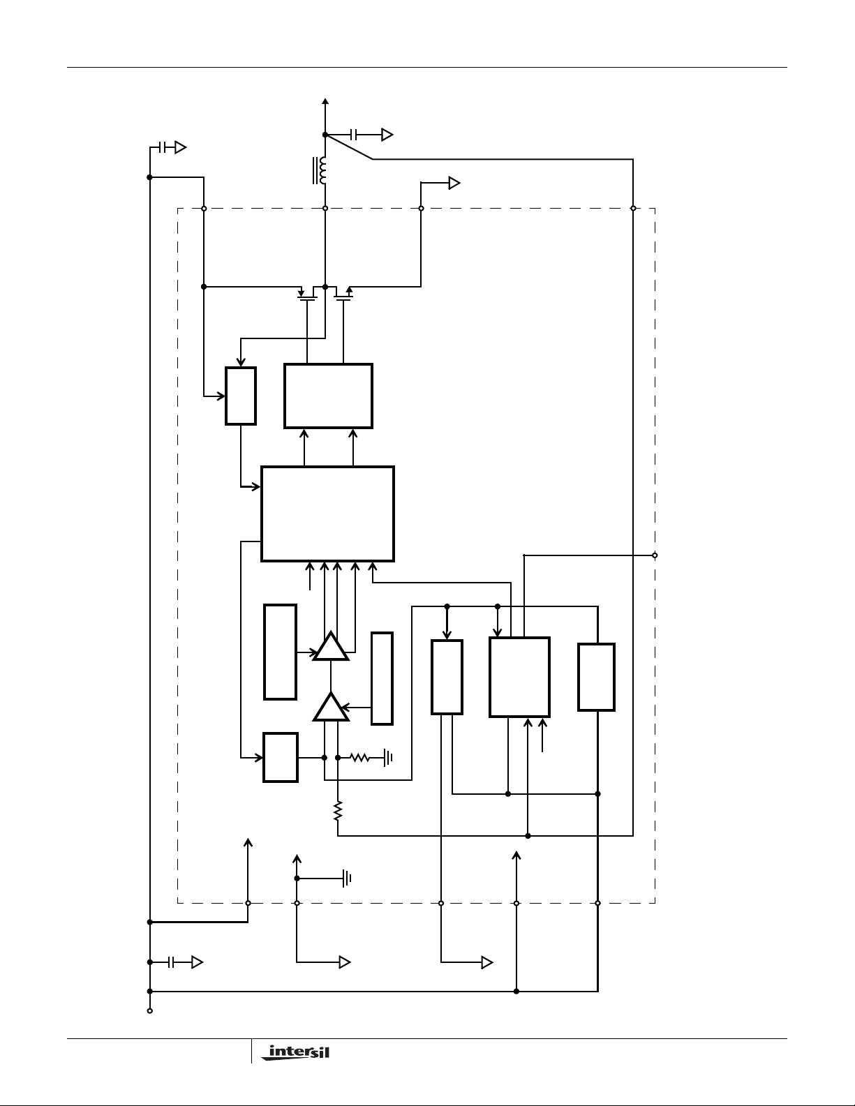
ISL6410, ISL6410A
0.1µF
VOUT
L1
8.2µH
1
PVCC
SENSE
CURRENT
10µF
9
L
GATE
DRIVE
10
PGND
5
FB
VIN
2
SLOPE
SOFT
COMPENSATION
START
GND
3
EN
PWM
OVERCURRENT,
OVERVOLTAGE
GM
EA
LOGIC
PG
4
POWER GOOD
PWM
OUT
UVLO
V
VSET
6
750kHz
COMPENSATION
OSCILLATOR
SYNC
7
PWM
0.45V
REFERENCE
EN
8
1. VIN is 3.3V for ISL6410 and 5.0V for ISL6410A.
NOTES:
2. VSET in the above schematic is connected to VIN, so the VOUT is 1.8V for ISL6410 and 3.3V for ISL6410A.
Functional Block Diagram for MSOP Version
10µF
VIN
2
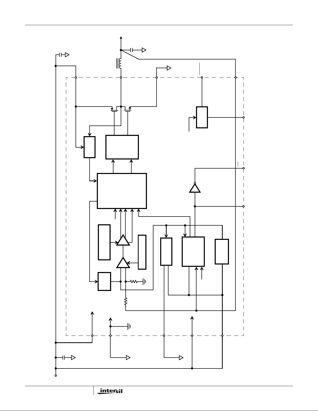
ISL6410, ISL6410A
0.1µF
VOUT
L1
8.2µH
15
PVCC
SENSE
CURRENT
10µF
14
L
GATE
DRIVE
13
PGND
RESET
11
RESET
BLOCK
IN
V
5
FB
T
C
2
PG
8
VIN
16
SLOPE
SOFT
COMPENSATION
START
GND
3
EN
PWM
OVERCURRENT,
OVERVOLTAGE
GM
EA
LOGIC
PG
4
POWER GOOD
PWM
OUT
UVLO
V
VSET
7
750kHz
COMPENSATION
OSCILLATOR
SYNC
9
PWM
0.45V
REFERENCE
EN
10
1. VIN is 3.3V for ISL6410 and 5.0V for ISL6410A.
NOTES:
2. VSET in the above schematic is connected to VIN, so the VOUT is 1.8V for ISL6410 and 3.3V for ISL6410A.
Functional Block Diagram for QFN Version
10µF
VIN
3
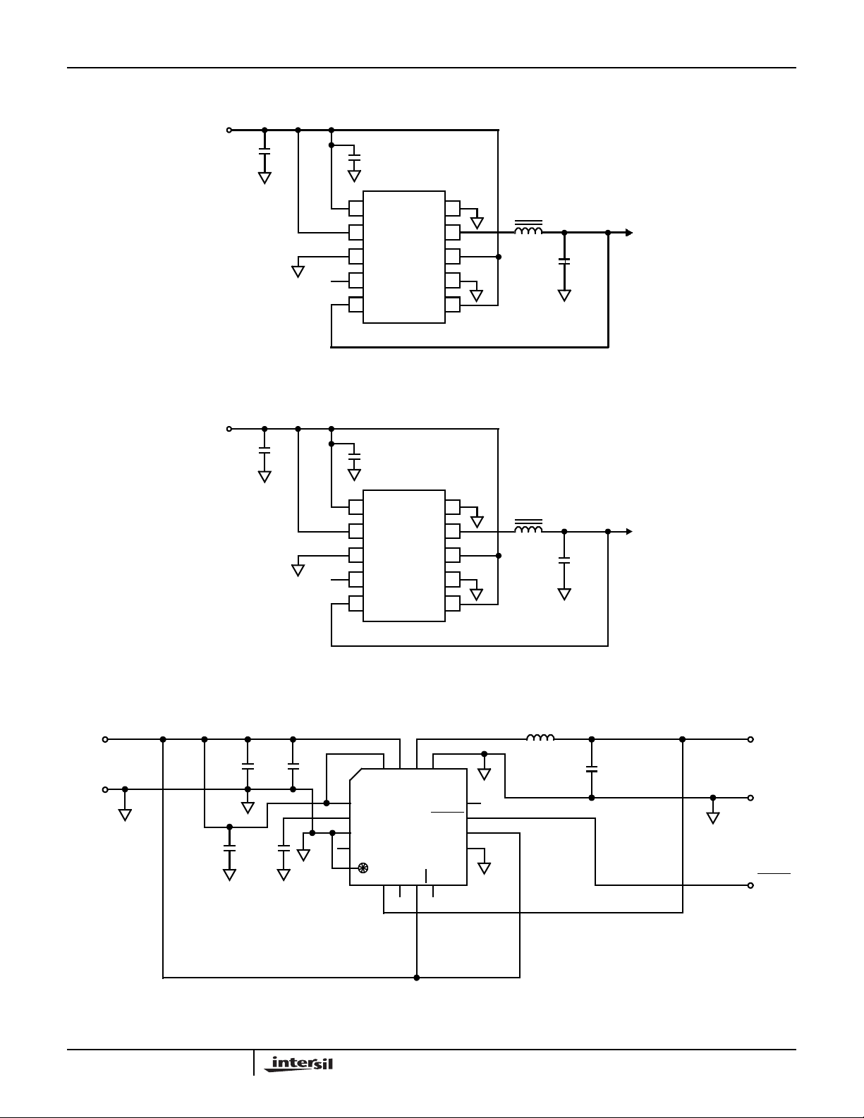
Typical Application Schematics
VIN
3.3V
±10%
C
IN
10µF
ISL6410, ISL6410A
0.1µF
VIN
5.0V
±10%
C
10µF
1
2
3
4
5
PVCC
VIN
GND
PG
FB
PGND
ISL6410
SYNC
VSET
EN
10
L
9
8
7
6
L1
8.2µH
C
OUT
10µF
V
OUT
1.8V
FIGURE 1. SCHEMATIC USING THE ISL6410 MSOP
IN
1
2
3
4
5
0.1µF
PVCC
VIN
GND
PG
FB
PGND
ISL6410A
SYNC
VSET
EN
10
L
9
8
7
L1
12µH
C
OUT
10µF
V
OUT
3.3V
6
+3.3V
VIN
GND
C7
0.1µF
C
10µF
IN
4
C
0.01µF
FIGURE 2. SCHEMATIC USING THE ISL6410A MSOP
1
VIN
2
CT
3
GND
4
PG
17
16 15 14 13
EP
567 8
L
VIN
PVCC
U1
ISL6410IR
NC
FB
VSET
PGND
NC
RESET
EN
SYNC
PG
12
11
10
9
1µF
T
FIGURE 3. SCHEMATIC USING THE ISL6410 QFN
L1
8.2µH
C
OUT
10µF
+1.2V
VOUT
GND
RESET
BAR

ISL6410, ISL6410A
Absolute Maximum Ratings Thermal Information
Supply Voltage, VCC . . . . . . . . . . . . . . . . . . . . . . . . . -0.3V to +6.0V
SYNC, FB, VSET & Enable Input (Note 3) . . . . -0.3V to VCC + 0.3V
ESD Classification (Human Body Model) . . . . . . . . . . . . . . . Class 2
CAUTION: Stresses above those listed in “Absolute Maximum Ratings” may cause permanent damage to the device. This is a stress only rating and operation of the
device at these or any other conditions above those indicated in the operational sections of this specification is not implied.
NOTES:
3. All voltages are with respect to GND.
is measured in free air with the component mounted on a high effective thermal conductivity test board with “direct attach” features. See
4. θ
JA
Tech Brief TB379.
5. For θ
, the “case temp” location is the center of the exposed metal pad on the package underside.
JC
Thermal Resistance (Typical) θ
(°C/W) θJC (°C/W)
JA
MSOP Package (Note 4) . . . . . . . . . . . 128 NA
QFN Package (Notes 4, 5). . . . . . . . . . 45 7.5
Maximum Junction Temperature (Plastic Package) . . . . . . . . 150°C
Maximum Storage Temperature Range. . . . . . . . . . . -65°C to 150°C
Maximum Lead Temperature (10s, soldering . . . . . . . . . . . . . 260°C
Ambient Temperature Range. . . . . . . . . . . . . . . . . . . . -40°C to 85°C
Junction Temperature Range. . . . . . . . . . . . . . . . . . . -40°C to 125°C
Electrical Specifications Recommended operating conditions unless otherwise noted. V
(ISL6410A), T
= 25°C (Note 6).
A
= 3.3V ±10% (ISL6410) or 5V ±10%
IN
PARAMETER TEST CONDITIONS MIN TYP MAX UNITS
V
SUPPLY
CC
Supply Voltage Range VIN (ISL6410) 3.0 3.3 3.6 V
VIN (ISL6410A) 4.5 5.0 5.5 V
Input UVLO Threshold V
Quiescent Supply Current I
Shutdown Supply Current EN = GND, T
(ISL6410) Rising 2.62 2.68 2.73 V
TR
V
(ISL6410) Falling 2.53 2.59 2.64 V
TF
V
(ISL6410A) Rising 4.27 4.37 4.45 V
TR
V
(ISL6410A) Falling 4.1 4.22 4.32 V
TF
= 0mA - 2.3 - mA
OUT
= 25°C - 5 10 µA
A
EN = GND, T
= 85°C - 10 15 µA
A
Thermal Shutdown Temperature (Note 7) Rising Threshold - 150 - °C
Thermal Shutdown Hysteresis (Note 7) - 20 25 °C
SYNCHRONOUS BUCK PWM REGULATOR
Output Voltage ISL6410, VSET = L - 1.2 - V
ISL6410, VSET = H - 1.8 - V
ISL6410, VSET = OPEN - 1.5 - V
ISL6410A, VSET = L - 1.2 - V
ISL6410A, VSET = H - 3.3 - V
ISL6410A, VSET = OPEN - 1.8 - V
Output Voltage Accuracy I
Line Regulation I
Load Regulation I
= 3mA, TA = -40°C to 85°C -1.5 - +1.5 %
OUT
= 3mA -0.5 - +0.5 %
OUT
= 3mA to 600mA -1.5 - +1.5 %
OUT
Maximum Output Current - - 600 mA
Peak Output Current Limit 700 - 1300 mA
PMOS r
DS(ON)
NMOS r
DS(ON)
Efficiency I
I
= 200mA - 230 - mΩ
OUT
I
= 200mA - 230 - mΩ
OUT
= 200mA, VIN = 3.3V, VO = 1.8V (ISL6410) - 92 - %
OUT
5

ISL6410, ISL6410A
Electrical Specifications Recommended operating conditions unless otherwise noted. V
(ISL6410A), T
= 25°C (Note 6). (Continued)
A
= 3.3V ±10% (ISL6410) or 5V ±10%
IN
PARAMETER TEST CONDITIONS MIN TYP MAX UNITS
Efficiency I
Efficiency I
= 200mA, VIN = 5.0V, VO = 3.3V (ISL6410A) - 93 - %
OUT
= 600mA, VIN = 5.0V, VO = 3.3V (ISL6410A) - 91 - %
OUT
Soft-Start Time 4096 Clock Cycles @ 750kHz - 5.5 - ms
OSCILLATOR
Oscillator Frequency 620 750 860 kHz
Frequency Synchronization Range (f
) Clock signal on SYNC pin 500 - 1000 kHz
SYNC
SYNC High Level Input Voltage As % of VIN 70 - - %
SYNC Low Level Input Voltage As % of VIN - - 30 %
Sync Input Leakage Current SYNC = GND or V
IN
-1 - 1 µA
Duty Cycle of External Clock Signal (Note 7) 20 - 60 %
PGOOD (ISL6410 interfaces to 3.3V Logic, ISL6410A interfaces to 5.0V Logic)
Rising Threshold 1mA minimum source/sink +5.0 8.0 +10.5 %
Falling Threshold -10.5 -8.0 -5.0 %
Rising/Falling Hysteresis -1 - %
ENABLE
EN High Level Input Voltage As % of VIN 70 - - %
EN Low Level Input Voltage As % of VIN - - 30 %
EN Input Leakage Current EN = GND or V
IN
-1 1 µA
OVERVOLTAGE
Overvoltage Threshold 27 30 33 %
RESET BLOCK SPECIFICATIONS
RESET (reset released) ISL6410, ISOURCE = 500µA, VIN = 2.90V 0.8V
IN
- - V
RESET (reset asserted) ISL6410, ISINK = 1.2mA, VIN = 2.50V - - 0.3 V
RESET Rising Threshold ISL6410 2.74 2.78 2.81 V
RESET Falling Threshold ISL6410 2.72 2.77 2.79 V
RESET (reset released) ISL6410A, ISOURCE = 800µA, VIN = 4.70V 0.8V
IN
-- V
RESET (reset asserted) ISL6410A, ISINK = 3.2mA, VIN = 4.10V - - 0.4 V
RESET Rising Threshold ISL6410A 4.5 4.58 4.64 V
RESET Falling Threshold ISL6410A 4.47 4.55 4.61 V
RESET Threshold Hysteresis ISL6410 - 20 - mV
RESET Threshold Hysteresis ISL6410A - 30 - mV
RESET Active Timeout Period (Note 8) CT = 0.01mF - 25 - ms
V
SET
V
High Level Input VIN-0.4V - - V
SET
V
Low Level Input --0.4V
SET
V
Open Level Input -VIN/2 - V
SET
NOTES:
6. Specifications at -40°C and +85°C are guaranteed by design, not production tested.
7. Guaranteed by design, not production tested.
8. The RESET Timeout period is linear with C
at a slope of 2.5ms/nF, thus a 10nF capacitor provides for 25ms.
T
6

ISL6410, ISL6410A
Pin Description
VIN - Supply voltage for the IC. It is recommended to place a
1µF decoupling capacitor as close as possible to the IC.
GND - Small signal ground for the PWM controller stage. All
internal control circuits are referenced to this pin.
PG - The Power good is an open-drain output. A pull-up
resistor should be connected between PG and VIN. It is
asserted active high when the output voltage reaches
94.5% of the nominal value.
FB - The Feedback pin is used to sense the output voltage,
and should be connected to VOUT for normal operation.
VSET - This pin is used to program the output voltages.
Refer to Table 1 below for details.
TAB L E 1 .
ISL6410
VSET
High 1.8V 3.3V
Open (NC) 1.5V 1.8V
Low 1.2V 1.2V
SYNC - This pin is used for synchronization. The converter
switching frequency can be synchronized to an external
CMOS clock signal in the range of (500kHz to 1MHz).
EN - A logic high enables the converter, logic low forces the
device into shutdown mode reducing the supply current to
less than 10
via a 10K resistor.
L - This pin is the drain junction of the internal power
MOSFETs and is to be connected to the external inductor.
PGND - Power ground. Connect all power grounds to this pin.
PVCC - This pin provides the Input supply for the internal
MOSFETs. It is recommended to place a 1µF decoupling
capacitor as close as possible to the IC.
CT - Timing capacitor connection to set the 25ms minimum
pulse width for the RESET
RESET - The outputs of the reset supervisory circuit, which
monitors VIN. The IC asserts these RESET
whenever the supply voltage drops below a preset threshold
and keeps it asserted for at least 25ms after VCC (VIN) has
risen above the reset threshold. These outputs are pushpull. RESET
The PWM will continue to operate until VIN drops below the
UVLO threshold.
µA at 25°C. This pin should be pulled up to VCC
is LOW when re-setting the microprocessor.
Vo
signal.
ISL6410A
Vo
signals
efficiency and reduced number of external components.
Operating frequency of 750kHz typical allows the use of
small inductor and capacitor values. The device can be
synchronized to an external clock signal in the range of
500kHz to 1MHz. The PG output indicates loss of regulation
on PWM output.
The PWM is based on the peak current mode control
topology with internal slope compensation. At the beginning
of each clock cycle, the high side P-channel MOSFET is
turned on. The current in the inductor ramps up and is
sensed via an internal circuit. On exceeding a preset limit the
high side switch is turned off causing the PWM comparator
to trip. This occurs whenever the output voltage is in
regulation or when the inductor current reaches the current
limit. After a minimum dead time to prevent shoot through
current, the low side N-channel MOSFET turns on and the
current ramps down. As the clock cycle is completed, the low
side switch turns off and the next clock cycle is initiated.
The control loop is internally compensated thus reducing the
amount of external components.
The switch current is internally sensed and the maximum
current limit is 1300mA peak.
Synchronization
The typical operating frequency for the converter is 750kHz.
It is possible to synchronize the converter to an external
clock frequency in the range of 500kHz to 1000kHz when an
external signal is applied to SYNC pin. The device will
automatically detect and synchronize to the rising edge of
the first clock pulse. If the clock signal is stopped, the
converter automatically switches back to the internal clock
and continues its operation without interruption. The switch
over will be initiated if no rising edge triggers are present on
the SYNC pin for a duration of four clock cycles.
Soft-Start
As the EN (Enable) pin goes high, the soft-start function will
generate an internal voltage ramp. This causes the start-up
current to slowly rise preventing output voltage overshoot
and high inrush currents. The soft-start duration is typically
5.5ms with 750kHz switching frequency. When the soft-start
is completed, the error amplifier will be connected directly to
the internal voltage reference.
Enable
Logic low on EN pin forces the PWM section into shutdown.
In the shutdown mode all the major blocks of the PWM
including power switches, drivers, voltage reference, and
oscillator are turned off.
Functional Description
The ISL6410, ISL6410A is a synchronous buck regulator
with integrated N- and P-channel power MOSFET and
provides pre-set pin programmable outputs. Synchronous
rectification with internal MOSFETs is used to achieve higher
7
Undervoltage Lockout
An undervoltage lockout circuit prevents the converter from
turning on when the voltage on VIN is less than the values
specified in the Input UVLO Threshold section of the
electrical specification.

ISL6410, ISL6410A
Power Good
This output is asserted high when the PWM is enabled, and
Vout is within 8.0% typical of its final value, and is active low
outside this range. When disabled, the output turns active
low. It is recommended to leave the PG pin unconnected
when not used.
PWM Overvoltage and Overcurrent Protection
The PWM output current is sampled at the end of each PWM
cycle, exceeding the overcurrent limit, causes a 4 bit
up/down counter to increment by one LSB. A normal current
state causes the counter to decrement by one LSB (the
counter will not however “rollover” or count below 0000).
When the PWM goes into overcurrent, the counter rapidly
reaches count 1111 and the PWM output is shut down and
the soft-start counter is reset. After 16 clocks the PWM
output is enabled and the soft-start cycle is started.
If Vout exceeds the overvoltage limit for 32 consecutive clock
cycles the PWM output is shut off and the soft-start cycle is
initiated.
No Load Operation
If there is no load connected to the output, the converter will
regulate the output voltage by allowing the inductor current
to reverse for a short period of time.
Output Capacitor Selection
For best performance, a low ESR output capacitor is
needed. Output voltages below 1.8V require a larger output
capacitor and ESR value to improve the performance and
stability of the converter. For 1.8V output applications, a
ceramic capacitor of 10µF or higher value with ESR ≤50mΩ
is recommended.
The RMS ripple current is calculated as:
Vo
1
---------–
I
RMS Co()
Vo
------------------ -
Lf×
Vin
L = the inductor value
f = the switching frequency
The overall output ripple voltage is the sum of the voltage spike
caused by the output capacitor ESR and the voltage ripple
caused by charge and discharge of the output capacitor:
Vo
1
---------–
Vin
Vo∆ Vo
------------------ -
Lf×
××=
Where the highest output voltage ripple occurs at the highest
input voltage VIN.
1
---------------- -
××=
23×
1
------------------------- ESR+
8Cof××
Input Capacitor Selection
The input current to the buck converter is pulsed, and
therefore a low ESR input capacitor is required. This results
in good input voltage filtering and minimizes the interference
it causes to other circuits. The input capacitor should have a
minimum value of 10µF and a higher value can be selected
for improving input voltage filtering. The input capacitor
should be rated for the maximum input ripple current
calculated as:
I
RMS
Io max()
Vo
---------
Vin
Vo
1
---------–
××=
Vin
The worst case RMS ripple current occurs at D = 0.5 and is
calculated as: Irms = Io/2.
D = Duty Cycle
Ceramic capacitors are preferred because of their low ESR
value. They are also less sensitive to voltage transients
when compared to tantalum capacitors. It is good practice to
place the input capacitor as close as possible to the input pin
of the IC for optimum performance.
Inductor Selection
The ISL6410 is an internally compensated device and hence
a minimum of 8.2
minimum of 12
must have a low DC resistance and a saturation current
greater than the maximum inductor current value can be
calculated from the equations below
dIL Vo
IL max Io max
×=
where
dIL = the peak to peak inductor current
L = the inductor value
f = the switching frequency
ILmax = the max inductor current
INDUCTOR VALUE DCR (mΩ)
8.2µH75Coilcraft
12µH 100 Coilcraft
µH must be used for the ISL6410 and a
µH for the ISL6410A. The selected inductor
Vo
1
---------–
Vin
------------------ -
Lf×
dIL
-------- -+=
2
TABLE 3. RECOMMENDED INDUCTORS
COMPONENT
SUPPLIER
MSS6122-822MX
MSS6122-123MX
TABLE 2. RECOMMENDED OUTPUT CAPACITORS
CAPACITOR
VAL UE
10µF <50 AVX 08056D106KAT2A Ceramic
ESR
(mΩ)
COMPONENT
SUPPLIER COMMENTS
8

ISL6410, ISL6410A
Layout Considerations
As in all switching power supplies, the layout is an important
step in the design process, more so at high peak currents
and switching frequencies. Improper layout practice will give
rise to Stability and EMI issues. It is recommended that wide
and short traces are used for the main current paths. The
Performance Curves and Waveforms
100
VOUT = 1.8V
90
80
VOUT = 1.5V
VOUT = 1.2V
input capacitor should be placed as close as possible to the
IC pins. This applies to the output inductor and capacitor as
well. The analog ground, GND, and the power ground,
PGND, need to be separated. Use a common ground node
to minimize the effects of ground noise.
100
IOUT = 200mA
90
IOUT = 600mA
80
70
EFFICIENCY (%)
60
50
IOUT LOAD CURRENT (mA)
100010050
70
EFFICIENCY (%)
60
50
3.1 3.5
VIN INPUT VOLTAGE (V)
3.32.9
FIGURE 4. ISL6410 EFFICIENCY vs LOAD CURRENT FIGURE 5. ISL6410 VIN vs EFFICIENCY
100
VOUT = 3.3V
90
80
70
EFFICIENCY (%)
60
50
VOUT = 1.2V
IOUT LOAD CURRENT (mA)
VOUT = 1.8V
100010050
100
IOUT = 200mA
90
IOUT = 600mA
80
70
EFFICIENCY (%)
60
50
4.6
4.8 5.2
VIN (V)
FIGURE 6. ISL6410A EFFICIENCY vs LOAD CURRENT FIGURE 7. ISL6410A EFFICIENCY vs VIN
5.4
5.65.04.4
9

ISL6410, ISL6410A
Performance Curves and Waveforms (Continued)
800
780
790
780
770
760
SWITCHING FREQUENCY (kHz)
750
-15
10 60
TEMPERATURE (°C)
FIGURE 8. ISL6410 OSCILLATOR FREQUENCY vs
TEMPERATURE
CH1 = Top, CH2 = Middle, CH4 = Bottom, where applicable
VOUT
L PIN VOLTAGE
770
760
750
740
SWITCHING FREQUENCY (kHz)
8535-40
730
-15
10 60
TEMPERATURE (°C)
8535-40
FIGURE 9. ISL6410A OSCILLATOR FREQUENCY vs
TEMPERATURE
VOUT
L PIN VOLTAGE
L1 CURRENT
CH1 = 0.1V/DIV, CH2 = 2V/DIV CH4 = 200mA/DIV
0.5µs/DIV
L1 CURRENT
VIN = 5.0V, VOUT = 1.2V, IOUT = 0.5A
CH1 = 0.1V/DIV, CH2 = 2V/DIV CH4 = 200mA/DIV
0.5µs/DIV
FIGURE 10. SWITCHING WAVEFORM FOR ISL6410 FIGURE 11. SWITCHING WAVEFORM FOR ISL6410A
VOUT
IOUT
VIN = 3.3V, VOUT = 1.2V
0.5ms/DIV
CH1 = 0.2V/DIV, CH4 = 200mA/DIV
VOUT
IOUT
VIN = 5.0V, VOUT = 1.2V
0.5ms/DIV
CH1 = 0.1V/DIV, CH4 = 200mA/DIV
FIGURE 12. TRANSIENT LOAD WAVEFORM FOR ISL6410 FIGURE 13. TRANSIENT LOAD WAVEFORM FOR ISL6410A
10

ISL6410, ISL6410A
Performance Curves and Waveforms (Continued)
VOUT
VIN = 3.3V, VOUT = 1.2V
1µs/DIV
CH1 = 20mV/DIV
VOUT
VIN = 5.0V, VOUT = 1.2V
1µs/DIV
CH1 = 20mV/DIV
FIGURE 14. RIPPLE WAVEFORM FOR ISL6410 FIGURE 15. RIPPLE WAVEFORM FOR ISL6410A
-40
-50
-60
-70
-80
-90
-100
-110
-120
NOISE LEVEL 761kHz = -54.0dBm
CENTER 2.75MHz, SPAN = 4.5MHz
VIN = 3.3V, VOUT = 1.2V
FIGURE 16. SWITCHING HARMONICS AND NOISE FOR
ISL6410
-40
VIN = 5.0V, VOUT = 1.2V
-50
-60
-70
-80
-90
-100
-110
-120
NOISE LEVEL 732kHz = -65.3dBm
CENTER 2.75MHz, SPAN = 4.5MHz
FIGURE 17. SWITCHING HARMONICS AND NOISE FOR
ISL6410A
11

ISL6410, ISL6410A
Quad Flat No-Lead Plastic Package (QFN)
Micro Lead Frame Plastic Package (MLFP)
L16.4x4
16 LEAD QUAD FLAT NO-LEAD PLASTIC PACKAGE
(COMPLIANT TO JEDEC MO-220-VGGC ISSUE C)
MILLIMETERS
SYMBOL
A 0.80 0.90 1.00 A1 - - 0.05 A2 - - 1.00 9
A3 0.20 REF 9
b 0.23 0.28 0.35 5, 8
D 4.00 BSC D1 3.75 BSC 9
D2 1.95 2.10 2.25 7, 8
E 4.00 BSC E1 3.75 BSC 9
E2 1.95 2.10 2.25 7, 8
e 0.65 BSC -
k0.25 - - -
L 0.50 0.60 0.75 8
L1 - - 0.15 10
N162
Nd 4 3
Ne 4 3
P- -0.609
θ --129
NOTES:
1. Dimensioning and tolerancing conform to ASME Y14.5-1994.
2. N is the number of terminals.
3. Nd and Ne refer to the number of terminals on each D and E.
4. All dimensions are in millimeters. Angles are in degrees.
5. Dimension b applies to the metallized terminal and is measured
between 0.15mm and 0.30mm from the terminal tip.
6. The configuration of the pin #1 identifier is optional, but must be
located within the zone indicated. The pin #1 identifier may be
either a mold or mark feature.
7. Dimensions D2 and E2 are for the exposed pads which provide
improved electrical and thermal performance.
8. Nominal dimensions are provided to assist with PCB Land Pattern
Design efforts, see Intersil Technical Brief TB389.
9. Features and dimensions A2, A3, D1, E1, P & θ are present when
Anvil singulation method is used and not present for saw
singulation.
10. Depending on the method of lead termination at the edge of the
package, a maximum 0.15mm pull back (L1) maybe present. L
minus L1 to be equal to or greater than 0.3mm.
NOTESMIN NOMINAL MAX
Rev. 5 5/04
12

ISL6410, ISL6410A
Mini Small Outline Plastic Packages (MSOP)
N
EE1
INDEX
AREA
AA1A2
-H-
SIDE VIEW
12
TOP VIEW
b
e
D
NOTES:
1. These package dimensions are within allowable dimensions of
JEDEC MO-187BA.
2. Dimensioning and tolerancing per ANSI Y14.5M-1994.
3. Dimension “D” does not include mold flash, protrusions or gate
burrs and are measured at Datum Plane. Mold flash, protrusion
and gate burrs shall not exceed 0.15mm (0.006 inch) per side.
4. Dimension “E1” does not include interlead flash or protrusions
and are measured at Datum Plane. Interlead flash and
protrusions shall not exceed 0.15mm (0.006 inch) per side.
5. Formed leads shall be planar with respect to one another within
0.10mm (.004) at seating Plane.
6. “L” is the length of terminal for soldering to a substrate.
7. “N” is the number of terminal positions.
8. Terminal numbers are shown for reference only.
9. Dimension “b” does not include dambar protrusion. Allowable
dambar protrusion shall be 0.08mm (0.003 inch) total in excess
of “b” dimension at maximum material condition. Minimum space
between protrusion and adjacent lead is 0.07mm (0.0027 inch).
- H -
-A -
.
10. Datums and to be determined at Datum plane
11. Controlling dimension: MILLIMETER. Converted inch dimensions are for reference only
-B-
0.20 (0.008) A
GAUGE
PLANE
SEATING
PLANE
0.10 (0.004) C
-A-
0.20 (0.008) C
- B -
0.25
(0.010)
-C-
SEATING
PLANE
a
0.20 (0.008) C
- H -
B
4X θ
C
D
4X θ
L1
C
C
L
E
1
END VIEW
R1
R
L
-B-
M10.118 (JEDEC MO-187BA)
10 LEAD MINI SMALL OUTLINE PLASTIC PACKAGE
INCHES MILLIMETERS
SYMBOL
A 0.037 0.043 0.94 1.10 A1 0.002 0.006 0.05 0.15 A2 0.030 0.037 0.75 0.95 -
b 0.007 0.011 0.18 0.27 9
c 0.004 0.008 0.09 0.20 -
D 0.116 0.120 2.95 3.05 3
E1 0.116 0.120 2.95 3.05 4
e 0.020 BSC 0.50 BSC -
E 0.187 0.199 4.75 5.05 -
L 0.016 0.028 0.40 0.70 6
L1 0.037 REF 0.95 REF -
N10 107
R 0.003 - 0.07 - -
R1 0.003 - 0.07 - -
o
θ
α
5
o
0
15
o
o
6
o
5
o
0
15
o
o
6
Rev. 0 12/02
NOTESMIN MAX MIN MAX
-
-
All Intersil U.S. products are manufactured, assembled and tested utilizing ISO9000 quality systems.
Intersil Corporation’s quality certifications can be viewed at www.intersil.com/design/quality
Intersil products are sold by description only. Intersil Corporation reserves the right to make changes in circuit design, software and/or specifications at any time without
notice. Accordingly, the reader is cautioned to verify that data sheets are current before placing orders. Information furnished by Intersil is believed to be accurate and
reliable. However, no responsibility is assumed by Intersil or its subsidiaries for its use; nor for any infringements of patents or other rights of third parties which may result
from its use. No license is granted by implication or otherwise under any patent or patent rights of Intersil or its subsidiaries.
For information regarding Intersil Corporation and its products, see www.intersil.com
13
 Loading...