®
www.BDTIC.com/Intersil
ISL6405
Data Sheet July 2004
Dual Output LNB Supply and Control
Voltage Regulator with I2C Interface for
Advanced Satellite Set-Top Box Designs
The ISL6405 is a highly integrated voltage regulator and
interface IC, specifically designed for supplying power and
control signals from advanced satellite set-top box (STB)
modules to the low noise blocks (LNBs) of two antenna
ports. The device is comprised of two independent currentmode boost PWMs and two low-noise linear regulators along
with the circuitry required for 22kHz tone generation,
modulation and I
total LNB supply design simple, efficient and compact with
low external component count.
Two independent current-mode boost converters provide the
linear regulators with input voltages that are set to the final
output voltages, plus typically 1.2V to insure minimum power
dissipation across each linear regulator. This maintains
constant voltage drops across each linear pass element
while permitting adequate voltage range for tone injection.
The final regulated output voltages are available at two
output terminals to support simultaneous operation of two
antenna ports for dual tuners. The outputs for each PWM are
set to 13V or 18V by independent voltage select commands
(VSEL1, VSEL2) through the I
compensate for the voltage drop in the coaxial cable, the
selected voltage may be increased by 1V with the line length
compensation (LLC) feature. All the functions on this IC are
controlled via the I
Register (SR, 8 bits). The same register can be read back,
and two bits will report the diagnostic status. Separate enable
commands sent on the I
mode control for each PWM and linear combination, disabling
the output into shutdown mode.
Each output channel is capable of providing 750mA of
continuous current. The overcurrent limit can be digitally
programmed. The SEL18V pin with QFN package allows the
13V to 18V transition with an external pin, over-riding the I
input.
2
C device interface. The device makes the
2
C bus. Additionally, to
2
C bus by writing 8 bits on System
2
C bus provide independent standby
2
C
FN9026.2
Features
• Single Chip Power solution
- True Dual Operation for 2-Tuner/2-Dish Applications
- Both Outputs May be Enabled Simultaneously at
Maximum Power
- Integrated DC-DC Converter and I
• Switch-Mode Power Converter for Lowest Dissipation
- Boost PWMs with > 92% Efficiency
- Selectable 13V or 18V Outputs
- Digital Cable Length Compensation (1V)
2
•I
C Compatible Interface for Remote Device Control
- Registered Slave Address 0001 00XX
- Full 3.3V/5V Operation up to 400kHz
• External Pins to Select 13V/18V Options
- Available with QFN Package Only
• Built-In Tone Oscillator Factory Trimmed to 22kHz
- Facilitates DiSEqC
• Internal Over-Temperature Protection and Diagnostics
• Internal Overload and Overtemp Flags (Visible on I
• LNB Short-Circuit Protection and Diagnostics
• QFN Package
- Compliant to JEDEC PUB95 MO-220 QFN - Quad Flat
No Leads - Product Outline
- Near Chip-Scale Package Footprint
• Pb-free Packaging Available
- Designated with “Z” Suffix (Refer to Note Below)
(EUTELSAT) Encoding
TM
2
C Interface
2
C)
Applications
• LNB Power Supply and Control for Satellite Set-Top Box
References
• Tech Brief 389 (TB389) - “PCB Land Pattern Design and
Surface Mount Guidelines for QFN Packages”; Available
on the Intersil website, www.intersil.com
Ordering Information
PART # TEMP. RANGE (oC) PACKAGE PKG. DWG. #
ISL6405EEB -20 to 85 28 Ld EPSOIC M28.3B
ISL6405EEBZ
(Note 1)
ISL6405ER -20 to 85 32 Ld 5x5 QFN L32.5x5
ISL6405ERZ
(Note 1)
NOTES:
1. Intersil Pb-free products employ special Pb-free material sets; mo lding
compounds/die attach materials and 100% matte tin plate termination
finish, which is compatible with both SnPb and Pb-free soldering
operations. Intersil Pb-free products are MSL classified at Pb-free peak
reflow temperatures that meet or exceed the Pb-free requirements of
IPC/JEDEC J Std-020B.
2. Tape and Reel available. Add “-T” suffix for Tape and Reel Packing Option.
-20 to 85 28 Ld EPSOIC
(Pb-free)
-20 to 85 32 Ld 5x5 QFN
(Pb-free)
M28.3B
L32.5x5
1
CAUTION: These devices are sensitive to electrostatic discharge; follow proper IC Handling Procedures.
1-888-INTERSIL or 321-724-7143
| Intersil (and design) is a trademark of Intersil Americas Inc.
Copyright © Intersil Americas Inc. 2004. All Rights Reserved

VSW2
www.BDTIC.com/Intersil
COMP2
FB2
GATE2
PGND 2
CS2
SGND
BYPASS
PGND1
GATE1
CS1
FB1
COMP1
VSW1
ISL6405
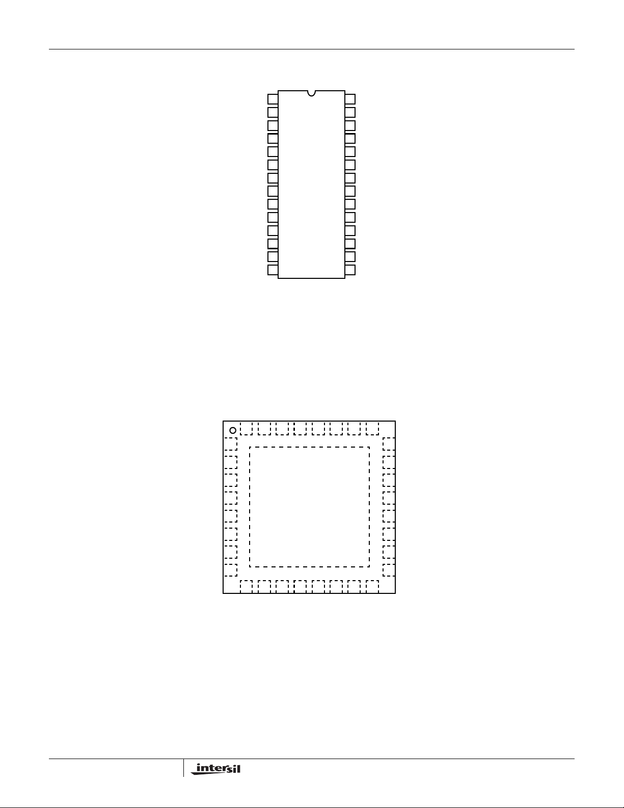
ISL6405 (EPSOIC)
TOP VIEW
1
2
3
4
5
6
ISL6405EEB
7
8
9
10
11
12
13
14
28
VCC
CPVOUT
27
CPSWIN
26
CPSWOUT
25
TCAP2
24
DSQIN2
23
VO2
22
AGND
21
20
VO1
DSQIN1
19
TCAP1
18
SCL
17
16
ADDR
SDA
15
PGND2
CS2
SGND
SEL18V1
SEL18V2
BYP
PGND1
GATE1
ISL6405 (QFN)
TOP VIEW
VCC
NC
FB2
GATE2
32 31 30 29 28 27 26 25
1
2
3
4
5
6
7
8
9 10111213141516
FB1
CS1
VSW2
COMP2
ISL6405ER
VSW1
COMP1
NC
SDA
CPVOUT
ADDR
SCL CPSWIN
24
23
22
21
20
19
18
17
CPSWOUT
TCAP2
DSQIN2
VO2
AGND
VO1
DSQIN1
TCAP1
2

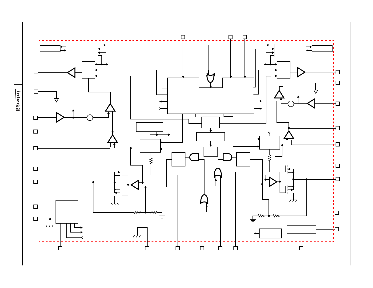
Block Diagram
www.BDTIC.com/Intersil
15 16 17
CLK1
SLOPE
OLF1
DCL
OC1
+
-
+
VREF1
BAND GAP
REF VOLTAGE
REF
VO LTAG E
ADJ1
+
-
SDA
SDA
ISEL1
EN1
ENT1
OTF
LLC1 VSEL1 VSEL2 LLC2
CLK1
BGV
TONE
INJ
CKT 1
OLF
I2C
INTERFACE
OSC.
220kHz
10 &
÷
WAVE SHAPING
22kHz
TONE
ENT2
CLK2
ADDR
SCLADDR
TONE
INJ
CKT 2
COUNTER
GATE1
10
3
PGND1
9
CS1
11
COMP1
13
FB1
12
VSW1
14
VO1
20
OVERCURRENT
PROTECTION
LOGIC SCHEME 1
ILIM1
CS
AMP
PWM
LOGIC
Q
S
∑
COMPENSATION
SCL
ISEL2
EN2
ENT2
DCL
OLF2
DCL
OC2
VOLTAGE
OVERCURRENT
LOGIC SCHEME 2
CLK2
BGV
REF
ADJ2
+
-
PROTECTION
PWM
LOGIC
Q
S
-
ILIM2
+
∑
SLOPE
COMPENSATION
+
-
VREF2
CS
AMP
COUNTER
GATE2
PGND2
CS2
COMP2
FB2
VSW2
VO2
4
5
6
2
ISL6405
3
1
22
VCC
28
SGND
7
ON CHIP
LINEAR
UVLO
POR
SOFT-START
BYPASS
8
INT 5V
SOFT-START
EN1/EN2
AGND
21
TCAP1
18 19
DSQIN1
ENT1
DSQIN2
23
OTF
TCAP2
24 25
THERMAL
SHUTDOWN
CHARGE PUMP
CPSWOUT
CPVOUT
CPSWIN
27
26

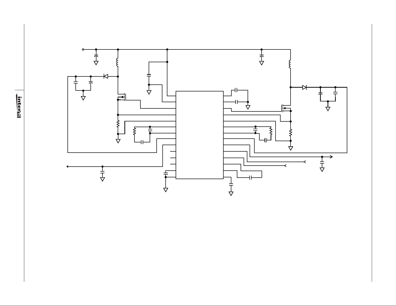
Typical Application Schematic
www.BDTIC.com/Intersil
VIN = 8V TO 14V
4
VO1
13V/18V
+
C3
L1
D1
+
C2C1
Q1
R1
C15
R2
C5
C4
C12
C16
28
7
10
11
9
13
12
14
20
19
23
16
18
21
VCC
SGND
GATE1
CS1
PGND1
COMP1
FB1
VSW1
VO1
DSQIN1
DSQIN2
ADDR
TCAP1
AGND
CPSWOUT
CPVOUT
ISL6405EEB
TCAP2
BYPASS
GATE2
CS2
PGND2
COMP2
FB2
VSW2
VO2
SCL
SDA
CPSWIN
C9
C20
24
C6
8
4
6
5
R3
2
3
1
22
17
15
26
25
27
C13
C8
+
C14
R3
C7
L2
SDA
R4
Q2
D2
SCL
+
C11C10
ISL6405
VO2
13V/18V
C17
 Loading...