

Page 1
®
www.BDTIC.com/Intersil
ISL6401
Data Sheet April 13, 2005
Synchronizing Current Mode PWM for
Subscriber Line Interface Circuits (SLICs)
The ISL6401 adjustable frequency, low power, pulse width
modulating (PWM) current mode controller is designed for a
wide range of DC/DC conversion applications including
boost, flyback, and isolated output configurations. The
device is optimized to provide a high performance, low-cost
solution for Ringing SLIC (RSLIC) ring and talk power
supplies. An integrated inverter allows for easy design of
negative voltage regulation circuits with a minimal amount of
external components. Internal soft-start minimizes start-up
stress without any external components. Peak current mode
control effectively handles Ring trip transients and provides
inherent overcurrent protection.
This advanced BiCMOS design features low operating
current, adjustable operating output frequency (50kHz to
600kHz), internal soft-start and a SYNC input that allows the
oscillator to be locked to an external clock for noise sensitive
applications. DC/DC conversion efficiency is optimized by
use of a low current sense voltage. A logic level shutdown
input is included, which reduces supply current to 55µA in
the shutdown mode.
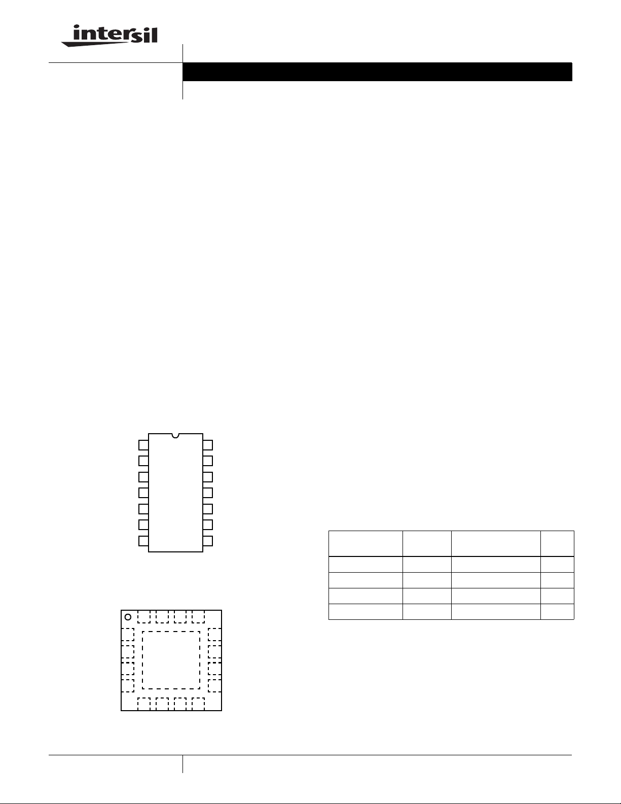
Pinouts
ISL6401 (SOIC)
TOP VIEW
SD
NFB OUT
SYNC
CT
COMP
FB
SYNC
CT
COMP
FB
NFB IN
1
2
3
4
1
2
3
4
5
6
7
ISL6401 (QFN)
TOP VIEW
SD
VCC
1516 14 13
6578
NFB IN
NFB OUT
PVCC
NC
14
13
12
11
10
GATE
NC
9
8
V
PV
GATE
PGND
GND
CS
NC
12
11
10
9
CC
CC
PGND
PGND
GND
CS
FN9007.7
Features
• Positive and Negative Output Regulation
• Starting Supply Current . . . . . . . . . . . . . . . . . 100µA (typ.)
• Quiescent Current . . . . . . . . . . . . . . . . . . . . . . 55µA (typ.)
• Output Frequency Range. . . . . . . . . . . . 50kHz to 600kHz
• External Clock Synchronization
• Fast Transient Response with Peak Current Mode Control
• Internal Soft-Start
• Drives N-Channel MOSFET
• Logic Level Shutdown
• Leading Edge Blanking
• 1% Tolerance Voltage Reference Over Line and
Temperature
• Pb-Free Available (RoHS Compliant)
Applications
• VoIP/VoDSL Ringer and Off-Hook Voltage Generators
• Multi-Output Flyback Supplies
• Cable and DSL Modems
• Set-Top Boxes
• Wireless Local Loops
• LMDH and FTTH Supplies
• Boost Regulators
•Routers
Ordering Information
PART NUMBER
ISL6401CB -40 to 85 14 Ld SOIC M14.15
ISL6401CBZ (Note) -40 to 85 14 Ld SOIC (Pb-free) M14.15
ISL6401CR -40 to 85 16 Ld 4x4 QFN L16.4x4
ISL6401CRZ (Note) -40 to 85 16 Ld 4x4 QFN (Pb-free) L16.4x4
Add -T suffix for tape and reel packaging.
NOTES:
1. The parts with suffix ‘C’ are being tested to the industrial temperature
grade. This has been updated in the table above. The IB and IR parts are
being discontinued. The affected parts are: ISL6401IB, ISL6401IBZ,
ISL6401IB-T, ISL6401IBZ-T, ISL6401IR, ISL6401IRZ, ISL6401IR-T,
ISL6401IRZ-T.
2. Intersil Pb-free products employ special Pb-free material sets; molding
compounds/die attach materials and 100% matte tin plate termination
finish, which are RoHS compliant and compatible with both SnPb and Pbfree soldering operations. Intersil Pb-free products are MSL classified at
Pb-free peak reflow temperatures that meet or exceed the Pb-free
requirements of IPC/JEDEC J STD-020.
TEMP.
RANGE (°C) PACKAGE
PKG.
DWG. #
1
CAUTION: These devices are sensitive to electrostatic discharge; follow proper IC Handling Procedures.
1-888-INTERSIL or 1-888-352-6832
| Intersil (and design) is a registered trademark of Intersil Americas Inc.
All other trademarks mentioned are the property of their respective owners.
Copyright © Intersil Americas Inc. 2001-2005. All Rights Reserved
Page 2
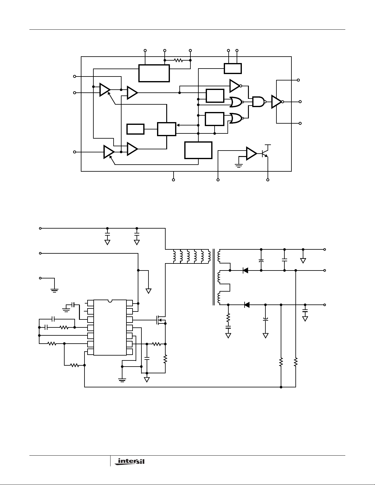
Functional Block Diagram
www.BDTIC.com/Intersil
ISL6401
VCCGND
VREF
4
5
9
FB
CS
COMP
ERROR
+
-
VREF
AMP
CS
VOLTAGE
REFERENCE
IBIAS
ICSCOMP
+
SOFT-START
POR
UVLO
+
ICLCOMP
LVC
SOFT-
START
200K
ILIM
ENPWM
Typical Application Schematic for 4 Line VoIP
VIN
9V TO
20V
+5V
±10%
GND
0.027µF
VCC
220pF
C6
C5
R2
10K
R1
20K
C4
560pF
E
R3
1.24K
C1A-E
2.2µF
35V
SD
1
2
SYNC
3
CT
4
COMP
5
FB
6
NFB
7 8
NFB_IN
PV
GATE
GNDP
ISL6401
V
CC
CC
GND
CS
NC
C2
1µF
50V
14
13
12
11
10
9
C3
1µF
16V
R6
100
C7
1000pF
8
000000
PRI
1
Q1
IRLR2905
R5
0.025
1W
11410
SD
CLK
LEADING
EDGE
BLANKING
S
RQ
TFF
CLKRQ
T1
IFLY0012
CT SYNC
OSC
NFB_IN
768NC
2
SEC
7
0
3
MUR5120T3
0
6
4
MUR5160T3
5
0
R7
220
C8
330pF
23
13
PVCC
GATE
12
11
PWRGND
V
CC
+
NFB
AMP
NFB-OUT
GND
-24V,
120mA
-72V,
120mA
D1
D2
C9
100µF
100V
C10A
+
330µF
35V
+
R4B
143K
C11
1µF
R4A
43.5K
VOUT1
VOUT2
C12
0.1µF
NOTES:
3. C2 fit as close as possible to transformer.
4. T1 = IFLY0012 contacts: Coilcraft: (847) 516-7377 GCI Technology: (972) 423-8411 ext. 245
5. For custom specific designs or questions please contact Intersil at 1-888-INTERSIL or 321-724-7143.
2
FN9007.7
April 13, 2005
Page 3
ISL6401
www.BDTIC.com/Intersil
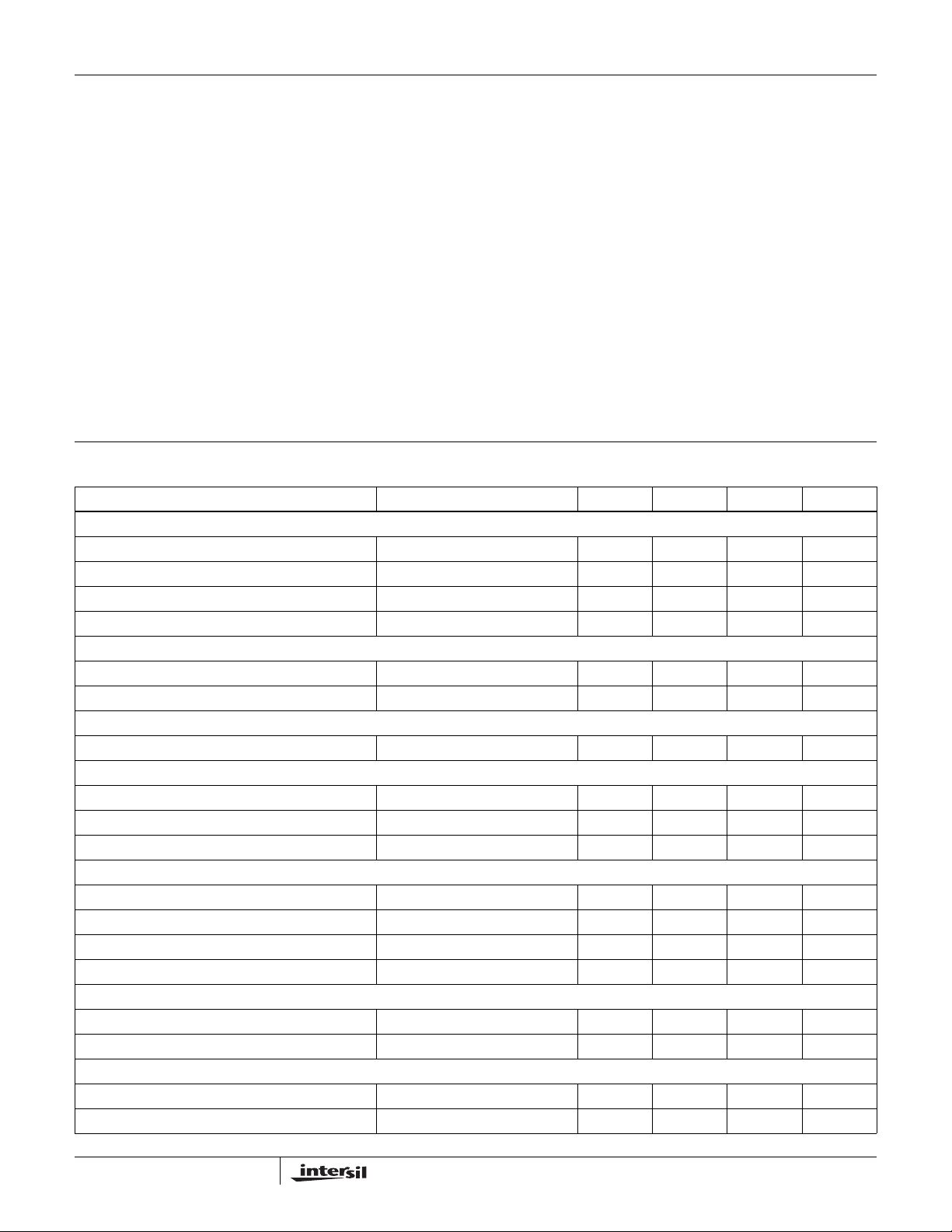
Absolute Maximum Ratings Thermal Information
Supply Voltage, V
PGND to GND . . . . . . . . . . . . . . . . . . . . . . . . . . . . . . . . . . . . . . . . . ±0.3V
Peak GATE Current . . . . . . . . . . . . . . . . . . . . . . . . . . . . . . . . . . . . 1A
ESD Classification . . . . . . . . . . . . . . . . . . . . . Class 1 (HBM, 2500V)
NFB Pin Voltage. . . . . . . . . . . . . . . . . . . . . . ±10V (Transient, 10ms)
CC,PVCC
Operating Conditions
Temperature Range
ISL6401C . . . . . . . . . . . . . . . . . . . . . . . . . . . . . . . . .-40°C to 85°C
Supply Voltage Range (Typical). . . . . . . . . . . . . . . . . . . . . 5V ±10%
CAUTION: Stresses above those listed in “Absolute Maximum Ratings” may cause permanent damage to the device. This is a stress only rating and operation of the
device at these or any other conditions above those indicated in the operational sections of this specification is not implied.
NOTES:
is measured with the component mounted on a high effective thermal conductivity test board in free air. See Tech Brief TB379 for details.
6. θ
JA
7. θ
is measured in free air with the component mounted on a high effective thermal conductivity test board with “direct attach” features. θ
JA
“case temp” is measured at the center of the exposed metal pad on the package underside. See Tech Brief TB379.
8. All voltages are with respect to GND.
Electrical Specifications Recommended operating conditions unless otherwise noted. Refer to Block Diagram and Typical Application
SUPPLY
V
CC
Supply Voltage Range 4.5 5.0 5.5 V
Shutdown Supply Current SHDN = GND - 55 100 µA
Start-Up Current V
Operating Supply Current (Note 10) - 3.7 6.0 mA
REFERENCE VOLTAGE
Output Voltage 1.237 1.25 1.262 V
Long Term Stability T
NEGATIVE FEEDBACK
Source Current -1.02.0mA
CURRENT SENSE
Maximum Input Signal 0.2 0.260 0.3 V
Input Bias Current -2.0 0.0 2.0 µA
Overcurrent Threshold 0.4 0.52 0.6 V
ERROR AMPLIFIER
Open Loop Voltage Gain -78-dB
Gain-Bandwidth Product 10 - - MHz
Input Voltage 1.225 1.25 1.275 V
Input Bias Current -1.0-µA
PWM
Maximum Duty Cycle 47 48 50 %
Minimum Duty Cycle COMP = 0V - 0 - %
UNDERVOLTAGE LOCKOUT
Start Threshold 3.7 4.1 4.3 V
Stop Threshold 3.2 3.6 4.0 V
. . . . . . . . . . . . . . . . GND -0.3V to +7.0V
schematic. V
PARAMETER TEST CONDITIONS MIN TYP MAX UNITS
= +5.0V ±10%, TA = -40 to 85°C (Note 9), Typical values are at TA = 25°C
CC
< 3.7V - 0.1 0.20 mA
CC
= 125°C, 1000 hours - 5 - mV
A
Thermal Resistance (Typical) θ
14 Lead SOIC (Note 6) . . . . . . . . . . . . 90 NA
16 Lead QFN (Note 7) . . . . . . . . . . . . . 46 9
Maximum Junction Temperature (Plastic Package) . -55°C to 150°C
Maximum Storage Temperature Range. . . . . . . . . . . -65°C to 150°C
Maximum Lead Temperature (Soldering 10s) . . . . . . . . . . . . . 300°C
(SOIC - Lead Tips Only)
For Recommended soldering conditions see Tech Brief TB389.
(°C/W) θJC (°C/W)
JA
JC,
the
3
FN9007.7
April 13, 2005
Page 4
ISL6401
www.BDTIC.com/Intersil
Electrical Specifications Recommended operating conditions unless otherwise noted. Refer to Block Diagram and Typical Application
schematic. V
PARAMETER TEST CONDITIONS MIN TYP MAX UNITS
Start to Stop Hysteresis 0.2 0.5 0.8 V
SOFT-START - DIGITAL
COMP Rise Time Rise from 0.5V to REF -1V - 2048 clk -
OSCILLATOR
Gate Output Frequency Ct = 560pF 90 100 108 kHz
Gate Output Frequency Range 50 - 600 kHz
Temperature Stability -5-%
Sync. Frequency Range 1.1 Times the natural switching
Sync Input HIGH 3.5 - - V
Sync Input LOW --1.5V
Minimum Sync. Input Pulse Duty Cycle - 20 - %
OUTPUT
GATE Low Level -0.20.5V
GATE High V
Rise Time C load = 1500pF - 35 - ns
Fall Time C load = 1500pF - 40 - ns
NOTES:
9. Specifications at -40°C are guaranteed by design, not production tested.
10. This is the V
SAT
current consumed when the device is active but not switching. Does not include gate drive current.
CC
= +5.0V ±10%, TA = -40 to 85°C (Note 9), Typical values are at TA = 25°C (Continued)
CC
frequency.
--1.2MHz
4.4 4.9 5.5 V
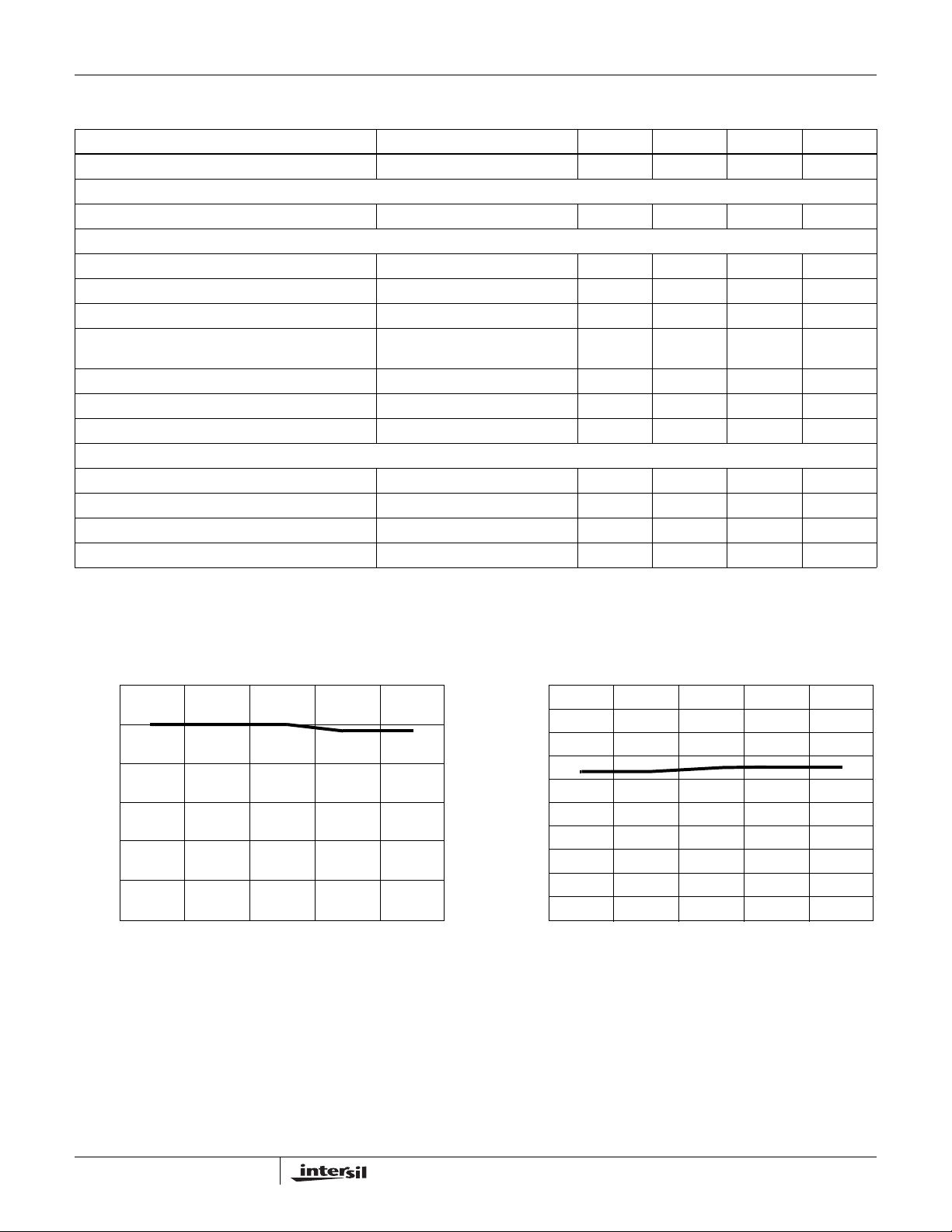
Typical Performance Curves
120
100
80
60
40
FREQUENCY (kHz)
20
0
-40 -20 25 60 85
FIGURE 1. FREQUENCY vs TEMPERATURE FIGURE 2. REFERENCE VOLTAGE vs TEMPERATURE
TEMPERATURE (°C)
VOLTAGE (V)
2.0
1.8
1.6
1.4
1.2
1.0
0.8
0.6
0.4
0.2
0
-40 -20 25 60 85
TEMPERATURE (°C)
4
FN9007.7
April 13, 2005
Page 5

Typical Performance Curves (Continued)
0
www.BDTIC.com/Intersil
ISL6401
5.0
4.5
4.0
3.5
3.0
2.5
2.0
CURRENT (mA)
1.5
1.0
0.5
0
-40 -20 25 60 85
FIGURE 3. SUPPLY CURRENT vs TEMPERATURE FIGURE 4. CAPACITANCE vs FREQUENCY
TEMPERATURE (°C)
Pin Descriptions
SD - This pin is logic level compatible and can be pulled
high, tied to V
on the SD activates shutdown, reducing the part’s supply
current to approximately 55µA.
SYNC - This pin is the input pin for external frequency
synchronization. The switching frequency of the device can
be synchronized by an external clock signal inserted at this
pin. The oscillator timing capacitor, C
if an external clock is used. Program the free-running
frequency to be a minimum of 10% slower than the SYNC
input frequency.
CT - This is the oscillator timing pin. The free-running
frequency can be set by connecting a timing capacitor to this
pin. The oscillator produces a sawtooth waveform with a
programmable frequency range of 100kHz to 1.2MHz.
Figure 4 may be used as a guideline in selecting the
capacitor value required for a given frequency.
COMP - COMP is the output of the error amplifier and input
of the current comparator.
The ISL6401 features built-in full cycle soft-start. Soft-start is
implemented as a clamp on the maximum COMP voltage.
FB - Feedback pin that is used for positive output voltage
sensing. It is the inverting input of the error amplifier. The
non-inverting input of the error amplifier is internally tied to a
reference voltage.
NFB-IN - Negative feedback pin that is used for negative
output voltage sensing. It is connected to the inverting input
of the negative feedback amplifier through a 100K source
resistor.
NFB OUT - This pin is the output of the negative feedback
inverter. This pin should be connected the FB pin with a 10K
or left open for normal operation. Logic low
IN
, is still required, even
T
600
500
400
300
200
FREQUENCY (kHz)
100
0
82 120 180 250
300 390 510 610 820 120
CAPACITANCE (pF)
series resistor for negative output voltage regulation
applications.
CS - This is the input of the current sense comparator. The
IC has two different comparators: The PWM comparator and
an overcurrent comparator.
The overcurrent comparator is only intended for fault
sensing, and exceeding the overcurrent threshold will cause
a soft-start cycle.
GND - GND is a small signal reference ground for all analog
functions on this part.
PGND - This pin provides a dedicated ground for the output
gate driver. The GND and PGND pins should be connected
externally using a short printed circuit board trace close to
the IC. This is imperative to prevent large, high frequency
switching currents flowing through the ground metallization
inside the IC. (Decouple PV
to PGND with a low ESR
CC
0.1µF capacitor.)
GATE - This is the device output. It is a high current power
driver capable of driving the gate of a power MOSFET with
peak currents exceeding 1.0A. This GATE output is actively
held low when V
is below the UVLO threshold (3.7V typ).
CC
The high-current power driver consists of FET output
devices, which can switch all the way to GND and all the way
to V
. The output stage also provides very low impedance
CC
to overshoot and undershoot.
PV
- This pin is for separate collector supply to the output
CC
gate drive. Separate PV
and PGnd helps decouple the
CC
IC’s analog circuitry from the high power gate drive noise.
Connect this pin to V
with external short trace on printed
CC
circuit board.
V
- VCC is the power connection for the device. Although
CC
quiescent V
current is very low, total supply current will be
CC
5
FN9007.7
April 13, 2005
Page 6

ISL6401
www.BDTIC.com/Intersil
higher, depending on the output current. Total VCC current is
the sum of the quiescent V
output current. Knowing the operating frequency and the
MOSFET gate charge (Qg), average output current can be
calculated from:
I
To prevent noise problems, bypass V
ceramic capacitor as close to the V
electrolytic capacitor may also be used in addition to the
ceramic capacitor.
OUT
Qg F×=
current and the average
CC
to GND with a
CC
pin as possible. An
CC
Functional Description
Features
The ISL6401 current mode, synchronizable PWM, makes an
ideal choice for low-cost, low-power, multi-output flyback
topology applications with low input-output ripple current
requirements. When configured in a multi-winding flyback
topology, the IC is capable of generating the negative Talk
and Ring voltages required for Ringing Subscriber Line
Interface (RSLIC) power supplies. This approach provides
dual outputs from a single power switch and control IC. Low
current sense voltage and shutdown mode leads to high
efficiency operation. Other features include peak current
mode control, internal soft-start, adjustable current limit,
adjustable frequency and external frequency
synchronization.
Oscillator
The ISL6401 has an internal sawtooth oscillator with a
programmable frequency range of 100kHz to 1MHz, which
can be programmed with a capacitor on the CT pin. (Please
refer to Figure 4 for the capacitance required for a given
frequency.) With a maximum 50% duty cycle operation, the
output switching frequency is half the oscillator frequency.
Implementing Synchronization
The oscillator can be synchronized by an external clock
inserted at the SYNC pin. Program the free running
frequency of the oscillator to be 10% slower than the desired
synchronous frequency. The external clock signal should
have a minimum pulse width of 20ns.
Soft-Start Operation
The ISL6401 features an internal digital soft-start with no
external capacitor required. Soft-start is used to reduce
transformer and output capacitor stress and to reduce the
surge on the input circuits, when the converter action starts.
The considerable capacitance on the output lines should be
charged slowly, so as not to reflect an excessive transient. A
very wide initial pulse could result in saturation of the core
and voltage overshoot on the output, if the inductor current is
allowed to rise to a high value during start-up.
Upon start-up, the peak primary current increments from
1/5th of the value set by R
steps, over 2048 cycles of Fosc or Fsync. Soft-start clamps
to the full current limit value in
CS
the error amplifier output (COMP pin) and the reference
input (non-inverting terminal of the error amplifier) to the
internally generated soft-start voltage. The oscillator
sawtooth waveform is compared to the ramping error
amplifier voltage. This generates GATE pulses of increasing
width that charge the output capacitor(s). With sufficient
output voltage, the clamp on the reference input controls the
output voltage. When the internally generated soft-start
voltage exceeds the FB pin voltage, the output voltage is in
regulation. This method provides a rapid, controlled output
voltage rise. Soft-start is implemented during start-up, after
an overcurrent has cleared, or when exiting shutdown or
undervoltage lock-out (UVLO).
Gate Drive
The ISL6401 is capable of sourcing 1A of peak-drive current.
Separate collector supply (PV
pins help isolate the IC’s analog circuitry from the high power
gate drive noise. To limit the peak current through the IC, an
external resistor is placed between the totem-pole output of
the IC and the gate of the MOSFET. The minimum value of
this resistor is determined by:
Rgate = (Vdd(min) - Vsat) / Igate(peak)
This small series resistor also damps any oscillations
caused by the resonant tank of the parasitic inductances in
the traces of the board and the FET’s input capacitance. A
pull-down resistor is sometimes added to the gate drive to
insure the MOSFET gate does not get charged to its turn-on
threshold during device start-up. Adding a fast-switching
diode and smaller value resistor in parallel with the gate
resistor helps to control the current the IC needs to sink
during turn-off and protects the output stage of the device.
These components also help to reduce turn-off losses, which
tend to dominate the switching losses in discontinuous
current-mode (DCM) converters.
) and power ground (PGnd)
CC
Ground Plane Requirements
Careful layout is essential for correct operation of the device.
A good ground plane must be employed. A unique section of
the ground plane must be designated for high di/dt currents
associated with the output stage. Power ground (PGND) can
be separated from the analog ground (GND) and connected
at a single point. V
with good high frequency capacitors. The return connection
for input power to the system and the bulk input capacitor
should be connected to the PGND ground plane.
should be bypassed directly to PGND
CC
Application Information
Subscriber Line Interface Circuit Requirements
As worldwide demand for inexpensive Voice over Internet
Protocol telephony grows, so will the need for ICs that
enable compatibility between new telephony systems and
older telephones based on analog standards. Old style
telephones require signal and power inputs that are not
generally available on purely digital systems. Analog ring
6
FN9007.7
April 13, 2005
Page 7

ISL6401
www.BDTIC.com/Intersil
signal generation and off-hook loop current supply are two
analog functions that are performed by Subscriber Line
Interface Circuits (SLICs). A SLIC is the primary interface
between the 4-wire (ground referenced) low voltage switch
environment and the 2 wire (floating) high voltage loop
environment. It performs a number of important functions
including battery feed, overvoltage protection, ringing,
signaling, coding, hybrid balancing and testing.
The Ringing SLIC (RSLIC) typically requires two high
voltage power supply inputs. The first is a tightly regulated
voltage around -24V or -48V for off-hook voice transmission.
The second is a loosely regulated -70 to -100V for ring tone
generation. When the switch hook is released the phone
puts approximately 200Ω of resistance across the phone
terminals. Once voice transmission begins, the SLIC
requires a lower voltage input to establish a current loop of
approximately 25mA. The loop feeds the 200Ω, protection
resistors, and line resistances within the phone.
ISL6401 Flyback Reference Design
The Typical Application Schematic shows a current mode
power supply using the Intersil ISL6401 in a standard
flyback topology. The IC requires +5V Bias. The application
circuit is intended for wall adapters that power home
gateway/router boxes. This circuit input voltage can be 9V
to 20V with the selected transformer and external
components.
The output voltages are -24V at 120mA and -72V at
120mA. The circuit uses inexpensive transformers to
generate both outputs using a single controller. The
transformer turns ratio is such that 24V appear across each
secondary winding and the primary during the switch offtime. The remaining secondary windings are stacked in
series to develop -48V. The -48V section is then stacked on
the -24V section to get the -72V. This technique provides
good cross regulation, lowers the voltage rating required
for the output capacitors, and lowers the RMS current,
allowing the use of less expensive output capacitors. Also,
the selection of a transformer with multifilar winding lowers
the leakage inductance and cost. The -24V output is
precisely regulated by feeding back this output to the
controller. The -72V output is derived from the third pair of
windings. Regulation of this output is obtained by the turn’s
ratio of the transformer with -24V output, as well as with
split feedback.
Circuit Element Descriptions
• Transformers T1, MOSFET Q1, Schottky diode D1, D2,
and input capacitor C1 and C2 form the power stage of
the converter. Power resistor R5 senses the switch
current and converts this current into a voltage to be
sensed by the primary side controller feedback
comparator.
• Capacitors C9 to C12 filter out high frequency noise on the
output bus directly at the output diode.
• R7 and C8 provide secondary side snubbing.
• R6 and C7 filter out the leading edge voltage spikes
resulting from the leakage inductance of the transformer.
• C4 sets the switching frequency of the converter.
• C3 is a decoupling capacitor, which should always be a
good quality low-ESR/ESL type capacitor, placed as close
to the IC pins as possible and returned directly to the IC
ground reference.
• The gate drive circuitry can be composed of a small gate
drive resistor, necessary for damping any oscillations
resulting from the input capacitance of Q1 and any
parasitic stray inductance.
• The voltage sense feedback loop is comprised of R4 and
R3. Feedback components R1, C6, and C5 provide the
necessary gain and pole to stabilize the control loop.
Component Selection Guidelines
Power MOSFET
The MOSFET switch is selected to meet the drain to source
voltage stress resulting from the maximum input voltage
(V
output voltage (V
(V
assumed to be 30% of the input voltage.
Vds (stress) = [(V
The switch must also be able to conduct the repetitive peak
primary current as determined by:
Ipeak (primary) = (Vin
The primary current waveform of a discontinuous mode
flyback converter is triangular in shape, therefore, its root
mean square(rms) current is calculated by:
Irms prim()IPEAKprim 3⁄()TONmax()T⁄()=
The chosen device should also have a low R
because the conduction losses of the device are proportional
to the square of the primary rms current through the device.
Selection of a device that has a peak current rating of at
least three times the peak current usually insures acceptably
low conduction losses.
Pconduction = (I
), the reflected secondary voltages, equal to the
IN(max)
), and the voltage spike due to the leakage inductance,
F
), plus the output diode voltage drop
OUT
) + (N)(Vout +Vf)] + (0.3)(V
IN(max)
prms
2
min
) (R
- Vds) (t
DS(on)
ON(max)
)
) / Lp
DS(ON)
IN(max)
value,
)
7
FN9007.7
April 13, 2005
Page 8

ISL6401
www.BDTIC.com/Intersil
Switching losses are the result of overlapping drain current
and source voltage at turn-off. The drain voltage begins to
rise only after the miller capacitance of the device begins to
discharge. This discharging time is a function of the external
gate resistance, Rgate and the gate-to-drain miller charge
Qgd, as shown in the following equation,
T miller = (Qgd)(R
GATE
)/(Vdd-Vth),
where Vth is the turn ON threshold voltage of the gate.
The power loss due to the external capacitance of the
MOSFET also contributes to the total switching losses,
which can be calculated as shown.
C
ossVDS stress()
P
switchingFsw
I
++
peak primary()tmiller
-------------------------------------------------------- V
=
2
2×
+
DS stress()
During turn on there is no overlap of drain voltage and
current because there is no current in a discontinuous
current mode converter at turn-on. Minimal losses also occur
during the off-time of the FET due to the leakage current.
P
off (time)
= (1 - D
max
)(I
leak
)(V
ds(stress)
)
Output and Input Capacitors
Output capacitors are selected based upon their value,
equivalent series resistance (ESR), equivalent series
inductance and capacitor ripple current rating. The capacitor
value controls the peak-to-peak output ripple voltage at the
switching frequency. Assuming a linear decay of the
capacitor voltage during the off time, during which the
capacitor must supply the load current, the minimum value of
the output capacitor can be calculated as follows,
Cout = [(T- T
ON(max)
where Vripple is the acceptable peak-to peak output voltage
ripple. However, there are practical limitations to how low a
single stage output filter can reduce the ripple voltage and
sometimes an extra LC filter stage is necessary. This second
stage filter would also reduce the output high frequency noise.
Parasitic resistance and inductance in the output capacitors
tend to make the ripple voltage much greater than expected,
based upon the above equation. Using capacitors with the
lowest possible ESR and ESL helps reduce high frequency
ripple. The rms ripple current that the output capacitors
experience is not the same as the secondary side rms output
current; it is the AC portion of it. The secondary side rms
current is in the shape of a clipped sawtooth, or trapezoid,
where the output capacitor’s current waveform is in the shape
of right triangle. Therefore, the typical capacitor ripple current
rating the output capacitor must meet is equal to,
)(Iout)] / Vripple),
where Ipeak (sec) is the peak-secondary current and t
RESET
is equal to the off-time of the switch. The same selection
criteria is used for the input capacitor, keeping in mind these
capacitors must also be rated to handle the maximum input
voltage.
Output Voltage
The output voltage can be set by a feedback resistor divider
network. The output is resistively divided and compared to
the reference voltage. For negative flyback output
applications, the sensed output will be fed to the NFB IN pin.
The sensed voltage in inverted, and this positive voltage is
fed to the FB- inverting input pin of the error amplifier. The
non-inverting input of the error amplifier will be a reference
voltage. So, when FB- is higher than REF voltage, the output
drivers are turned off. The opposite happens when the
resistively divided output voltage falls below the 1.24V
reference voltage.
Output Diode
The output diode in a flyback converter is subject to large
peak and rms current stresses. Schottky diodes are
recommended, because of their low forward-voltage drop and
the virtual absence of minority carrier reverse recovery. The
secondary-side Schottky rectifier was selected to meet the
working peak-reverse voltage, the peak repetitive forwardcurrent and the average forward-current of the application.
The working peak-reverse voltage Vrev, or blocking voltage, is
calculated according to the following equation:
V
= [(V
R
INmax
+ V
RDSon
) / N ]+ V
OUT
The reflected peak primary current constitutes the peak
repetitive forward-current through the diode. Because all
current to the output capacitors and load must flow through
the diode, the average forward diode current is equal to the
steady-state load current. Power loss in the Schottky is the
sum of the conduction losses and reverse leakage losses.
Conduction losses are calculated using the forward voltage
drop across the diode and the average forward-current.
Reverse leakage losses are dependent upon the reverse
leakage-current, the blocking voltage, and the on-time of
the FET.
Determining the Turns Ratio of the Flyback
Transformer
The turns ratio of the flyback transformer can be calculated
by using the this steady-state volt-second approach:
n = [(V
INmin
- VDS)(D
max
)(T)] / [(V
+ VF)(0.8 - D
OUT
max
)(T)]
3()Treset()
4
--------------------------------–
Treset
Irms Ipeak()
=
------------------ -
-----------------------------------------------
T
T
12
8
FN9007.7
April 13, 2005
Page 9

ISL6401
www.BDTIC.com/Intersil
Primary Inductance
The flyback transformer is actually a coupled inductor, acting
as an energy storage unit, as well as performing the usual
transformer functions. Crucial considerations include primary
inductance, working flux density swing, gap length, the
winding scheme and wire diameter. The primary inductance,
LP, for a discontinuous mode flyback converter can be
calculated according to the following relationship:
Lp = n [(V
Where n is the assumed efficiency of the converter and Iout
is the output current. The ferrite core should have high
saturation, low residual flux density, and low losses. An
EFD15 core material proved to be suitable for this
application.
INmin
- VDS)(T
ONmax
)]2 / (2)(T)(V
OUT
)(I
OUT
)
Current Sense
The ground referenced sense resistor is selected such that
the maximum peak primary current trips the CS pin threshold
when this current is 10% higher than its normal operating
peak value at the minimum input voltage.
This limits the peak primary current in the event of an output
short circuit. This resistor must have a power rating to meet
2
the (I
square (rms) primary current. Because this resistor defines
the maximum peak primary current, the input energy to the
transformer is defined and equal to (L
defined energy in a fixed frequency discontinuous-mode
flyback results in a fixed output power.
The advantage of current-mode control is that the output
voltage is held constant despite changes in the input voltage,
because the peak-primary current remains constant; the
slope of this inductor current and its pulse width are
adjusted. Leading edge spikes or noise are caused by the
reverse recovery of the rectifier, equivalent capacitive
loading on the secondary, and parasitic circuit inductances.
A small low pass RC filter is added to the current-sense
signal to filter out these spikes, so the comparator does not
assume an overload condition is present during switch turnon. To avoid excessive phase lag on the current-sense
signal, the low pass filter corner frequency is selected to be
at least a decade above the switching frequency.
)(R) requirement, where I
rms
is the root mean
rms
2
)(I
PEAK
P
) / 2. This
9
FN9007.7
April 13, 2005
Page 10

Small Outline Plastic Packages (SOIC)
www.BDTIC.com/Intersil
ISL6401
N
INDEX
AREA
123
-AD
e
B
0.25(0.010) C AM BS
NOTES:
1. Symbols are defined in the “MO Series Symbol List” in Section 2.2 of
Publication Number 95.
2. Dimensioning and tolerancing per ANSI Y14.5M-1982.
3. Dimension “D” does not include mold flash, protrusions or gate burrs.
Mold flash, protrusion and gate burrs shall not exceed 0.15mm (0.006
inch) per side.
4. Dimension “E” does not include interlead flash or protrusions. Interlead
flash and protrusions shall not exceed 0.25mm (0.010 inch) per side.
5. The chamfer on the body is optional. If it is not present, a visual index
feature must be located within the crosshatched area.
6. “L” is the length of terminal for soldering to a substrate.
7. “N” is the number of terminal positions.
8. Terminal numbers are shown for reference only.
9. The lead width “B”, as measured 0.36mm (0.014 inch) or greater
above the seating plane, shall not exceed a maximum value of
0.61mm (0.024 inch).
10. Controlling dimension: MILLIMETER. Converted inch dimensions
are not necessarily exact.
E
-B-
SEATING PLANE
A
-C-
M
0.25(0.010) BM M
H
α
µ
A1
0.10(0.004)
L
h x 45
o
C
M14.15 (JEDEC MS-012-AB ISSUE C)
14 LEAD NARROW BODY SMALL OUTLINE PLASTIC
PACKAGE
INCHES MILLIMETERS
SYMBOL
A 0.0532 0.0688 1.35 1.75 -
A1 0.0040 0.0098 0.10 0.25 -
B 0.013 0.020 0.33 0.51 9
C 0.0075 0.0098 0.19 0.25 -
D 0.3367 0.3444 8.55 8.75 3
E 0.1497 0.1574 3.80 4.00 4
e 0.050 BSC 1.27 BSC -
H 0.2284 0.2440 5.80 6.20 -
h 0.0099 0.0196 0.25 0.50 5
L 0.016 0.050 0.40 1.27 6
N14 147
o
α
0
o
8
o
0
o
8
Rev. 0 12/93
NOTESMIN MAX MIN MAX
-
10
FN9007.7
April 13, 2005
Page 11

ISL6401
www.BDTIC.com/Intersil
Quad Flat No-Lead Plastic Package (QFN)
Micro Lead Frame Plastic Package (MLFP)
L16.4x4
16 LEAD QUAD FLAT NO-LEAD PLASTIC PACKAGE
(COMPLIANT TO JEDEC MO-220-VGGC ISSUE C)
MILLIMETERS
SYMBOL
A 0.80 0.90 1.00 -
A1 - - 0.05 -
A2 - - 1.00 9
A3 0.20 REF 9
b 0.23 0.28 0.35 5, 8
D 4.00 BSC -
D1 3.75 BSC 9
D2 1.95 2.10 2.25 7, 8
E 4.00 BSC -
E1 3.75 BSC 9
E2 1.95 2.10 2.25 7, 8
e 0.65 BSC -
k0.25 - - -
L 0.50 0.60 0.75 8
L1 - - 0.15 10
N162
Nd 4 3
Ne 4 3
P- -0.609
θ --129
NOTES:
1. Dimensioning and tolerancing conform to ASME Y14.5-1994.
2. N is the number of terminals.
3. Nd and Ne refer to the number of terminals on each D and E.
4. All dimensions are in millimeters. Angles are in degrees.
5. Dimension b applies to the metallized terminal and is measured
between 0.15mm and 0.30mm from the terminal tip.
6. The configuration of the pin #1 identifier is optional, but must be
located within the zone indicated. The pin #1 identifier may be
either a mold or mark feature.
7. Dimensions D2 and E2 are for the exposed pads which provide
improved electrical and thermal performance.
8. Nominal dimensions are provided to assist with PCB Land Pattern
Design efforts, see Intersil Technical Brief TB389.
9. Features and dimensions A2, A3, D1, E1, P & θ are present when
Anvil singulation method is used and not present for saw
singulation.
10. Depending on the method of lead termination at the edge of the
package, a maximum 0.15mm pull back (L1) maybe present. L
minus L1 to be equal to or greater than 0.3mm.
NOTESMIN NOMINAL MAX
Rev. 5 5/04
All Intersil U.S. products are manufactured, assembled and tested utilizing ISO9000 quality systems.
Intersil Corporation’s quality certifications can be viewed at www.intersil.com/design/quality
Intersil products are sold by description only. Intersil Corporation reserves the right to make changes in circuit design, software and/or specifications at any time without
notice. Accordingly, the reader is cautioned to verify that data sheets are current before placing orders. Information furnished by Intersil is believed to be accurate and
reliable. However, no responsibility is assumed by Intersil or its subsidiaries for its use; nor for any infringements of patents or other rights of third parties which may result
from its use. No license is granted by implication or otherwise under any patent or patent rights of Intersil or its subsidiaries.
For information regarding Intersil Corporation and its products, see www.intersil.com
11
FN9007.7
April 13, 2005
 Loading...