®
ISL6323
Hybrid SVI/PVI
Data Sheet
Monolithic Dual PWM Hybrid Controller
Powering AMD SVI Split-Plane and PVI
Uniplane Processors
The ISL6323 dual PWM controller delivers high efficiency
and tight regulation from two synchronous buck DC/DC
converters. The ISL6323 supports hybrid power control of
AMD processors which operate from either a 6-bit parallel
VID interface (PVI) or a serial VID interface (SVI). The dual
output ISL6323 features a multiphase controller to support
uniplane VDD core voltage and a single phase controller to
power the Northbridge (VDDNB) in SVI mode. Only the
multiphase controller is active in PVI mode to support
uniplane VDD only processors.
A precision uniplane core voltage regulation system is
provided by a 2- to 4-phase PWM voltage regulator (VR)
controller. The integration of two power MOSFET drivers,
adding flexibility in layout, reduce the number of external
components in the multiphase section. A single phase PWM
controller with integrated driver provides a second precision
voltage regulation system for the North Bridge portion of the
processor. This monolithic, dual controller with integrated
driver solution provides a cost and space saving power
management solution.
For applications which benefit from load line programming to
reduce bulk output capacitors, the ISL6323 features output
voltage droop. The multiphase portion also in cludes advanced
control loop features for optimal transient response to load
application and removal. One of these features is highly
accurate, fully differential, continuous DCR current sensing for
load line programming and channel current balance. Dual
edge modulation is another unique feature, allowing for
quicker initial response to high di/dt load transients.
Ordering Information
PART
NUMBER
(Note)
ISL6323CRZ* ISL6323 CRZ 0 to +70 48 Ld 7x7 QFN L48.7x7
ISL6323IRZ* ISL6323 IRZ -40 to +85 48 Ld 7x7 QFN L48.7x7
*Add “-T” suffix for tape and reel. Please refer to TB347 for details on
reel specifications.
NOTE: These Intersil Pb-free plastic packaged products employ
special Pb-free material sets, molding compounds/die attach
materials, and 100% matte tin plate plus anneal (e3 termination
finish, which is RoHS compliant and compatible with both SnPb and
Pb-free soldering operations). Intersil Pb-free products are MSL
classified at Pb-free peak reflow temperatures that meet or exceed
the Pb-free requirements of IPC/JEDEC J STD-020.
PART
MARKING
TEMP.
(°C)
PACKAGE
(Pb-free)
PKG.
DWG. #
October 21, 2008
FN9278.4
Features
• Processor Core Voltage Via Integrated MultiPhase
Power Conversion
• Configuration Flexibility
- 2-Phase Operation with Internal Drivers
- 3- or 4-Phase Operation with External PWM Drivers
• Serial VID Interface Inputs
- Two Wire, Clock and Data, Bus
- Conforms to AMD SVI Specifications
• Parallel VID Interface Inputs
- 6-bit VID input
- 0.775V to 1.55V in 25mV Steps
- 0.375V to 0.7625V in 12.5mV Steps
• Precision Core Voltage Regulation
- Differential Remote Voltage Sensing
- ±0.5% System Accuracy Over-Temperature
- Adjustable Reference-Voltage Offset
• Optimal Processor Core Voltage Transient Response
- Adaptive Phase Alignment (APA)
- Active Pulse Positioning Modulation
• Fully Differential, Continuous DCR Current Sensing
- Accurate Load Line Programming
- Precision Channel Current Balancing
• Variable Gate Drive Bias: 5V to 12V
• Overcurrent Protection
• Multi-tiered Overvoltage Protection
• Selectable Switching Frequency up to 1MHz
• Simultaneous Digital Soft-Start of Both Outputs
• Processor NorthBridge Voltage Via Single Phase
Power Conversion
• Precision Voltage Regulation
- Differential Remote Voltage Sensing
- ±0.5% System Accuracy Over-Temperature
• Serial VID Interface Inputs
- Two Wire, Clock and Data, Bus
- Conforms to AMD SVI Specifications
• Overcurrent Protection
• Continuous DCR Current Sensing
• Variable Gate Drive Bias: 5V to 12V
• Simultaneous Digital Soft-Start of Both Outputs
• Selectable Switching Frequency up to 1MHz
• Pb-Free (RoHS Compliant)
1
CAUTION: These devices are sensitive to electrostatic discharge; follow proper IC Handling Procedures.
1-888-INTERSIL or 1-888-468-3774
| Intersil (and design) is a registered trademark of Intersil Americas Inc.
Copyright Intersil Americas Inc. 2007, 2008. All Rights Reserved
All other trademarks mentioned are the property of their respective owners.
ISL6323ISL6323
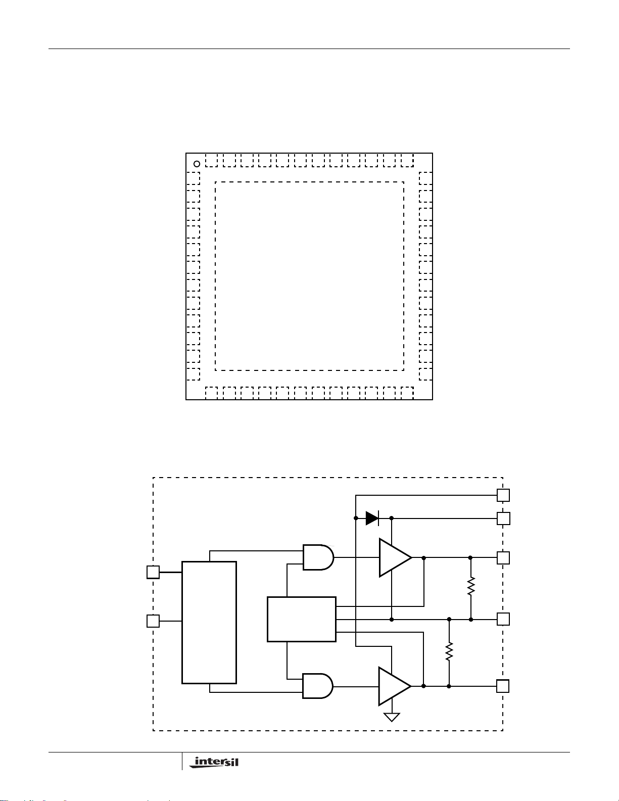
Pinout
FB_NB
ISEN_NB+
RGND_NB
VID0/VFIXEN
VID1/SEL
VID2/SVD
VID3/SVC
VID4
VID5
VCC
FS
RGND
ISL6323
(48 LD QFN)
TOP VIEW
ISEN_NB-
ISEN4+
COMP_NB
48 47 46 45 44 43 42 41 40 39 38 37
1
2
3
4
5
6
7
8
9
10
11
12
13 14 15 16 17 18 19 20 21 22 23 24
ISEN4-
ISEN3-
49
GND
PVCC_NB
LGATE_NB
BOOT_NB
ISEN3+
UGATE_NB
PHASE_NB
VDDPWRGD
PWM4
36
PWM3
35
PWROK
34
PHASE1
33
UGATE1
32
BOOT1
31
LGATE1
30
29
PVCC1_2
28
LGATE2
27
BOOT2
26
UGATE2
25
PHASE2
VSEN
Integrated Driver Block Diagram
PWM
SOFT-START
AND
FAULT LOGIC
GATE
CONTROL
LOGIC
OFS
DVC
FB
RSET
SHOOT-
THROUGH
PROTECTION
COMP
APA
ISEN1-
ISEN1+
ISEN2+
EN
ISEN2-
PVCC
BOOT
UGATE
20kΩ
PHASE
10kΩ
LGATE
2
FN9278.4
October 21, 2008
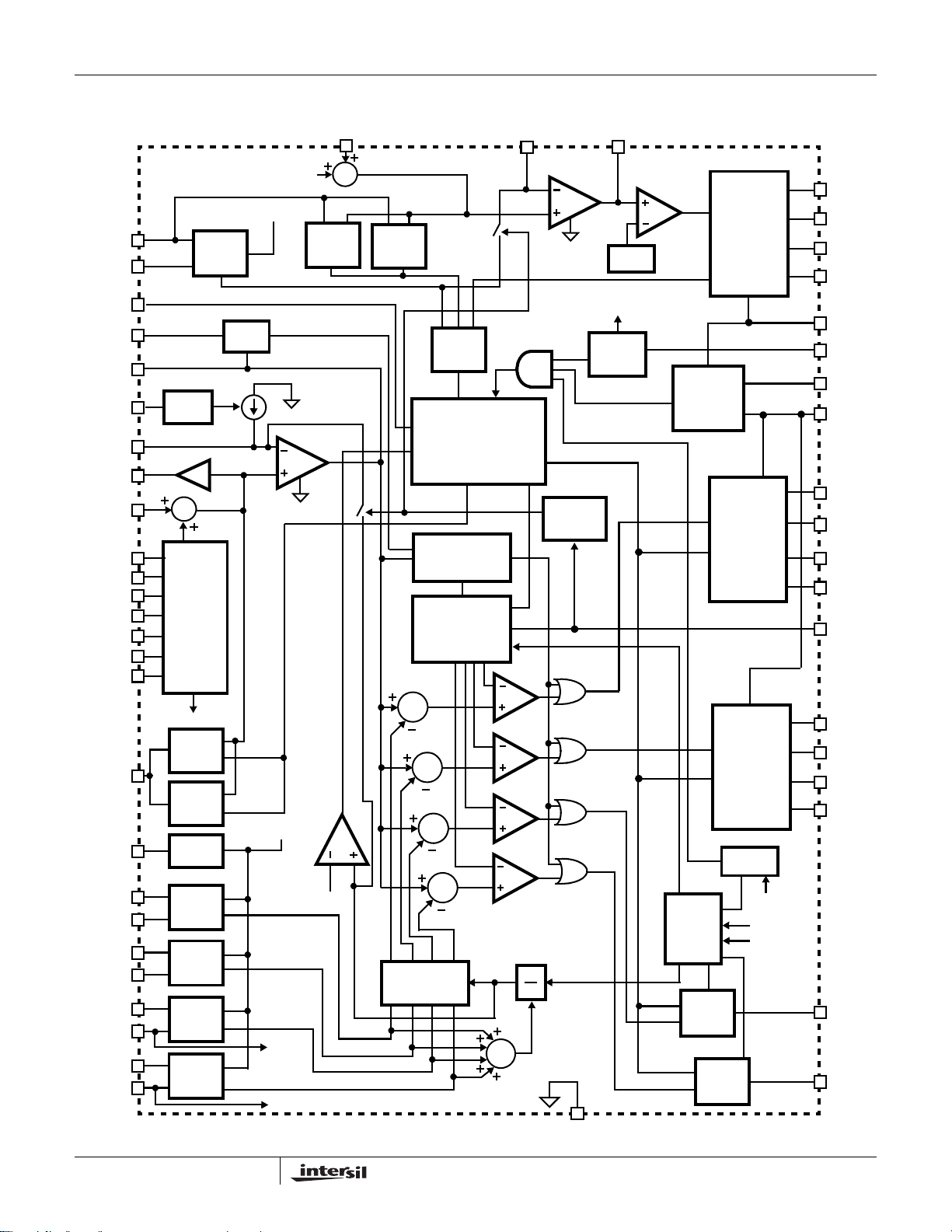
Controller Block Diagram
ISL6323ISL6323
ISEN_NB+
ISEN_NB-
VDDPWRGD
APA
COMP
OFS
FB
DVC
RGND
PWROK
VID0/VFIXEN
VID1/SEL
VID2/SVD
VID3/SVC
VID4
VID5
VSEN
RSET
ISEN1+
ISEN1-
ISEN2+
ISEN2-
ISEN3+
ISEN3-
ISEN4+
ISEN4-
CURRENT
SENSE
OFFSET
2X
∑
SVI
SLAVE
BUS
AND
PVI
DAC
NB_REF
OV
LOGIC
UV
LOGIC
RESISTOR
MATCHING
CH1
CURRENT
SENSE
CH2
CURRENT
SENSE
CH3
CURRENT
SENSE
CH4
CURRENT
SENSE
APA
NB_REF
NB_CS
NB_CS
ISEN3-
ISEN4-
E/A
RGND_NB
UV
LOGIC
OC
I_TRIP
∑
I_AVG
OV
LOGIC
TRIANGLE WAVE
∑
CHANNEL
CURRENT
BALANCE
NB
FAULT
LOGIC
SOFT-START
AND
FAULT LOGIC
LOAD APPL Y
TRANSIENT
ENHANCEMENT
CLOCK AND
GENERATOR
∑
∑
∑
I_AVG
∑
FB_NB
1
N
E/A
DROOP
CONTROL
COMP_NB
RAMP
EN_12V
ENABLE
LOGIC
PWM1
PWM2
PWM3
PWM4
POWER-ON
RESET
CHANNEL
DETECT
PWM3
SIGNAL
LOGIC
SIGNAL
PWM4
LOGIC
MOSFET
DRIVER
MOSFET
DRIVER
MOSFET
DRIVER
PH3/PH4
POR
EN_12V
ISEN3ISEN4-
BOOT_NB
UGATE_NB
PHASE_NB
LGATE_NB
PVCC_NB
EN
VCC
PVCC1_2
BOOT1
UGATE1
PHASE1
LGATE1
FS
BOOT2
UGATE2
PHASE2
LGATE2
PWM3
PWM4
GND
3
FN9278.4
October 21, 2008
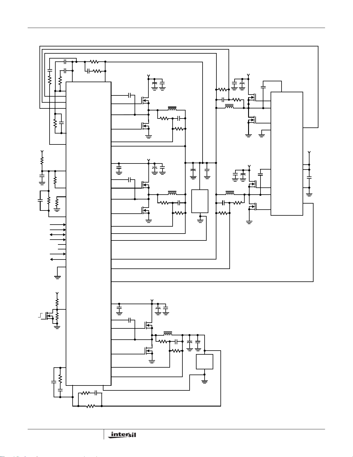
Typical Application - SVI Mode
ISL6323ISL6323
+5V
NC
NC
FB
COMP
ISEN3+
ISEN3PWM3
APA
DVC
VCC
OFS
FS
RSET
VFIXEN
SEL
SVD
SVC
VID4
VID5
PWROK
VDDPWRGD
GND
VSEN
BOOT1
UGATE1
PHASE1
LGATE1
ISEN1-
ISEN1+
PVCC1_2
BOOT2
UGATE2
PHASE2
LGATE2
ISEN2-
ISEN2+
RGND
ISEN4+
ISEN4-
+12V
+12V
VDD
CPU
LOAD
+12V
+12V
BOOT1
UGATE1
PHASE1
LGATE1
PGND
ISL6614
BOOT2
UGATE2
PHASE2
LGATE2
PWM1
VCC
PVCC
GND
PWM2
+12V
OFF
ON
+12V
ISL6323
EN
COMP_NB
FB_NB
PWM4
PVCC_NB
BOOT_NB
UGATE_NB
PHASE_NB
LGATE_NB
ISEN_NB-
ISEN_NB+
RGND_NB
4
+12V
NB
LOAD
VDDNB
FN9278.4
October 21, 2008
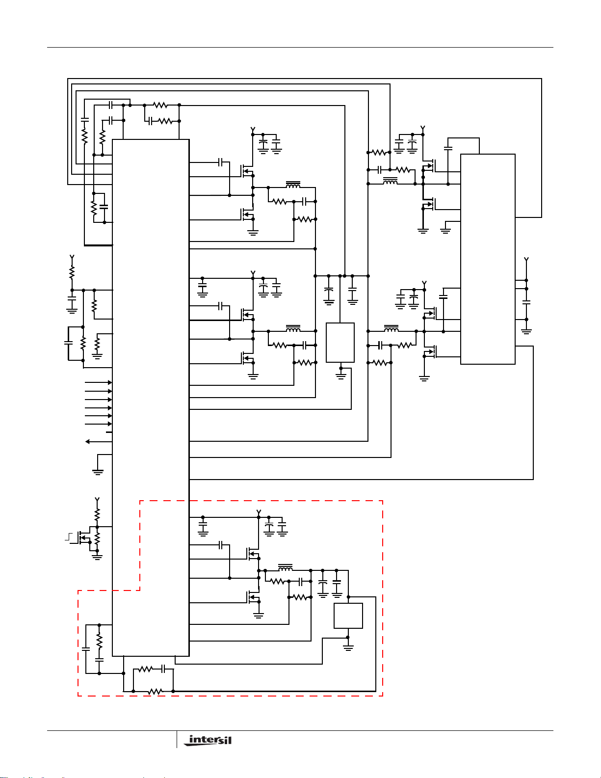
Typical Application - PVI Mode
ISL6323ISL6323
+5V
NC
FB
COMP
ISEN3+
ISEN3PWM3
APA
DVC
VCC
OFS
FS
RSET
VID0
VID1/SEL
VID2
VID3
VID4
VID5
PWROK
VDDPWRGD
GND
VSEN
BOOT1
UGATE1
PHASE1
LGATE1
ISEN1-
ISEN1+
PVCC1_2
BOOT2
UGATE2
PHASE2
LGATE2
ISEN2-
ISEN2+
RGND
ISEN4+
ISEN4-
+12V
+12V
VDD
CPU
LOAD
+12V
+12V
BOOT1
UGATE1
PHASE1
LGATE1
PGND
ISL6614
BOOT2
UGATE2
PHASE2
LGATE2
PWM1
VCC
PVCC
GND
PWM2
+12V
OFF
ON
+12V
ISL6323
EN
COMP_NB
FB_NB
PWM4
PVCC_NB
BOOT_NB
UGATE_NB
PHASE_NB
LGATE_NB
ISEN_NB-
ISEN_NB+
RGND_NB
5
+12V
VDDNB
NB
LOAD
NORTH BRIDGE REGULATOR
DISABLED IN PVI MODE
FN9278.4
October 21, 2008

ISL6323ISL6323
Absolute Maximum Ratings Thermal Information
Supply Voltage (VCC) . . . . . . . . . . . . . . . . . . . . . . . . . .-0.3V to +6V
Supply Voltage (PVCC) . . . . . . . . . . . . . . . . . . . . . . . .-0.3V to +15V
Absolute Boot Voltage (V
Phase Voltage (V
GND - 8V (<400ns, 20µJ) to 24V (<200ns, V
PHASE
Upper Gate Voltage (V
V
- 3.5V (<100ns Pulse Width, 2µJ) to V
Lower Gate Voltage (V
PHASE
). . . . . . . .GND - 0.3V to GND + 36V
BOOT
). . . . . . . . GND - 0.3V to 15V (PVCC = 12)
BOOT
BOOT
= 12V)
+ 0.3V
+ 0.3V
). . . .V
UGATE
LGATE
PHASE
). . . . . . . GND - 0.3V to PVCC + 0.3V
BOOT-PHASE
- 0.3V to V
GND - 5V (<100ns Pulse Width, 2µJ) to PVCC+ 0.3V
Input, Output, or I/O Voltage . . . . . . . . . GND - 0.3V to VCC + 0.3V
CAUTION: Do not operate at or near the maximum ratings listed for extended periods of time. Exposure to such conditions may adversely impact product reliability and
result in failures not covered by warranty.
NOTES:
is measured in free air with the component mounted on a high effective thermal conductivity test board with “direct attach” features. See
1. θ
JA
Tech Brief TB379.
2. For θ
, the “case temp” location is the center of the exposed metal pad on the package underside.
JC
3. Limits should be considered typical and are not production tested.
Electrical Specifications Recommended Operating Conditions (0°C to +70°C), Unless Otherwise Specified. Parameters with MIN and/or
MAX limits are 100% tested at +25°C, unless otherwise specified. Temperature limits established by
characterization and are not production tested.
PARAMETER TEST CONDITIONS MIN TYP MAX UNITS
BIAS SUPPLIES
Input Bias Supply Current I
Gate Drive Bias Current - PVCC1_2 Pin I
Gate Drive Bias Current - PVCC_NB Pin I
VCC POR (Power-On Reset) Threshold VCC Rising 4.20 4.40 4.55 V
PVCC POR (Power-On Reset) Threshold PVCC Rising 4.20 4.40 4.55 V
PWM MODULATOR
Oscillator Frequency Accuracy, f
SW
Typical Adjustment Range of Switching Frequency (Note 3) 0.08 1.0 MHz
Oscillator Ramp Amplitude, V
P-P
CONTROL THRESHOLDS
EN Rising Threshold 0.80 0.88 0.92 V
EN Hysteresis 70 130 190 mV
PWROK Input HIGH Threshold 1.1 V
PWROK Input LOW Threshold 0.95 V
VDDPWRGD Sink Current Open drain, V_VDDPWRGD = 400mV 4 mA
PWM Channel Disable Threshold V
; EN = high 15 22 30 mA
VCC
PVCC1_2
PVCC_NB
; EN = high 1 1.8 3 mA
; EN = high 0.3 0.9 2 mA
VCC Falling 3.70 3.90 4.10 V
PVCC Falling 3.70 3.90 4.10 V
RT = 100kΩ (±0.1%) to Ground, TA = +25°C
(Droop Enabled)
R
= 100kΩ (±0.1%) to VCC, TA = +25°C
T
(Droop Disabled)
(Note 3) 1.50 V
, V
ISEN3-
ISEN4-
Thermal Resistance θ
(°C/W) θJC (°C/W)
JA
QFN Package (Notes 1, 2). . . . . . . . . . 30 2
Maximum Junction Temperature . . . . . . . . . . . . . . . . . . . . . .+150°C
Maximum Storage Temperature Range. . . . . . . . . .-65°C to +150°C
Pb-free reflow profile . . . . . . . . . . . . . . . . . . . . . . . . . .see link below
http://www.intersil.com/pbfree/Pb-FreeReflow.asp
Recommended Operating Conditions
VCC Supply Voltage . . . . . . . . . . . . . . . . . . . . . . . . . . . . . .+5V ±5%
PVCC Supply Voltage . . . . . . . . . . . . . . . . . . . . . . .+5V to 12V ±5%
Ambient Temperature
ISL6323CRZ . . . . . . . . . . . . . . . . . . . . . . . . . . . . . . 0°C to +70°C
ISL6323IRZ . . . . . . . . . . . . . . . . . . . . . . . . . . . . . .-40°C to +85°C
225 250 275 kHz
240 270 300 kHz
4.4 V
6
FN9278.4
October 21, 2008

ISL6323ISL6323
Electrical Specifications Recommended Operating Conditions (0°C to +70°C), Unless Otherwise Specified. Parameters with MIN and/or
MAX limits are 100% tested at +25°C, unless otherwise specified. Temperature limits established by
characterization and are not production tested. (Continued)
PARAMETER TEST CONDITIONS MIN TYP MAX UNITS
PIN_ADJUSTABLE OFFSET
OFS Source Current Accuracy (Positive Offset) R
OFS Sink Current Accuracy (Negative Offset) R
REFERENCE AND DAC
System Accuracy (VDAC > 1.000V) -0.6 0.6 %
System Accuracy (0.600V < VDAC < 1.000V) -1.0 1.0 %
System Accuracy (VDAC < 0.600V) -2.0 2.0 %
DVC Voltage Gain VDAC = 1V 2.0 V
APA Current Tolerance V
ERROR AMPLIFIER
DC Gain R
Gain-Bandwidth Product (Note 3) C
Slew Rate (Note 3) C
Maximum Output Voltage Load = 1mA 3.80 4.20 V
Minimum Output Voltage Load = -1mA 1.3 1.6 V
SOFT-START RAMP
Soft-Start Ramp Rate 2.2 3.0 4.0 mV/µs
PWM OUTPUTS
PWM Output Voltage LOW Threshold I
PWM Output Voltage HIGH Threshold I
CURRENT SENSING - CORE CONTROLLER
Current Sense Resistance, R
ISEN
(Internal)
(Note 3)
Average Sensed and Droop Current Tolerance ISEN1+ = ISEN2+ = ISEN3+ = ISEN4+ = 77µA 68 77 87 µA
CURRENT SENSING - NB CONTROLLER
Current Sense Resistance, R
(Note 3)
ISEN_NB
(Internal)
Sensed Current Tolerance ISEN_NB = 80µA 80 µA
OVERCURRENT PROTECTION
Overcurrent Trip Level - Average Channel Normal Operation 83 100 111 µA
Overcurrent Trip Level - Individual Channel Normal Operation 142 µA
POWER GOOD
Overvoltage Threshold VSEN Rising (Core and North Bridge) VDAC
Undervoltage Threshold VSEN Falling (Core) VDAC -
Power Good Hysteresis 50 mV
= 10kΩ (±0.1%) from OFS to GND 27.5 31 34.5 µA
OFS
= 30kΩ (±0.1%) from OFS to VCC 50.5 53.5 56.5 µA
OFS
= 1V 90 100 108 µA
APA
= 10k to ground, (Note 3) 96 dB
L
= 100pF, RL = 10k to ground, (Note 3) 20 MHz
L
= 100pF, Load = ±400µA, (Note 3) 8 V/µs
L
= ±500µA 0.5 V
LOAD
= ±500μA4.5V
LOAD
TA = +25°C 2400 Ω
TA = +25°C 2400 Ω
Dynamic VID Change (Note 3) 130 µA
Dynamic VID Change (Note 3) 190 µA
+225mV
325mV
VSEN Falling (North Bridge) VDAC -
310mV
VDAC +
250mV
VDAC -
300mV
VDAC -
275mV
VDAC +
275mV
VDAC -
275mV
VDAC -
245mV
V
mV
mV
7
FN9278.4
October 21, 2008
ISL6323ISL6323
Electrical Specifications Recommended Operating Conditions (0°C to +70°C), Unless Otherwise Specified. Parameters with MIN and/or
MAX limits are 100% tested at +25°C, unless otherwise specified. Temperature limits established by
characterization and are not production tested. (Continued)
PARAMETER TEST CONDITIONS MIN TYP MAX UNITS
OVERVOLTAGE PROTECTION
OVP Trip Level 1.73 1.80 1.84 V
OVP Lower Gate Release Threshold 350 400 mV
SWITCHING TIME (Note 3) [See “Timing Diagram” on page 8]
UGATE Rise Time t
LGATE Rise Time t
UGATE Fall Time t
LGATE Fall Time t
UGATE Turn-On Non-overlap t
LGATE Turn-On Non-overlap t
RUGATE; VPVCC
RLGATE; VPVCC
FUGATE; VPVCC
FLGATE; VPVCC
PDHUGATE
PDHLGATE
GATE DRIVE RESISTANCE (Note 3)
Upper Drive Source Resistance V
Upper Drive Sink Resistance V
Lower Drive Source Resistance V
Lower Drive Sink Resistance V
= 12V, 15mA Source Current 2.0 Ω
PVCC
= 12V, 15mA Sink Current 1.65 Ω
PVCC
= 12V, 15mA Source Current 1.25 Ω
PVCC
= 12V, 15mA Sink Current 0.80 Ω
PVCC
MODE SELECTION
VID1/SEL Input Low EN taken from HI to LO, VDDIO = 1.5V 0.45 V
VID1/SEL Input High EN taken from LO to HI, VDDIO = 1.5V 1.00 V
PVI INTERFACE
VIDx Pull-down VDDIO = 1.5V 30 45 µA
VIDx Input Low VDDIO = 1.5V 0.45 V
VIDx Input High VDDIO = 1.5V 1.00 V
SVI INTERFACE
SVC, SVD Input LOW (VIL) 0.4 V
SVC, SVD Input HIGH (VIH) 1.10 V
Schmitt Trigger Input Hysteresis 0.14 0.35 0.55 V
SVD Low Level Output Voltage 3mA Sink Current 0.285 V
Maximum SVC, SVD Leakage (Note 3) ±5 µA
= 12V , 3nF Load, 10% to 90% 26 ns
= 12V , 3nF Load, 10% to 90% 18 ns
= 12V , 3nF Load, 90% to 10% 18 ns
= 12V , 3nF Load, 90% to 10% 12 ns
; V
= 12V , 3nF Load, Adapt ive 10 ns
PVCC
; V
= 12V , 3nF Load, Adaptive 10 ns
PVCC
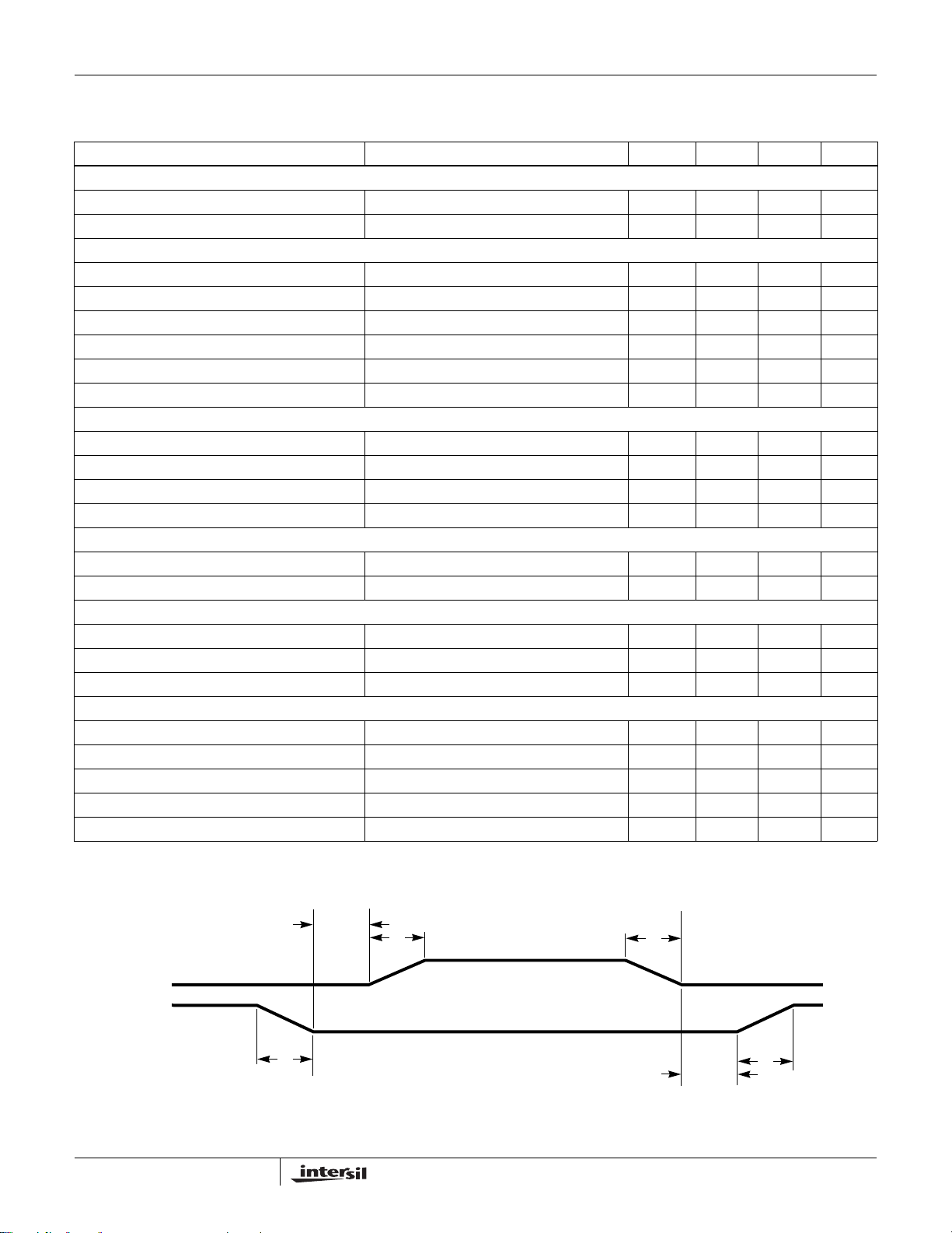
Timing Diagram
UGATE
LGATE
t
PDHUGATE
t
8
FLGATE
t
RUGATE
t
t
PDHLGATE
FUGATE
t
RLGATE
FN9278.4
October 21, 2008

ISL6323ISL6323
Functional Pin Description
VID1/SEL
This pin selects SVI or PVI mode operation based on the state
of the pin prior to enabling the ISL6323. If the pin is LO prior to
enable, the ISL6323 is in SVI mode and the dual purpo se pins
[VID0/VFIXEN, VID2/SVC, VID3/SVD] use their SVI mode
related functions. If the pin held HI prior to enable, the
ISL6323 is in PVI mode and dual purpose pins use their VIDx
related functions to de code the correct DAC co de.
VID0/VFIXEN
If VID1 is LO prior to enable [SVI Mode], the pin is functions
as the VFIXEN selection input from the AMD processor for
determining SVI mode versus VFIX mode of operation.
If VID1 is HI prior to enable [PVI Mode], the pin is used as
DAC input VID0. This pin has an internal 30µA pull-down
current applied to it at all times.
VID2/SVD
If VID1 is LO prior to enable [SVI Mode], this pin is the serial
VID data bi-directional signal to and from the master device on
AMD processor. If VID1 is HI prior to enable [PVI Mode], this
pin is used to decode the programmed DAC code for the
processor. In PVI mode, this pin has an internal 30µA pull-down
current applied to it. There is no pull-down current in SVI mode.
VID3/SVC
If VID1 is LO prior to enable [SVI Mode], this pin is the serial
VID clock input from the AMD processor . If VID1 is HI prior to
enable [PVI Mode], the ISL6323 is in PVI mode and this pin is
used to decode the programmed DAC code for the processor.
In PVI mode, this pin has an internal 30µA pull-down current
applied to it. There is no pull-down current in SVI mode.
VID4
This pin is active only when the ISL6323 is in PVI mode.
When VID1 is HI prior to enable, the ISL6323 decodes the
programmed DAC voltage required by the AMD processor.
This pin has an internal 30µA pull-down current applied to it at
all times.
VID5
This pin is active only when the ISL6323 is in PVI mode.
When VID1 is HI prior to enable, the ISL6323 decodes the
programmed DAC voltage required by the AMD processor.
This pin has an internal 30µA pull-down current applied to it at
all times.
VCC
VCC is the bias supply for the ICs small-signal circuitry.
Connect this pin to a +5V supply and decouple using a
quality 0.1µF ceramic capacitor.
PVCC1_2
The power supply pin for the multiphase internal MOSFET
drivers. Connect this pin to any voltage from +5V to +12V
depending on the desired MOSFET gate-drive level.
Decouple this pin with a quality 1.0µF ceramic capacitor.
PVCC_NB
The power supply pin for the internal MOSFET driver for the
Northbridge controller. Connect this pin to any voltage from
+5V to +12V depending on the desired MOSFET gate-drive
level. Decouple this pin with a quality 1.0µF ceramic capacitor .
GND
GND is the bias and reference ground for the IC. The GND
connection for the ISL6323 is through the thermal pad on the
bottom of the package.
EN
This pin is a threshold-sensitive (approximately 0.85V) system
enable input for the controller. Held low, this pin disab les both
CORE and NB controller operation. Pulled high, the pin
enables both controllers for operation.
When the EN pin is pulled high, the ISL6323 will be placed in
either SVI or PVI mode. The mode is determined by the
latched value of VID1 on the rising edge of the EN signal.
A third function of this pin is to provide driver bias monitor for
external drivers. A resistor divider with the center tap
connected to this pin from the drive bias supply prevents
enabling the controller before insufficient bias is provided to
external driver. The resistors should be selected such th at
when the POR-trip point of the external driver is reached, the
voltage at this pin meets the above mentioned threshold level .
FS
A resistor, placed from FS to Ground or from FS to VCC,
sets the switching frequency of both controllers. Refer to
Equation 1 for proper resistor calculation.
10.61 1.035 fs()log–[]
10
=
R
T
With the resistor tied from FS to Ground, Droop is enabled.
With the resistor tied from FS to VCC, Droop is disabled.
(EQ. 1)
VSEN and RGND
VSEN and RGND are inputs to the core voltage regulator
(VR) controller precision differential remote-sense amplifier
and should be connected to the sense pins of the remote
processor core(s), VDDFB[H,L].
FB and COMP
These pins are the internal error amplifier inverting input and
output respectively of the core VR controller. FB, VSEN and
COMP are tied together through external R-C networks to
compensate the regulator.
APA
Adaptive Phase Alignment (APA) pin for setting trip level and
adjusting time constant. A 100µA current flows into the APA
pin and by tying a resistor from this pin to COMP the trip
level for the Adaptive Phase Alignment circuitry can be set.
9
FN9278.4
October 21, 2008

ISL6323ISL6323
OFS
The OFS pin provides a means to program a DC current for
generating an offset voltage across the resistor between FB
and VSEN The offset current is generated via an external
resistor and precision internal voltage references. The polarity
of the offset is selected by connecting the resistor to GND or
VCC. For no offset, the OFS pin should be left unconnected.
ISEN1-, ISEN1+, ISEN2-, ISEN2+, ISEN3-, ISEN3+,
ISEN4-, and ISEN4+
These pins are used for differentially sensing the corresponding
channel output currents. The sensed currents are used for
channel balancing, protection, and core load line regulation.
Connect ISEN1-, ISEN2-, ISEN3-, and ISEN4- to the node
between the RC sense elements surrounding the inductor of
their respective channel. Tie the ISEN+ pins to the VCORE
side of their corresponding channel’s sense capacitor.
UGATE1 and UGATE2
Connect these pins to the corresponding upper MOSFET
gates. These pins are used to control the upper MOSFETs
and are monitored for shoot-through prevention purposes.
Maximum individual channel duty cycle is limited to 93.3%.
BOOT1 and BOOT2
These pins provide the bias voltage for the corresponding
upper MOSFET drives. Connect these pins to appropriately
chosen external bootstrap capacitors. Internal bootstrap
diodes connected to the PVCC1_2 pin provide the
necessary bootstrap charge.
PHASE1 and PHASE2
Connect these pins to the sources of the corresponding
upper MOSFETs. These pins are the return path for the
upper MOSFET drivers.
LGATE1 and LGATE2
These pins are used to control the lower MOSFET s. Connect
these pins to the corresponding lower MOSFETs’ gates.
PWM3 and PWM4
Pulse-width modulation outputs. Connect these pins to the
PWM input pins of an Intersil driver IC if 3- or 4-phase
operation is desired. Connect the ISEN- pins of the channels
not desired to +5V to disable them and configure the core
VR controller for 2-phase or 3-phase operation.
PWROK
System wide Power Good signal. If this pin is low, the two
SVI bits are decoded to determine the “metal VID”. When the
pin is high, the SVI is actively running its protocol.
RSET
Connect this pin to the VCC pin through a resistor (R
set the effective value of the internal R
resistors. The values of the R
resistor should be no less
SET
current sense
ISEN
SET
) to
than 20kΩ and no more than 80kΩ. A 0.1µF capacitor
should be placed in parallel to the R
SET
resistor.
VDDPWRGD
During normal operation this pin indicates whether both output
voltages are within specified overvoltage a nd undervoltage
limits. If either output voltage exceeds these limits or a reset
event occurs (such as an overcurrent event), the pin is pulled
low. This pin is always low pri or to the end of sof t-st art.
RGND_NB
This pin is an input to the NB VR controller precision
differential remote-sense amplifier and should be connected
to the sense pin of the North Bridge, VDDNBFBL.
DVC
The DVC pin is a buffered version of the reference to the error
amplifier. A series resistor and capaci tor between the DVC pin
and FB pin smooth the voltage transition d uring VID-on-the-fly
operations.
FB_NB and COMP_NB
These pins are the internal error amplifier inverting input and
output respectively of the NB VR controller. FB_NB,
VDIFF_NB, and COMP_NB are tied together through
external R-C networks to compensate the re gu l at o r.
ISEN_NB-, ISEN_NB+
These pins are used for differentially sensing the North
Bridge output current. The sensed current is used for
protection and load line regulation if droop is enabled.
Connect ISEN_NB- to the node between the RC sense
element surrounding the inductor. Tie the ISEN_NB+ pin to
the VNB side of the sense capacitor.
UGATE_NB
Connect this pin to the corresponding upper MOSFET gate.
This pin provides the PWM-controlled gate drive for the
upper MOSFET and is monitored for shoot-through
prevention purposes.
BOOT_NB
This pin provides the bias voltage for the corresponding
upper MOSFET drive. Connect this pin to appropriately
chosen external bootstrap capacitor. The internal bootstrap
diode connected to the PVCC_NB pin provides the
necessary bootstrap charge.
PHASE_NB
Connect this pin to the source of the corresponding upper
MOSFET. This pin is the return path for the upper MOSFET
drive. This pin is used to monitor the voltage drop across the
upper MOSFET for overcurrent protection.
LGATE_NB
Connect this pin to the corresponding MOSFET’s gate. This
pin provides the PWM-controlled gate drive for the lower
MOSFET. This pin is also monitored by the adaptive
10
FN9278.4
October 21, 2008
ISL6323
shoot-through protection circuitry to determine when the
lower MOSFET has turned off.
Operation
The ISL6323 utilizes a multiphase architecture to provide a
low cost, space saving power conversion solution for the
processor core voltage. The controller also implements a
simple single phase architecture to provide the Northbridge
voltage on the same chip.
Multiphase Power Conversion
Microprocessor load current profiles have changed to the
point that the advantages of multiphase power conversion
are impossible to ignore. The technical challenges
associated with producing a single-phase converter that is
both cost-effective and thermally viable have forced a
change to the cost-saving approach of multiphase. The
ISL6323 controller helps simplify implementation by
integrating vital functions and requiring minimal external
components. The “Controller Block Diagram” on page 3
provides a top level view of the multiphase power conversion
using the ISL6323 controller.
Interleaving
The switching of each channel in a multiphase converter is
timed to be symmetrically out-of-phase with each of the other
channels. In a 3-phase converter, each channel switches 1/3
cycle after the previous channel and 1/3 cycle before the
following channel. As a result, the 3-phase converter has a
combined ripple frequency 3x greater than the ripple frequency
of any one phase. In addition, the peak-to-peak amplitude of
the combined inductor currents is reduced in proportion to the
number of phases (Equations 2 and 3). Increased ripple
frequency and lower ripple amplitude mean that the designer
can use less per-channel inductance and lower total output
capacitance for any performance specification.
The output capacitors conduct the ripple component of the
inductor current. In the case of multiphase converters, the
capacitor current is the sum of the ripple currents from each
of the individual channels. Compare Equation 2 to the
expression for the peak-to-peak current after the summation
of N symmetrically phase-shifted inductor currents in
Equation 3. Peak-to-peak ripple current decreases by an
amount proportional to the number of channels. Output
voltage ripple is a function of capacitance, capacitor
equivalent series resistance (ESR), and inductor ripple
current. Reducing the inductor ripple current allows the
designer to use fewer or less costly output capacitors.
I
CP-P()
------------------------------------------------------------=
LfSV
OUT
IN
(EQ. 3)
VINNV
–()V
OUT
Another benefit of interleaving is to reduce input ripple
current. Input capacitance is determined in part by the
maximum input ripple current. Multiphase topologies can
improve overall system cost and size by lowering input ripple
current and allowing the designer to reduce the cost of input
capacitance. The example in Figure 2 illustrates input
currents from a 3-phase converter combining to reduce the
total input ripple current.
The converter depicted in Figure 2 delivers 1.5V to a 36A load
from a 12V input. The RMS input capacitor current is 5.9A.
Compare this to a single-phase conve rter also step ping down
12V to 1.5V at 36A. The single-phase converter has
11.9A
input capacitor current. The single-phase converter
RMS
must use an input capacitor bank with twice the RMS current
capacity as the equivalent 3-phase converter.
Figures 25, 26 and 27 in the section entitled “Input Capacitor
Selection” on page 31 can be used to determine the input
capacitor RMS current based on load current, duty cycle,
and the number of channels. They are provided as aids in
determining the optimal input capacitor solution.
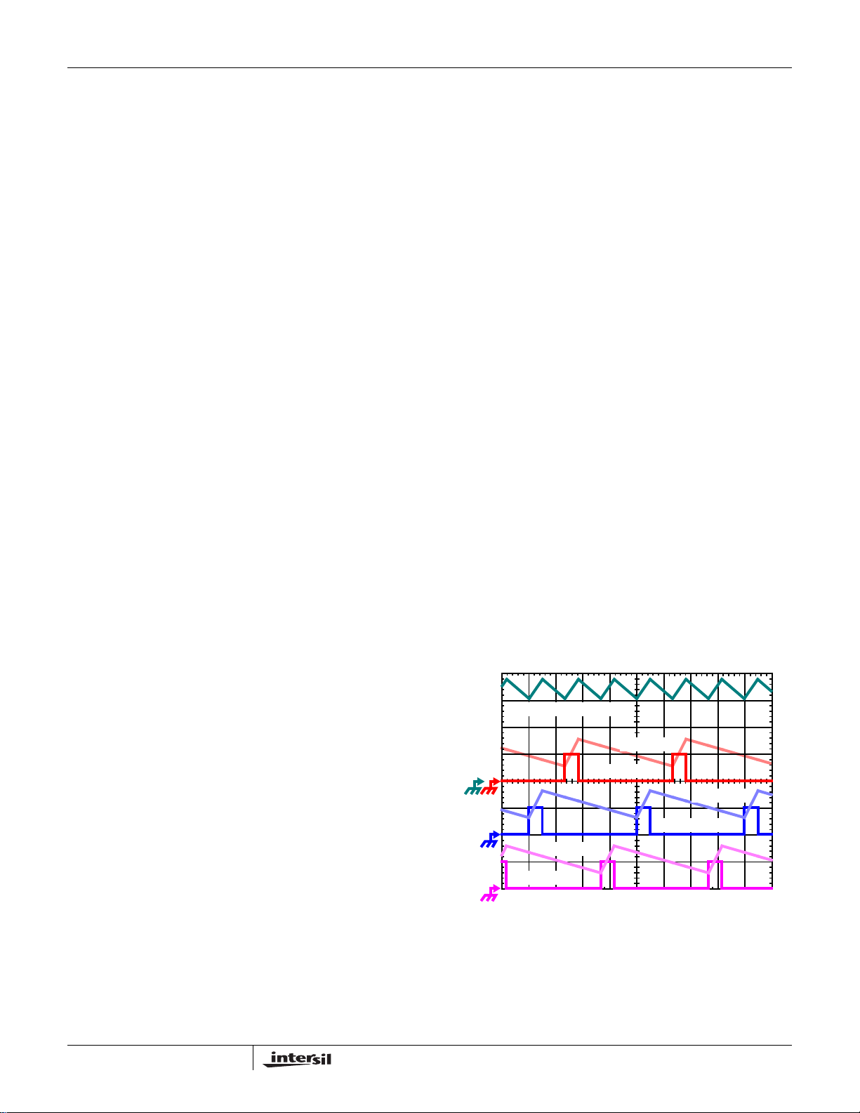
Figure 1 illustrates the multiplicative effect on output ripple
frequency. The 3-channel currents (IL1, IL2, and IL3)
combine to form the AC ripple current and the DC load
current. The ripple component has 3x the ripple frequency of
each individual channel current. Each PWM pulse is
terminated 1/3 of a cycle after the PWM pulse of the previous
phase. The peak-to-peak current for each phase is about 7A,
and the DC components of the inductor current s combin e to
feed the load.
T o understand the reduction of ripple current amplitude in the
multiphase circuit, examine the equation representing an
individual channel peak-to-peak inductor current.
I
------------------------------------------------------=
PP–
LfSV
In Equation 2, V
and V
IN
IN
OUT
are the input and output
OUT
(EQ. 2)
VINV
–()V
OUT
voltages respectively, L is the single-channel inductor value,
and f
is the switching frequency.
S
11
IL1 + IL2 + IL3, 7A/DIV
IL3, 7A/DIV
PWM3, 5V/DIV
IL2, 7A/DIV
PWM2, 5V/DIV
IL1, 7A/DIV
PWM1, 5V/DIV
1µs/DIV
FIGURE 1. PWM AND INDUCTOR-CURRENT WA VEFORMS
FOR 3-PHASE CONVERTER
FN9278.4
October 21, 2008
 Loading...