

Page 1
®
ISL6298EVAL2 Evaluation Board
Application Manual
Application Note AN1172.0February 9, 2005
Description
The ISL6298EVAL2 provides a complete platform for the
evaluation of the ISL6298-2CR4. The on board 9-bit DIP
switch facilitates programming charging current, setting EN
input, battery thermal status, and so on. The four jumpers
can set up input source selection, USB mode selection, and
can be used to make other necessary connections.
Assembled in the center, the components constitute a
complete charger solution, demonstrating the space saving
advantage of the ISL6298 in limited space applications.
LEDs connected to FAULT and STATUS pins will indicate
the normal charging status or fault condition.
On board jumpers and a DIP switch accommodate different
operation conditions for the charger.
Ordering Information
PART # DESCRIPTION
ISL6298EVAL2 Evaluation Board for the ISL6298-2CR4
Features:
• 9-bit DIP switch for conveniently setting up charging
current, battery thermal status, EN input, and so on
• Different jumpers for input source selection, USB mode
selection, and the convenience of current measurement
• Exposed soldering pads connected to STATUS, FAULT,
TIME, EN, V2P8, IMIN and TEMP functional pins to
accommodate experimental testing that need extra
connections to those pins
• Board size 3.5 x 2.5 square inches for the convenience of
evaluation
• Eight thermal vias in the thermal pad simulating the
customers’ thermal enhanced environment
Pinout
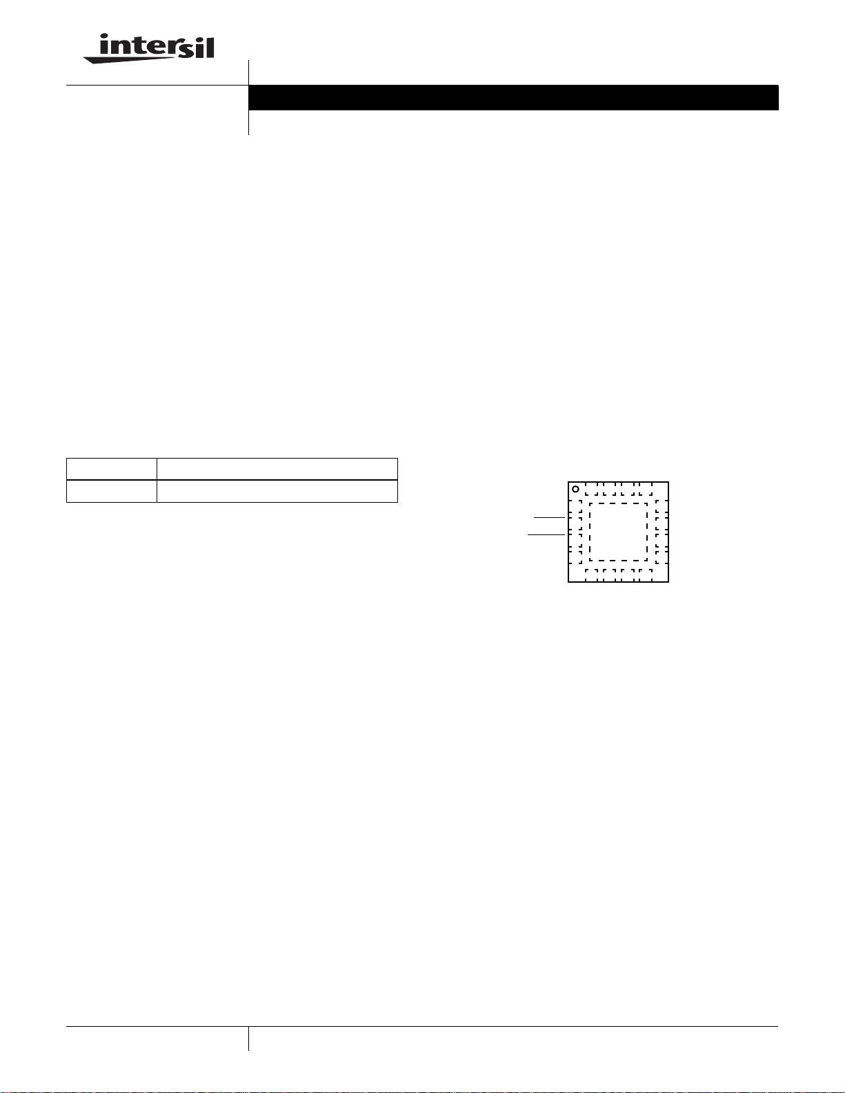
ISL6298 (16 LEAD QFN)
TOP VIEW
VIN
VIN
VBAT
VBAT
12
11
10
9
6578
EN
V2P8
TOEN
VBAT
TEMP
IMIN
IREF
VIN
FAULT
STATUS
TIME
16 14 13
15
1
2
3
4
GND
1
CAUTION: These devices are sensitive to electrostatic discharge; follow proper IC Handling Procedures.
1-888-INTERSIL or 1-888-352-6832
| Intersil (and design) is a registered trademark of Intersil Americas Inc.
All other trademarks mentioned are the property of their respective owners.
Copyright Intersil Americas Inc. 2005. All Rights Reserved
Page 2
Application Note 1172
What is inside
The Evaluation Kit contains:
• ISL6298EVAL2 board
• The ISL6298 Data Sheet
• This ISL6298EVAL2 Application Note
What is needed
The following instruments will be needed to perform testing:
• Power supplies:
1 PS1: DC 20V/5A,
2 PS2: DC (sinks current) 20V/5A, such as
Agilent 6654A)
• Electronic load: 20V/5A
• Multimeters
• Function generator
• Oscilloscope
• Cables and wires
Quick Setup Guide
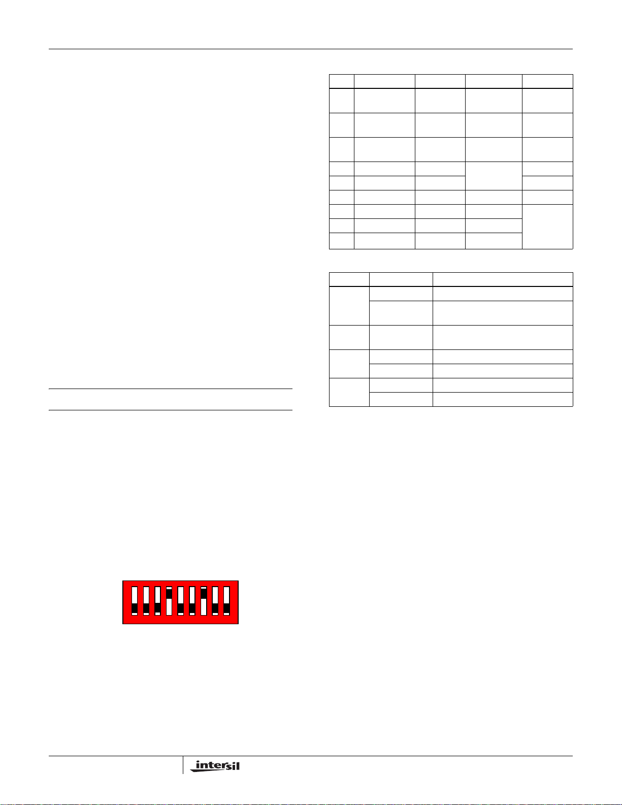
Step 1: Switch on bit 4 and bit 7 of the Dip-switch. Leave
all other bits off, (See Figure 1.)
DO NOT APPLY POWER UNTIL STEP 6
.
BIT DESCRIPTION ON OFF REMARK
JUMPER POSITION FUNCTION
TABLE 1. DIP SWITCH PIN DESCRIPTIONS
Adjustable
1
TIMEOUT
TIMEOUT
2
disable/enable
Charger
3
enable/disable
4 IREF setting 1 Add 125mA I
5 IREF setting 2 Add 250mA
6 IMIN setting 25mA 12.5mA
7 TEMP normal Normal All off
8 TEMP high Too hot
TEMP low Too cold
9
USB TO VIN USB input selected
JP1
WALL CUBE TO
VIN
Shunt Installed Connect VBAT pin to battery
JP2
shunt installed Battery attached to Thermistor at J2
JP3
not installed Default
IREF and V2P8 Setting USB 255mA mode
JP4
IREF and GND Setting USB 100mA mode
5 hours
50 mins
TIMEOUT
disabled
Charger
disabled
TABLE 2. JUMPER SETTINGS
Wall adapter input selected
Current meter can replace shunt
3 hours
30 mins
TIMEOUT
enabled
Charger
enabled
=125mA
CHG
When both off
simulates
battery
removal
Step 2: Connect 5V on VIN.
Step 3: Connect 3.7V on VBAT.
Step 4: Connect 500mA electronic load on VBAT.
Step 5: Verify that no shunts across all jumpers.
Step 6: Turn on Power Supplies and electronic load.
Step 7: Green LED should be on, indicating normal
charging operation.
Step 8: If current meter is in series with VIN, it shall read
250mA as the charging current.
O N
O F F
1
23456789
FIGURE 1. INITIAL DIP SWITCH SETTINGS
DIP Switch Settings
A 9-bit DIP switch is provided to set up voltage, current
reference, end-of-charge (EOC) current, and so on. The
functionality of the bits are described in Table 1.
Initial Board Jumper Positioning (Refer to Figure 3)
JP1 - Selects the VIN pin to be connected to either a wall
adapter, or to a USB connector. If the J1 connector is being
used, a shunt must be installed across ‘WALL CUBE TO
VIN’, or if the J3 (USB) connector is being used, a shunt
must be installed across ‘USB TO VIN’. J1, J3 and JP1 can
be ignored if the power supply is connected directly to the
VIN test point, which is directly connected to the VIN pin of
the IC. A current meter, to measure the input current, can
replace the shunt mentioned above.
JP2 - Can connect the VBAT pin to the battery. If the J2
connector is being used, a shunt must be installed across
JP2. In this case, a current meter can also replace the shunt
to measure the VBAT current.
JP3 - Can connect the TEMP pin to the battery. Usually no
shunt is needed for JP3, as the Eval board can simulate
various battery thermal conditions. Only when a battery with
an attached thermistor is applied on J2 does it become
necessary to install a shunt across JP3, simultaneously
turning off bits 7, 8, and 9 on the DIP switch.
JP4 - Selects USB modes; a shunt across IREF and V2P8
will set USB 255mA mode, a shunt across IREF and GND
will set USB 100mA mode. When the charge current is
programmed by the resistors connected to IREF pin, no
shunt should be installed on JP4.
2
AN1172.0
February 9, 2005
Page 3
Application Note 1172
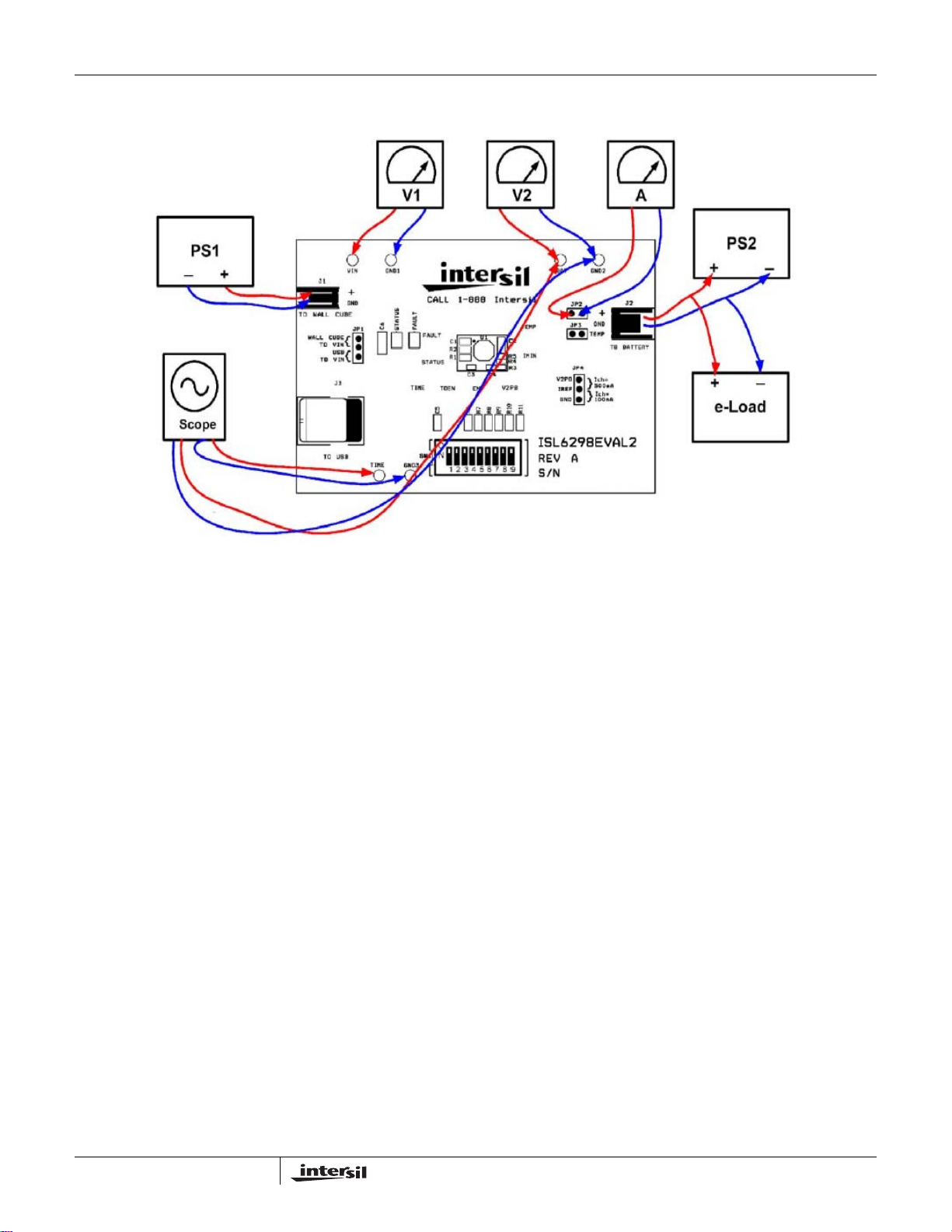
FIGURE 2. CONNECTION OF INSTRUMENTS
3
AN1172.0
February 9, 2005
Page 4
Board Layout Information
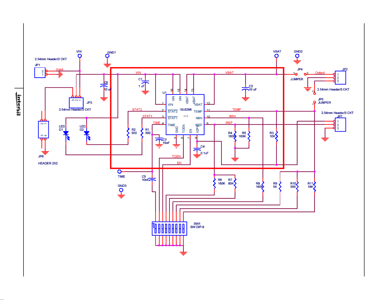
Schematics of PCB board
4
Application Note 1172
February 9, 2005
AN1172.0
FIGURE 3. BOARD LAYOUT INFORMATION SCHEMATIC
Page 5

Application Note 1172
TABLE 3. ISL6298EVAL2 BILL OF MATERIALS
ITEM QUANTITY REFERENCE PART DESCRIPTION PCB FOOTPRINT PART NUMBER VENDOR
1 1 C1 1µF, 6.3V, X5R ceramic cap 0603 0603X105K6R3 Walsin
2 1 C2 10µF/6.3V, Tantalum Cap 2.05 x 1.3 x 1.2 TAJR106M006 AVX
3 1 C3 15nF/16V, X7R ceramic cap 0402 C1005X7R1C153K TDK
4 1 C4 0.1µF/16V, Y5V ceramic cap 0402 C1005Y5V1C104ZT TDK
5 1 C5 10nF/16V, X7R Ceramic cap 0805 C1005X7R1C103K TDK
6 1 C6 10µF/16V, Tantalum Cap 3.2 x1.6 x 1.6 TAJA106M016 AVX
7 1 D1 Green LED 0805 67-1553-1-ND DigiKey
8 1 D2 Red LED 0805 67-1552-1-ND DigiKey
9 2 R1, R2 1K, 5% 0603 Various
10 1 R3 10K, 1% 0603 Various
11 2 R4, R5 160K, 1% 0603 Various
12 1 R6 160K, 1% 0805 Various
13 1 R7 80K, 1% 0805 Various
14 1 R8 160K, 1% 0805 Various
15 1 R9 5K, 1% 0805 Various
16 1 R10 500, 1% 0805 Various
17 1 R11 18K, 1% 0805 Various
18 1 J1 2.54mm Male Header, 2 ckt (R/A) A23879-ND DigiKey
19 1 J2 2.54mm Male Header, 3 ckt (R/A) A23880-ND DigiKey
20 2 JP1, JP4 2.54mm Male Header, 3ckt WM6403-ND DigiKey
21 2 JP2, JP3 2.54mm Male Header, 2 ckt WM6402-ND DigiKey
22 1 J3 USB receptacle, B type 787780-1-ND DigiKey
23 1 SW1 DIP Switch, 9 Pos, SMT CKN1323-ND DigiKey
24 1 U1 Single-Cell Li-ion Battery Charger 16-pin, 4 x 4 QFN ISL6298 Intersil
25 6 VIN, VBAT,
TIME, GND1,
GND2, GND3
Test Point 5002K-ND DigiKey
5
AN1172.0
February 9, 2005
Page 6

PCB Layout
Application Note 1172
SILK SCREEN LAYER INTERNAL (LAYER 2, GND)
BOTTOM (LAYER 4, GND) TOP (LAYER 1, SIGNAL)
INTERNAL (LAYER 3, FLOATING)
Intersil Corporation reserves the right to make changes in circuit design, software and/or specifications at any time without notice. Accordingly, the reader is cautioned to
verify that the Application Note or Technical Brief is current before proceeding.
For information regarding Intersil Corporation and its products, see www.intersil.com
6
AN1172.0
February 9, 2005
Page 7

Authorized Distribution Brand:
Website:
Welcome to visit www.ameya360.com
Contact Us:
Address:
401 Building No.5, JiuGe Business Center, Lane 2301, Yishan Rd
Minhang District, Shanghai , China
Sales:
Direct +86 (21) 6401-6692
Email [email protected]
QQ 800077892
Skype ameyasales1 ameyasales2
Customer Service:
Email [email protected]
Partnership:
Tel +86 (21) 64016692-8333
Email [email protected]
 Loading...