

Page 1
¬
ISL6292
Data Sheet December 17, 2007
Li-ion/Li Polymer Battery Charger
The ISL6292 is an integrated single-cell Li-ion or Li-polymer
battery charger capable of operating with an input voltage as
low as 2.4V. This charger is designed to work with various
types of AC adapters or a USB port.
The ISL6292 operates as a linear charger when the AC
adapter is a voltage source. The battery is charged in a
CC/CV (constant current/const ant voltage) profile. The
charge current is programmable with an external resistor up
to 2A. The ISL6292 can also work with a current-limited
adapter to minimize the thermal dissipation, in which case,
the ISL6292 combines the benefits of both a linear charger
and a pulse charger.
The ISL6292 features charge current thermal foldback to
guarantee safe operation when the printed circuit board is
space limited for thermal dissipation. Additional features
include preconditioning of an over-discharged battery, an
NTC thermistor interface for charging the battery in a safe
temperature range, automatic recharge, and thermally
enhanced QFN or DFN packages.
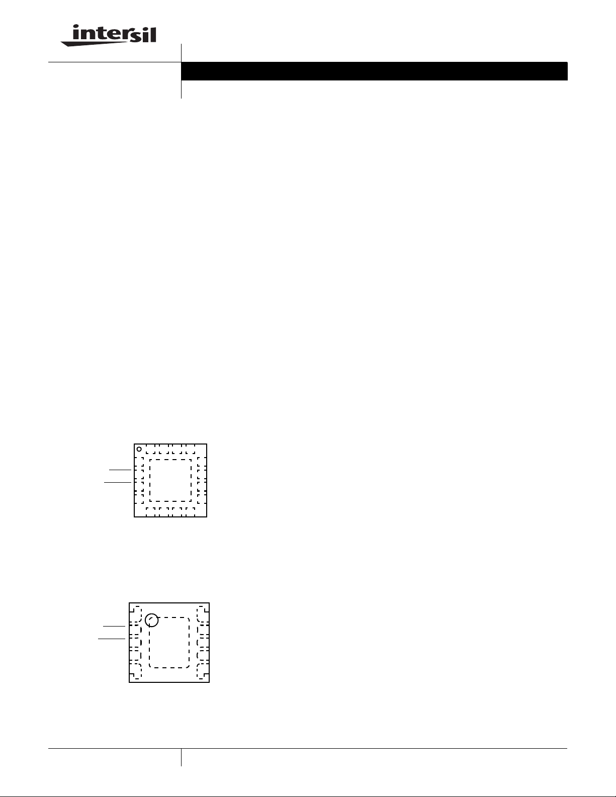
Pinouts
ISL6292
(16 LD QFN)
TOP VIEW
VIN
VIN
VBAT
VBAT
12
11
10
9
6578
EN
V2P8
TOEN
VBAT
TEMP
IMIN
IREF
VIN
FAULT
STATUS
TIME
16 14 13
15
1
2
3
4
GND
FN9105.9
Features
• Complete Charger for Single-Cell Li-ion Batteries
• Very Low Thermal Dissipation
• Integrated Pass Element and Current Sensor
• No External Blocking Diode Required
• 1% Voltage Accuracy
• Programmable Current Limit up to 2A
• Programmable End-of-Charge Current
• Charge Current Thermal Foldback
• NTC Thermistor Interface for Battery Temperature Monitor
• Accepts Multiple T ypes of Adapters or USB BUS Power
• Guaranteed to Operate at 2.65V After Start-Up
• Ambient Temperature Range: -20°C to +70°C
• Thermally-Enhanced QFN Packages
• Handheld Devices, including Medical Handhelds
• PDAs, Cell Phones and Smart Phones
• Portable Instruments, MP3 Players
• Self-Charging Battery Packs
• Stand-Alone Chargers
• USB Bus-Powered Chargers
• Pb-Free Available (RoHS Compliant)
Related Literature
• Technical Brief TB363 “Guidelines for Handling and
Processing Moisture Sensitive Surface Mount Devices
(SMDs)”
• Technical Brief TB379 “Thermal Characterization of
Packaged Semiconductor Devices”
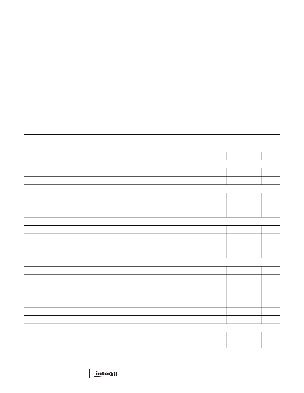
VIN
FAULT
STATUS
TIME
GND
ISL6292
(10 LD DFN)
TOP VIEW
1
2
3
4
5
• Technical Brief TB389 “PCB Land Pattern Design and
Surface Mount Guidelines for QFN Packages”
10
VBAT
9
TEMP
8
IREF
7
V2P8
6
EN
1
CAUTION: These devices are sensitive to electrostatic discharge; follow proper IC Handling Procedures.
1-888-INTERSIL or 1-888-468-3774
| Intersil (and design) is a registered trademark of Intersil Americas Inc.
All other trademarks mentioned are the property of their respective owners.
Copyright Intersil Americas Inc. 2003-2007. All Rights Reserved
Page 2

2
Page 3
ISL6292
Absolute Maximum Ratings Thermal Information
Supply Voltage (VIN) . . . . . . . . . . . . . . . . . . . . . . . . . . . .-0.3V to 7V
Output Pin Voltage (BAT). . . . . . . . . . . . . . . . . . . . . . . -0.3V to 5.5V
Signal Input Voltage (TOEN, TIME, IREF, IMIN) . . . . . -0.3V to 3.2V
Output Pin Voltage (STATUS, FAULT). . . . . . . . . . . . . . .-0.3V to 7V
Charge Current (For 4x4 or 5x5 QFN Packages) . . . . . . . . . . . 2.1A
Charge Current (For 3x3 DFN Package) . . . . . . . . . . . . . . . . . 1.6A
Recommended Operating Conditions
Ambient Temperature Range. . . . . . . . . . . . . . . . . . .-20°C to +70°C
Supply Voltage, VIN. . . . . . . . . . . . . . . . . . . . . . . . . . . 4.3V to 6.5V
CAUTION: Do not operate at or near the maximum ratings listed for extended periods of time. Exposure to such conditions may adversely impact product reliability and
result in failures not covered by warranty.
NOTES:
is measured in free air with the component mounted on a high effective thermal conductivity test board with “direct attach” features. See
1. θ
JA
Tech Brief TB379.
, “case temperature” location is at the center of the exposed metal pad on the package underside. See Tech Brief TB379.
2. θ
JC
Thermal Resistance (Junction to Ambient) θ
(°C/W) θJC (°C/W)
JA
5x5 QFN Package (Notes 1, 2) . . . . . . 34 4
4x4 QFN Package (Notes 1, 2) . . . . . . 41 4
3x3 DFN Package (Notes 1, 2) . . . . . . 46 4
Maximum Junction Temperature (Plastic Package) . . . . . . .+150°C
Maximum Storage Temperature Range. . . . . . . . . .-65°C to +150°C
Pb-free reflow profile . . . . . . . . . . . . . . . . . . . . . . . . . .see link below
http://www.intersil.com/pbfree/Pb-FreeReflow.asp
Electrical Specifications Typical values are tested at V
= 5V and +25°C Ambient Temperature, maximum and minimum values are
IN
guaranteed over 0°C to +70°C Ambient Temperature with a supply voltage in the range of 4.3V to 6.5V, unless
otherwise noted.
PARAMETER SYMBOL TEST CONDITIONS MIN TYP MAX UNITS
POWER-ON RESET
Rising VIN Threshold 3.0 3.4 4.0 V
Falling VIN Threshold 2.11 2.4 2.65 V
STANDBY CURRENT
VBAT Pin Sink Current I
STANDBY
VIN Pin Supply Current I
VIN Pin Supply Current I
VIN
VIN
VIN floating or EN = LOW - - 3.0 µA
VBAT floating and EN pulled low - 30 - µA
VBAT floating and EN floating - 1 - mA
VOLTAGE REGULATION
Output Voltage V
Output Voltage V
CH
CH
ISL6292-1 4.059 4.10 4.141 V
ISL6292-2 4.158 4.20 4.242 V
Dropout Voltage VBAT = 3.7V, 0.5A, 4x4 or 5x5 package - 140 - mV
Dropout Voltage VBAT = 3.7V, 0.5A, 3x3 package - 175 - mV
CHARGE CURRENT
Constant Charge Current I
Trickle Charge Current I
Constant Charge Current I
Trickle Charge Current I
Constant Charge Current I
Trickle Charge Current I
CHARGERIREF
TRICKLE
CHARGE
TRICKLE
CHARGE
TRICKLE
End-of-Charge Threshold R
= 80kΩ, V
R
= 80kΩ, V
IREF
IREF Pin Voltage > 1.2V, V
IREF Pin Voltage > 1.2V, V
IREF Pin Voltage < 0.4V, V
IREF Pin Voltage < 0.4V, V
= 80kΩ 85 110 135 mA
IMIN
= 3.7V 0.9 1.0 1.1 A
BAT
= 2.0V - 110 - mA
BAT
= 3.7V 400 450 520 mA
BAT
= 2.0V - 45 - mA
BAT
= 3.7V - - 100 mA
BAT
= 2.0V - 10 - mA
BAT
RECHARGE THRESHOLD
Recharge Voltage Threshold V
Recharge Voltage Threshold V
RECHRG
RECHRG
ISL6292-2 - 4.0 - V
ISL6292-1 - 3.90 - V
3
FN9105.9
December 17, 2007
Page 4
ISL6292
Electrical Specifications Typical values are tested at V
guaranteed over 0°C to +70°C Ambient Temperature with a supply voltage in the range of 4.3V to 6.5V, unless
= 5V and +25°C Ambient Temperature, maximum and minimum values are
IN
otherwise noted. (Continued)
PARAMETER SYMBOL TEST CONDITIONS MIN TYP MAX UNITS
TRICKLE CHARGE THRESHOLD
Trickle Charge Threshold Voltage V
MIN
2.7 2.8 3.0 V
TEMPERATURE MONITORING
Low Battery Temperature Threshold V
High Battery Temperature Threshold V
Battery Removal Threshold V
Charge Current Foldback Threshold T
Current Foldback Gain G
TMIN
TMAX
RMV
FOLD
FOLD
V2P8 = 3.0V 1.45 1.51 1.57 V
V2P8 = 3.0V 0.36 0.38 0.40 V
V2P8 = 3.0V - 2.25 - V
85 100 115 °C
-100-mA/°C
OSCILLATOR
C
Oscillation Period t
OSC
= 15nF 2.4 3.0 3.6 ms
TIME
LOGIC INPUT AND OUTPUT
TOEN Input High 2.0 - - V
TOEN and EN Input Low --0.8V
IREF and IMIN Input High 1.2 - - V
IREF and IMIN Input Low --0.4V
STATUS/FAULT Sink Current Pin Voltage = 0.8V 5 - - mA
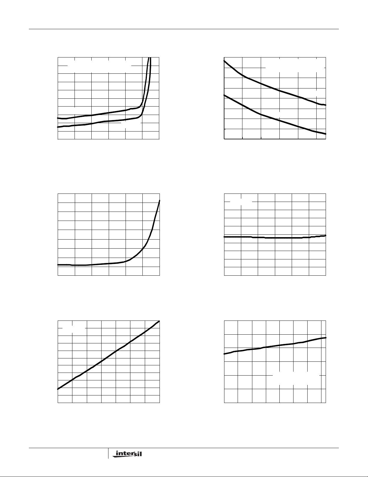
Typical Operating Performance The test conditions for the Typical Operating Performance are: V
R
IREF
4.2015
4.2010
R
4.2005
4.2000
(V)
4.1995
BAT
V
4.1990
4.1985
4.1980
4.1975
0 0.3 0.6 0.9 1.2 1.5
CHARGE CURRENT (A)
IREF
= 40kΩ
FIGURE 1. CHARGER OUTPUT VOLTAGE vs CHARGE
CURRENT
= R
IMIN
= 80kΩ, V
= 3.7V, Unless Otherwise Noted.
BAT
4.210
4.208
4.206
4.204
4.202
(V)
4.200
BAT
4.198
V
4.196
4.194
4.192
4.190
0 20 40 60 80 100 120
CHARGE CURRENT = 50mA
TEMPERATURE (°C)
FIGURE 2. CHARGER OUTPUT VOLTAGE vs TEMPERATURE
= 5V, TA = +25°C,
IN
4
FN9105.9
December 17, 2007
Page 5
ISL6292
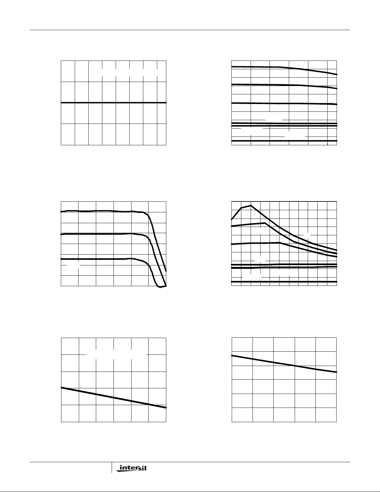
Typical Operating Performance The test conditions for the Typical Operating Performance are: V
R
IREF
4.30
CHARGE CURRENT = 50mA
4.25
(V)
4.20
BAT
V
4.15
4.10
4.2 4.5 4.8 5.1 5.4 5.7 6.0 6.3
VIN (V)
FIGURE 3. CHARGER OUTPUT VOLT AGE vs INPUT
= R
IMIN
= 80kΩ, V
= 3.7V, Unless Otherwise Noted. (Continued)
BAT
2.0
1.8
1.6
1.4
1.2
1.0
0.8
0.6
CHARGE CURRENT (A)
0.4
0.2
USB500
0
3.0 3.2 3.4 3.6 3.8 4.0
0.5A
V
FIGURE 4. CHARGE CURRENT vs OUTPUT VOLTAGE
1A
BAT
IN
1.5A
USB100
(V)
= 5V, TA = +25°C,
2A
VOLTAGE CHARGE CURRENT = 50mA
1.6
1.4
1.2
1.0
0.8
0.6
0.5A
0.4
CHARGE CURRENT (A)
0.2
0.0
0 20 40 60 80 100 120
1.5A
1.0A
TEMPERATURE (°C)
2.0
1.8
1.6
1.4
1.2
1.0
0.8
0.6
CHARGE CURRENT (A)
0.4
0.2
0
4.3 4.5 4.7 4.9 5.1 5.3 5.5 5.7 5.9 6.1 6.3 6.5
USB100
1.5A
0.5A
1A
USB500
VIN (V)
2A
FIGURE 5. CHARGE CURRENT vs AMBIENT TEMPERATURE FIGURE 6. CHARGE CURRENT vs INPUT VOLTAGE
2.930
2.928
)
V
(
E
2.926
G
A
T
L
O
V
2.924
8
P
2
V
2.922
2.920
3.5 4.0 4.5 5.0 5.5 6.0 6.5
V2P8 PIN LOADED WITH 2mA
(V)
V
IN
3.00
2.95
)
V
(
2.90
E
G
TA
2.85
L
O
V
8
2.80
P
2
V
2.75
2.70
0246810
V2P8 LOAD CURRENT (mA)
FIGURE 7. V2P8 OUTPUT vs INPUT VOLTAGE FIGURE 8. V2P8 OUTPUT vs ITS LOAD CURRENT
5
December 17, 2007
FN9105.9
Page 6
ISL6292
Typical Operating Performance The test conditions for the Typical Operating Performance are: V
R
= R
IREF
700
650
600
550
500
(mΩ)
450
400
DS(ON)
r
350
300
250
200
FIGURE 9. r
1.8
1.6
1.4
1.2
1.0
0.8
0.6
LEAKAGE CURRENT (µA)
0.4
BAT
V
0.2
0.0
THERMAL FOLDBACK STARTS
NEAR +100°C
3x3 DFN
4x4 QFN
0 20 40 60 80 100 120
TEMPERATURE (°C)
vs TEMPERATURE AT 3.7V OUTPUT FIGURE 10. r
DS(ON)
0 20 40 60 80 100 120
TEMPERATURE (°C)
FIGURE 11. REVERSE CURRENT vs TEMPERATURE FIGURE 12.
IMIN
= 80kΩ, V
= 3.7V, Unless Otherwise Noted. (Continued)
BAT
420
400
380
360
(mΩ)
340
320
DS(ON)
r
300
280
260
3.0 3.2 3.4 3.6 3.8 4.0
vs OUTPUT VOLTAGE USING CURRENT
DS(ON)
LIMITED ADAPTERS
50
EN = GND
45
40
35
30
25
20
15
QUIESCENT CURRENT (µA)
10
IN
V
5
0
0 20 40 60 80 100 120
500mA CHARGE CURRENT,
R
IREF
4x4 QFN
V
BAT
TEMPERATURE (°C)
INPUT QUIESCENT CURRENT vs TEMPERATURE
= 5V, TA = +25°C,
IN
= 40kΩ
(V)
3x3 DFN
32
30
EN = GND
28
26
24
22
20
18
16
14
QUIESCENT CURRENT (µA)
IN
12
V
10
3.0 3.5 4.0 4.5 5.0 5.5 6.0 6.5
VIN (V)
FIGURE 13. INPUT QUIESCENT CURRENT vs INPUT
VOLTAGE WHEN SHUTDOWN
6
1.10
1.05
1.00
0.95
0.90
QUIESCENT CURRENT (mA)
0.85
IN
V
0.80
4.3 4.6 4.9 5.2 5.5 5.8 6.1 6.4
BOTH VBAT AND EN
PINS FLOATING
VIN (V)
FIGURE 14. INPUT QUIESCENT CURRENT vs INPUT
VOLTAGE WHEN NOT SHUTDOWN
December 17, 2007
FN9105.9
Page 7
ISL6292
Typical Operating Performance The test conditions for the Typical Operating Performance are: V
R
= R
IREF
28
24
20
16
12
8
4
STATUS PIN CURRENT (mA)
0
0.0 0.5 1.0 1.5 2.0 2.5 3.0 3.5 4.0 4.5 5.0
FIGURE 15. STATUS/FAULT PIN VOLTAGE vs CURRENT WHEN THE OPEN-DRAIN MOSFET TURNS ON
Pin Descriptions
VIN (Pin 1, 15, 16 for 4x4, 5x5; Pin 1 for 3x3)
VIN is the input power source. Connect to a wall adapter.
FAULT (Pin 2)
FAULT is an open-drain output indicating fault status. This
pin is pulled to LOW under any fault conditions.
STATUS (Pin 3)
ST ATUS is an open-drain output indicating charging and
inhibit states. The STATUS
charger is charging a battery.
Time (Pin 4)
The TIME pin determines the oscillation period by
connecting a timing capacitor between this pin and GND.
The oscillator also provides a time reference for the charger.
GND (Pin 5)
GND is the connection to system ground.
TOEN (Pin 6 for 4x4, 5x5; N/A for 3x3)
TOEN is the TIMEOUT enable input pin. Pulling this pin to
LOW disables the TIMEOUT charge-time limit for the fast
charge modes. Leaving this pin HIGH or floating enables the
TIMEOUT limit.
pin is pulled LOW when the
= 80kΩ, V
IMIN
STATUS PIN VOLTAGE (V)
= 3.7V, Unless Otherwise Noted. (Continued)
BAT
EN (Pin 7 for 4x4, 5x5; Pin 6 for 3x3)
EN is the enable logic input. Connect the EN pin to LOW to
disable the charger or leave it floating to enable the charger.
V2P8 (Pin 8 for 4x4, 5x5; Pin 7 for 3x3)
This is a 2.8V reference voltage output. This pin outputs a
2.8V voltage source when the input voltage is above POR
threshold and outputs zero otherwise. The V2P8 pin can be
used as an indication for adapter presence.
IREF (Pin 9 for 4x4, 5x5; Pin 8 for 3x3)
This is the programming input for the constant charging
current.
IMIN (Pin 10 for 4x4, 5x5; N/A for 3x3)
IMIN is the programmable input for the end-of-charge
current.
TEMP (Pin 11 for 4x4, 5x5; Pin 9 for 3x3)
TEMP is the input for an external NTC thermistor. The TEMP
pin is also used for battery removal detection.
VBAT (Pin 12, 13, 14 for 4x4, 5x5; Pin 10 for 3x3)
VBAT is the connection to the battery. Typically a 10µF
Tantalum capacitor is needed for stability when there is no
battery attached. When a battery is attached, only a 0.1µF
ceramic capacitor is required.
= 5V, TA = +25°C,
IN
7
FN9105.9
December 17, 2007
Page 8

ISL6292
Typical Applications
Typical Application Circuit For 4x4 or 5x5 QFN Package Options
5V W all
Adapter
VIN
Fμ1
1kΩ
C
1
R
D
1kΩ
R
1
1
2
D
2
Fμ1
C
3
TOEN
FAULT
STATUS
EN
V2P8
TIME
C
TIME
VBAT
ISL6292
TEMP
GND
IREF
IMIN
1 F
μ
V2P8
C
2
R
R
U
T
R
IM IN
Ωk80
R
IREF
Ωk80
Battery
Pack
T
nF15
8
FN9105.9
December 17, 2007
Page 9
ISL6292
Typical Applications (Continued)
Typical Application Circuit For 3x3 DFN Package Option
5V W all
Adapter
C
1
R
R
IREF
IREF
IMIN
TEMP
TOEN
TIME
GND
VIN
IMIN
μ
1
F
C
1
Temperature
References
I
SEN
Interface
1kΩ
R
1
D
1
Monitoring
I
R
Current
I
MIN
V2P8
NTC
OSC
1kΩ
R
D
I
T
Trickle/Fast
+
-
Under Temp
Over Temp
Batt Removal
ISL6292
(3X3 D F N)
GND
VBA
TEMP
V2P8
IREF
T
1 F
μ
C
2
R
T
R
U
Battery
Battery
Pac
Pack
k
T
Fμ1
R
IREF
C
3
Ωk80
VIN
2
2
FAULT
STATUS
EN
TIME
C
TIME
nF15
Q
MAIN
References
Q
SEN
100000:1
I
SEN
Current
Mirror
+
CA
-
Input_OK
CHRG
CH
POR
V
MIN
V
V
RECHRG
V
VIN
VBAT
+
-
V
POR
-
+
+
100mV
-
+
VA
-
V
CH
+
-
V
MIN
V
RECHRG
+
-
MIN_I
LOGIC
Minbat
Recharge
STATUS
FAULT
COUNTER
Input_OK
VBAT
V2P8
STATUS
FAULT
EN
NOTE: For the 3x3 DFN package, the TOEN pin is left floating and the IMIN pin is connected to the V2P8 pin internally.
FIGURE 16. BLOCK PROGRAM
9
FN9105.9
December 17, 2007
Page 10

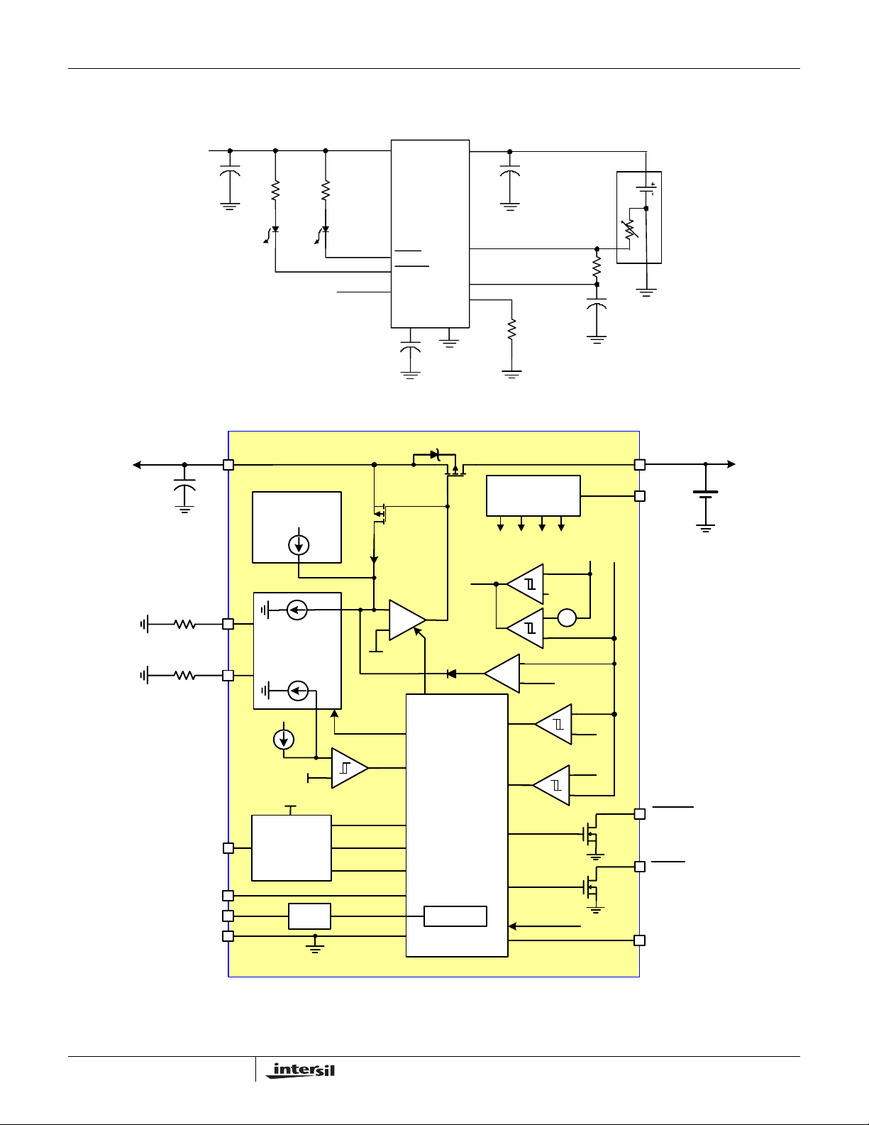
Theory of Operation
-
The ISL6292 is an integrated charger for single-cell Li-ion or
Li-polymer batteries. The ISL6292 functions as a traditional
linear charger when powered with a voltage-source adapter.
When powered with a current-limited adapter, the charger
minimizes the thermal dissipation commonly seen in
traditional linear chargers.
As a linear charger, the ISL6292 charges a battery in the
popular constant current (CC) and constant voltage (CV)
profile. The constant charge current I
to 2A (1.5A for the 3x3 DFN package) with an external resistor
or a logic input. The charge voltage V
over the entire recommended operating condition range. The
charger always preconditions the battery with 10% of the
programmed current at the beginning of a charge cycle, until
the battery voltage is verified to be above the minimum fa st
charge voltage, V
. This low-current preconditioning
MIN
charge mode is named trickle mode. The verification takes 15
cycles of an internal oscillator whose period is programmable
with the timing capacitor. A thermal-foldback feature removes
the thermal concern typically seen in linear chargers. The
charger reduces the charge current automatically as the IC
internal temperature rises above +100°C to prevent further
temperature rise. The thermal-foldback feature guarantees
safe operation when the printed circuit board (PCB) is space
limited for thermal dissipation.
A TEMP pin monitors the battery temperature to ensure a
safe charging temperature range. The temperature range is
programmable with an external negative temperature
coefficient (NTC) thermistor. The TEMP pin is also used to
detect the removal of the battery.
The charger offers a safety timer for setting the fast charge time
(TIMEOUT) limit to prevent charging a dead battery for an
extensively long time. The TIMEOUT limit can be disabled as
needed by the TOEN pin. The trickle mode is limited to 1/8 of
TIMEOUT and cannot be disabled by the TOEN pin.
Trickle
V
IN
V
CH
V
MIN
Constant Current
Mode
Input Voltage
Mode
is programmable up
REF
has 1% accuracy
CH
Constant Voltage
Mode
Battery Voltage
Inhibit
The charger automatically re-charges the battery when the
battery voltage drops below a recharge threshold. When the
wall adapter is not present, the ISL6292 draws less than 1
µA
current from the battery.
Three indication pins are available from the charger to
indicate the charge status. The V2P8 outputs a 2.8VDC
voltage when the input voltage is above the power-on reset
(POR) level and can be used as the power-present
indication. This pin is capable of sourcing a 2mA current, so
it can also be used to bias external circuits. The STATUS pin
is an open-drain logic output that turns LOW at the beginning
of a charge cycle until the end-of-charge (EOC) condition is
qualified. The EOC condition is: the battery voltage rises
above the recharge threshold and the charge current falls
below a user-programmable EOC current threshold. Once
the EOC condition is qualified, the STATUS output rises to
HIGH and is latched. The latch is released at the beginning
of a charge or re-charge cycle. The open-drain FAULT pin
turns low when any fault conditions occur. The fault
conditions include the external battery temperature fault, a
charge time fault, or the battery removal.
Figure 17 shows the typical charge curves in a traditional
linear charger powered with a constant-voltage adapter.
From top to bottom, the curves represent the constant input
voltage, the battery voltage, the charge current and the
power dissipation in the charger. The power dissipation P
CH
is given by Equation 1:
P
CH
where I
VIN-V
()I
BAT
CHARGE
is the charge current. The maximum power
⋅=
CHARGE
(EQ. 1)
dissipation occurs during the beginning of the CC mode. The
maximum power the IC is capable of dissipating is
dependent on the thermal impedance of the printed-circuit
board (PCB). Figure 17 shows (with dotted lines) two cases
that the charge currents are limited by the maximum power
dissipation capability due to the thermal foldback.
V
IN
V
CH
V
MIN
I
REF
Charge Current
I
/10
REF
P
1
P
2
P
3
Power Dissipation
TIMEOUT
FIGURE 17. TYPICAL CHARGE CURVES USING A
CONSTANT-VOLTAGE ADAPTER
10
I
REF
I
LIM
I
/10
REF
P
1
P
2
FIGURE 18. TYPICAL CHARGE CURVES USING A CURRENT
LIMITED ADAPTER
FN9105.9
December 17, 2007
Page 11

ISL6292
When using a current-limited adapter, the thermal situation
in the ISL6292 is totally different. Figure 18 shows the typical
charge curves when a current-limited adapter is employed.
The operation requires the I
than the limited current I
to be programmed higher
REF
of the adapter, as shown in
LIM
Figure 18. The key difference of the charger operating under
such conditions occurs during the CC mode.
The Block Diagram (Figure 16) aids in understanding the
operation. The current loop consists of the current amplifier
CA and the sense MOSFET Q
. The current reference IR
SEN
is programmed by the IREF pin. The current amplifier CA
regulates the gate of the sense MOSFET Q
sensed current I
main MOSFET Q
matches the reference current IR. The
SEN
and the sense MOSFET Q
MAIN
SEN
so that the
form a
SEN
current mirror with a ratio of 100,000:1, that is, the output
charge current is 100,000 times I
. In the CC mode, the
R
current loop tries to increase the charge current by
enhancing the sense MOSFET Q
, so that the sensed
SEN
current matches the reference current. On the other hand,
the adapter current is limited, the actual output current will
never meet what is required by the current reference. As a
result, the current error amplifier CA keeps enhancing the
Q
as well as the main MOSFET Q
SEN
, until they are
MAIN
fully turned on. Therefore, the main MOSFET becomes a
power switch instead of a linear regulation device. The
power dissipation in the CC mode becomes Equation 2:
P
CHrDS ON()ICHARGE
where r
DS(ON)
⋅=
is the resistance when the main MOSFET is
2
(EQ. 2)
fully turned on. This power is typically much less than the
peak power in the traditional linear mode.
The worst power dissipation when using a current-limited
adapter typically occurs at the beginning of the CV mode, as
shown in Figure 18. Equation 1 applies during the CV mode.
When using a very small PCB whose thermal impedance is
relatively large, it is possible that the internal temperature
can still reach the thermal foldback threshold. In that case,
the IC is thermally protected by lowering the charge current,
as shown with the dotted lines in the charge current and
power curves. Appropriate design of the adapter can further
reduce the peak power dissipation of the ISL6292.
See“Applications Information” on page 1 1 for more
information.
Figure 19 illustrates the typical signal waveforms for the
linear charger from the power-up to a recharge cycle. More
detailed Applications Information is given in the following.
Applications Information
The two indication pins, STATUS and FAULT, indicate a
LOW and a HIGH logic signal respectively. Figure 19
illustrates the start-up of the charger between t
to t2.
0
The ISL6292 has a typical rising POR threshold of 3.4V and
a falling POR threshold of 2.4V. The 2.4V falling threshold
guarantees charger operation with a current-limited adapter
to minimize the thermal dissipation.
Charge Cycle
A charge cycle consists of three charge modes: trickle mode,
constant current (CC) mode, and constant volt age (CV) mode.
The charge cycle always starts with the trickle mode until the
battery voltage stays above V
consecutive cycles of the internal oscillator. If the battery
voltage drops below V
MIN
counter is reset and the charger stays in the trickle mode. The
charger moves to the CC mode after verifying the battery
voltage. As the battery-pack terminal voltage rises to the final
charge voltage V
, the CV mode begins. The terminal
CH
voltage is regulated at the constant V
the charge current is expected to decline. After the charge
current drops below I
(programmable for the 4x4 and 5x5
MIN
package and programmed to 1/10 of I
package; see “End-of-Charge (EOC) Current” on page13 for
more detail), the ISL6292 indicates the end-of-charge (EOC)
with the STA TUS pin. The charging actu ally does not
terminate until the internal timer completes its length of
TIMEOUT in order to bring the battery to its full capacity.
Signals in a charge cycle are illustrated in Figure 19 between
points t
VIN
V2P8
STATUS
FAULT
VBAT
I
CHARGE
to t5.
2
POR Threshold
Charge Cycle
15 Cycles to
1/8 TIMEOUT
2.8V V
t0t1t2t
FIGURE 19. OPERATION WAVEFORMS
t
3
(2.8V typical) for 15
MIN
during the 15 cycles, the 15-cycle
in the CV mode and
CH
for the 3x3
REF
Charge Cycle
V
RECHRG
MIN
I
MIN
4
t
5t6t7
15 Cycles
t
8
Power on Reset (POR)
The ISL6292 resets itself as the input voltage rises above
the POR rising threshold. The V2P8 pin outputs a 2.8V
voltage, the internal oscillator starts to oscillate, the internal
timer is reset, and the charger begins to charge the battery.
11
FN9105.9
December 17, 2007
Page 12

ISL6292
The following events initiate a new charge cycle:
•POR,
• a new battery being inserted (detected by TEMP pin),
• the battery voltage drops below a recharge threshold after
completing a charge cycle,
• recovery from an battery over-temperature fault,
• or, the EN pin is toggled from GND to floating.
Further description of these events are given later in this
data sheet.
Recharge
After a charge cycle completes, charging is prohibited until
the battery voltage drops to a recharge threshold, V
RECHRG
(see “Electrical Specifications” on page 3). Then a new
charge cycle starts at point t
in Figure 19. The safety timer is reset at t
and ends at point t8, as shown
6
.
6
Internal Oscillator
The internal oscillator establishes a timing reference. The
oscillation period is programmable with an external timing
capacitor , C
, as shown in Typical Applications. The
TIME
oscillator charges the timing capacitor to 1.5V and then
discharges it to 0.5V in one period, both with 10µA current.
The period t
t
OSC
0.2 106C
is:
OSC
⋅⋅= ondssec()
TIME
(EQ. 3)
A 1nF capacitor results in a 0.2ms oscillation period. The
accuracy of the period is mainly dependent on the accuracy
of the capacitance and the internal current source.
Total Charge Time
The total charge time for the CC mode and CV mode is
limited to a length of TIMEOUT. A 22-stage binary counter
increments each oscillation period of the internal oscillator to
set the TIMEOUT. The TIMEOUT can be calculated as:
TIMEOUT 2
22
t
OSC
A 1nF capacitor leads to 14 minutes of TIMEOUT. For
example, a 15nF capacitor sets the TIMEOUT to be
3.5 hours. The charger has to reach the end-of-charge
condition before the TIMEOUT, otherwise, a TIMEOUT fault
is issued. The TIMEOUT fault latches up the charger. There
are two ways to release such a latch-up: either to recycle the
input power, or toggle the EN pin to disable the charger and
then enable it again.
The trickle mode charge has a time limit of 1/8 TIMEOUT. If
the battery voltage does not reach V
TIMEOUT fault is issued and the charger latches up. The
charger stays in trickle mode for at least 15 cycles of the
internal oscillator and, at most, 1/8 of TIMEOUT, as shown in
Figure 19.
C
TIME
------------------
14
⋅=⋅= minutes()
1nF
within this limit, a
MIN
(EQ. 4)
Disabling TIMEOUT Limit
The TIMEOUT limit for the fast charge modes can be disabled
by pulling the TOEN pin to LOW or shorting it to GND. When
this happens, the charger becomes a current-limited LDO
(low-dropout) supply with its voltage regulated at the fi nal
charge voltage V
and the current limit determined by the
CH
IREF pin. If the LDO load current drops below the end-ofcharge current (refer to “End-of-Charge (EOC) Current” on
page 13), the STATUS pin will indicate.
The trickle charge time limit, however, is not disabled even
when the TOEN pin is pulled to LOW. The charger operates
in the trickle mode at the beginning of a charge cycle even if
the TIMEOUT is disabled. Leaving the TOEN pin floating is
recommended to enable the TIMEOUT. Driving the TOEN
pin above 3.0V is not recommended.
Charge Current Programming
The charge current is programmed by the IREF pin. There
are three ways to program the charge current:
1. Driving the IREF pin above 1.3V
2. Driving the IREF pin below 0.4V,
3. or using the R
page 8.
The voltage of IREF is regulated to a 0.8V reference voltage
when not driven by any external source. The charging
current during the constant current mode is 100,000 times
that of the current in the R
on how IREF pin is used, the charge current is:
⎧
500mA
⎪
⎪
0.8V
I
REF
-----------------
=
⎨
R
⎪
IREF
⎪
100mA
⎩
The 500mA current is a guaranteed maximum value for the
high-power USB port, with the typical value of 450mA. The
100mA current is also a guaranteed maximum value for the
low-power USB port. This design accommodates the USB
power specification.
The internal reference voltage at the IREF pin is capable of
sourcing less than 100µA current. When pulling down the
IREF pin with a logic circuit, the logic circuit needs to be able
to sink at least 100µA current.
When the adapter is current limited, it is recommended that
the reference current be programmed to at least 30% higher
than the adapter current limit (which equals the charge
current). In addition, the charge current should be at least
350mA so that the voltage difference between the VIN and
the VBAT pins is higher than 100mV. The 100mV is the
offset voltage of the input-output voltage comparator shown
in the block diagram on page 9.
as shown in “Typical Applications” on
IREF
resistor. Hence, depending
IREF
IREF
IREF
IREF
1.3V>
0.4V<
5
× A()
10
V
R
V
(EQ. 5)
12
FN9105.9
December 17, 2007
Page 13

ISL6292
End-of-Charge (EOC) Current
The end-of-charge current I
charger starts to indicate the end of the charge with the
STATUS pin, as shown in Figure 19. The charger actually
does not terminate charging until the end of the TIMEOUT,
as described in “Total Charge Time” on page 12. The I
set in two ways, by connecting a resistor between the IMIN
pin and ground, or by connecting the IMIN pin to the V2P8
pin. When programming with the resistor, the I
Equation 6.
I
MIN
where R
----------------
10000
R
is the resistor connected between the IMIN pin
IMIN
IMIN
---------------R
V
REF
and the ground. When connected to the V2P8 pin, the I
is set to 1/10 of I
, except when the IREF pin is shorted to
REF
GND. Under this exception, I
the 3x3 DFN package, the IMIN pin is bonded internally to
V2P8.
sets the level at which the
MIN
IMIN
4
×10
A()=⋅=
is 5mA. For the ISL6292 in
MIN
0.8V
MIN
MIN
is set in
(EQ. 6)
MIN
is
Charge Current Thermal Foldback
Over-heating is always a concern in a linear charger. The
maximum power dissipation usually occurs at the beginning
of a charge cycle when the battery voltage is at its minimum
but the charge current is at its maximum. The charge current
thermal foldback function in the ISL6292 frees users from
the over-heating concern.
Figure 20 shows the current signals at the summing node of
the current error amplifier CA in the Block Diagram shown on
page 9. I
Temperature Monitoring block. The I
charge current until the internal temperature reaches
approximately +100°C; then I
When I
current I
current, the charge current is 100,000 times that of the
sensed current and reduces at a rate of 100mA/°C. For a
charger with the constant charge current set at 1A, the
charge current is reduced to zero when the internal
temperature rises to +110°C. The actual charge current
settles between +100°C to +110°C.
is the reference and IT is the current from the
R
T
rises, the current control loop forces the sensed
T
to reduce at the same rate. As a mirrored
SEN
has no impact on the
T
rises at a rate of 1µA/°C.
I
R
2.8V Bias Voltage
The ISL6292 provides a 2.8V voltage for biasing the internal
control and logic circuit. This voltage is also available for
external circuits such as the NTC thermistor circuit. The
maximum allowed external load is 2mA.
NTC Thermistor
The ISL6292 uses two comparators (CP2 and CP3) to form a
window comparator , as shown in Figure 22.
pin voltage is “out of the window,” determined by the V
and V
, the ISL6292 stops charging and indicates a fault
TMAX
condition. When the temperature returns to th e set range, the
charger re-starts a charge cycle. The two MOSFETs, Q1 and
Q2, produce hysteresis for both upper and lower thresholds.
The temperature window is shown in Figure 21.
2.8V
(1.4V)
V
TMIN
V
(1.2V)
TMIN-
V
(0.406V)
TMAX+
V
(0.35V)
TMAX
0V
Under
Temp
Over
Temp
FIGURE 21. CRITICAL VOLTAGE LEVELS FOR TEMP PIN
ISL6292
Battery
Removal
Under
Temp
CP1
CP2
V
RMV
-
+
V
-
+
TMIN
To TEMP Pin
Q1
When the TEMP
2.8V
R1
40K
R2
60K
R3
75K
V2P8
TEMP
TMIN
TEMP
Pin
Voltage
R
U
I
T
I
SEN
Temperature100OC
FIGURE 20. CURRENT SIGNALS A T THE AMPLIFI ER CA INPUT
Usually the charge current should not drop below I
because
MIN
of the thermal foldback. For some extreme cases (if that does
happen) the charger does not indicate end-of-charge unless
the battery voltage is already above the recharge threshold.
13
Over
Temp
CP3
-
V
TMAX
+
R4
25K
Q2
R5
4K
GND
R
T
FIGURE 22. THE INTERNAL AND EXTERNAL CIRCUIT FOR
THE NTC INTERFACE
As the TEMP pin voltage rises from low and exceeds the 1.4V
threshold, the under temperature signal rises and does not
clear until the TEMP pin voltage falls below the 1.2V falling
threshold. Similarly, the over-temperature signal is given when
the TEMP pin voltage falls below the 0.35V threshold and does
FN9105.9
December 17, 2007
Page 14

ISL6292
not clear until the voltage rises above 0.406V. The actual
accuracy of the 2.8V is not important because all the
thresholds and the TEMP pin voltage are ratios determined by
the resistor dividers, as shown in Figure 22.
The NTC thermistor is required to have a resistance ratio of
7:1 at the low and the high temperature limits, that is:
R
COLD
--------------------
R
HOT
7=
(EQ. 7)
This is because at the low temperature li mit, the TEMP pin
voltage is 1.4V, which is 1/2 of the 2.8V bias. Thus:
R
where R
=
COLDRU
is the pull-up resistor as shown in Figure 22. On
U
(EQ. 8)
the other hand, at the high temperature limit the TEMP pin
voltage is 0.35V, 1/8 of the 2.8V bias. Therefore:
R
HOT
U
------- -
=
7
(EQ. 9)
R
Various NTC thermistors are available for this application.
Table 1 shows the resistance ratio and the negative
temperature coefficient of the curve-1 NTC thermistor from
Vishay (http://www.vishay .com) at various temperatures. The
resistance at +3°C is approximately seven times the
resistance at +47°C, which is shown in Equation 10:
R
3° C
---------------- -
R
47° C
7=
(EQ. 10)
Therefore, if +3°C is the low temperature limit, then the high
temperature limit is approximately +47°C. The pull-up resistor
R
can choose the same value as the resistance at +3°C.
U
TABLE 1. RESISTANCE RATIO OF VISHAY’S CURVE-1 NTC
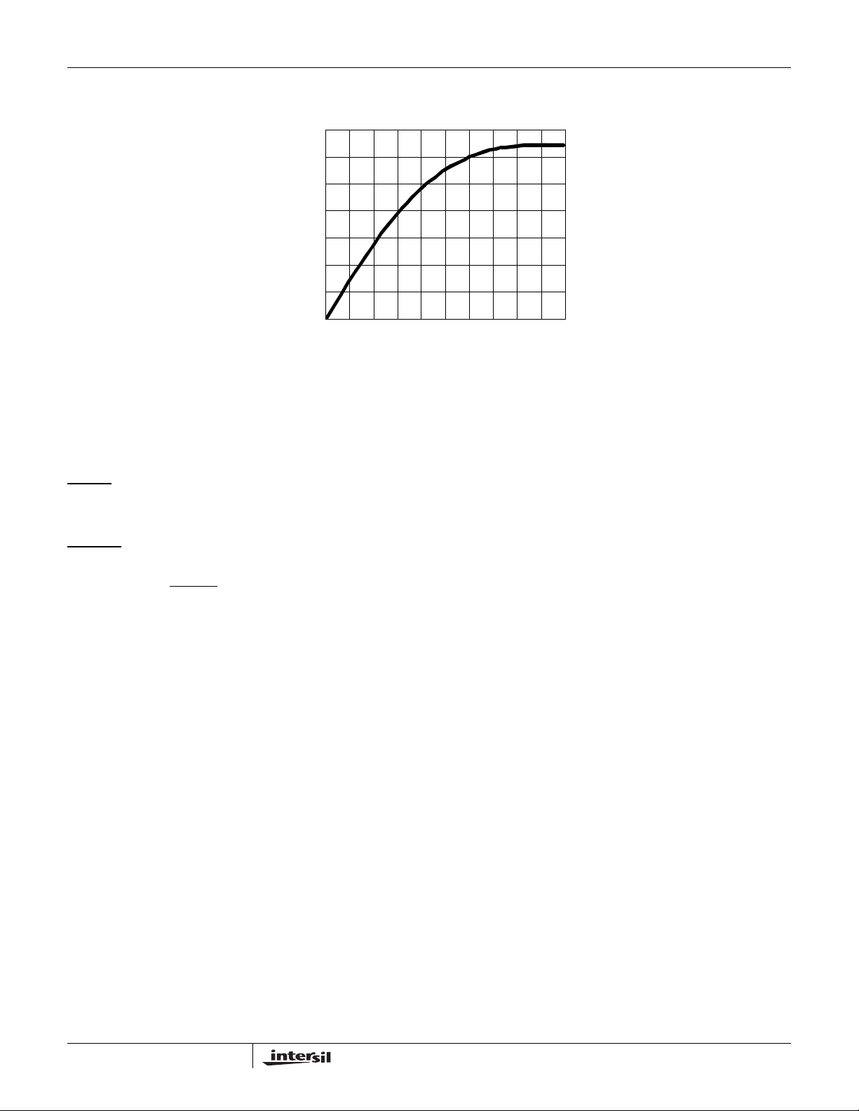
TEMPERATURE (°C) RT/R
0 3.266 5.1
3 2.806 5.1
5 2.540 5.0
25 1.000 4.4
45 0.4368 4.0
47 0.4041 3.9
50 0.3602 3.9
25°C
NTC (%/°C)
The temperature hysteresis can be estimated. At the low
temperature, the hysteresis is approximately estimated in
Equation 11:
T
hysLOW
--------------------------------
1.4V 0.051⋅
()
3≈≈°
C
(EQ. 11)
1.4V-1.2V
where 0.051 is the NTC at +3°C. Similarly, the high
temperature hysteresis is estimated in Equation 12:
T
hysHIGH
--------------------------------------
0.35V 0.039⋅
()
4≈≈°
C
(EQ. 12)
0.406V-0.35V
where the 0.039 is the NTC at +47°C.
For applications that do not need to monitor the battery
temperature, the NTC thermistor can be replaced with a
regular resistor of a half value of the pull-up resistor R
.
U
Another option is to connect the TEMP pin to the IREF pin
that has a 0.8V output. With such connection, the IREF pin
can no longer be programmed with logic inputs.
Battery Removal Detection
The ISL6292 assumes that the thermistor is co-packed with
the battery and is removed together with the battery. When
the charger senses a TEMP pin voltage that is 2.1V or
higher, it assumes that the battery is removed. The battery
removal detection circuit is also shown in Figure 22. When a
battery is removed, a FAULT signal is indicated and charging
is halted. When a battery is inserted again, a new charge
cycle starts.
Indications
The ISL6292 has three indications: the input presence, the
charge status, and the fault indication. The input presence is
indicated by the V2P8 pin while the other two indications are
presented by the STATUS pin and FAULT pin respectively.
Figure 23 shows the V2P8 pin voltage vs the input voltage.
Table 2 summarizes the other two pins.
3.4V
2.4V
2.8V
V
IN
V2P8
FIGURE 23. THE V2P8 PIN OUTPUT vs THE INPUT VOLTAGE
AT THE VIN PIN. VERTICAL: 1V/DIV,
HORIZONTAL: 100ms/DIV
Shutdown
The ISL6292 can be shutdown by pulling the EN pin to
ground. When shut down, the charger draws typically less
than 30µA current from the input power and the 2.8V output
at the V2P8 pin is also turned off. The EN pin needs to be
driven with an open-drain or open-collector logic output, so
that the EN pin is floating when the charger is enabled.
TABLE 2. STATUS INDICATIONS
FAULT STATUS INDICATION
High High Charge completed with no fault (Inhibit) or
Standby
*Both outputs are pulled up with external resistors.
14
FN9105.9
December 17, 2007
Page 15

ISL6292
TABLE 2. STATUS INDICATIONS
FAULT STATUS INDICATION
High Low Charging in one of the three modes
Low High Fault
*Both outputs are pulled up with external resistors.
Input and Output Capacitor Selection
Typically any type of capacitors can be used for the input
and the output. Use of a 0.47µF or higher value ceramic
capacitor for the input is recommended. When the battery is
attached to the charger, the output capacitor can be any
ceramic type with the value higher than 0.1µF. However, if
there is a chance the charger will be used as an LDO linear
regulator, a 10µF tantalum capacitor is recommended.
Current-Limited Adapter
Figure 24 shows the ideal current-voltage characteristics of
a current-limited adapter. V
voltage and V
I
. Before its output current reaches the limit I
LIM
is the full load voltage at the current limit
FL
adapter presents the characteristics of a voltage source. The
slope r
represents the output resistance of the voltage
O
supply. For a well regulated supply, the output resistance
can be very small, but some adapters naturally have a
certain amount of output resistance.
The adapter is equivalent to a current source when running
in the constant-current region. Being a current source, its
output voltage is dependent on the load, which, in this case,
is the charger and the battery. As the battery is being
charged, the adapter output rises from a lower voltage in the
current-voltage characteristics curve, such as point A, to
higher voltage until reaching the breaking point B, as shown
in Figure 24.
The adapter is equivalent to a voltage source with output
resistance when running in the constant-voltage region;
because of this characteristic. As the charge current drops,
the adapter output moves from point B to point C, shown in
Figure 24.
The battery pack can be approximated as an ideal cell with a
lumped-sum resistance in series, also shown in Figure 24.
The ISL6292 charger sits between the adapter and the
battery.
V
NL
V
FL
FIGURE 24. THE IDEAL I-V CHARACTERISTICS OF A
C
r
O
V
NL
CURRENT LIMITED ADAPTER
is the no-load adapter output
NL
LIM
- VFL)/I
(V
rO =
NL
LIM
B
I
LIM
V
CELL
A
I
LIM
, the
V
R
PACK
PACK
Working with Current-Limited Adapter
As described earlier, the ISL6292 minimizes the thermal
dissipation when running off a current-limited AC adapter, as
shown in Figure 18. The thermal dissipation can be further
reduced when the adapter is properly designed. The
following demonstrates that the thermal dissipation can be
minimized if the adapter output reaches the full-load output
voltage (point B in Figure 24) before the battery pack voltage
reaches the final charge voltage (4.1V or 4.2V). The
assumptions for the following discussion are: the adapter
current limit = 750mA, the battery pack equivalent
resistance = 200mΩ, and the charger ON-resistance is
350mΩ.
When charging in the constant-current region, the pass
element in the charger is fully turned on. The charger is
equivalent to the ON-resistance of the internal P-Channel
MOSFET. The entire charging system is equivalent to the
circuit shown in Figure 25A. The charge current is the
constant current limit I
can be easily found out as calculated in Equation 13:
V
AdapterILIM
where V
PACK
r
DS ON()
is the battery pack voltage. The power
dissipation in the charger is given in Equation 2, where
I
CHARGE
= I
LIM
.
A critical condition of the adapter design is that the adapter
output reaches point B in Figure 24 at the same time as the
battery pack voltage reaches the final charge voltage (4.1V
or 4.2V), that is:
V
CriticalILIM
r
DS ON()
For example, if the final charge voltage is 4.2V, the r
is 350mΩ, and the current limit I
adapter full-load voltage is 4.4625V.
When the above condition is true, the charger enters the
constant-voltage mode simultaneously as the adapter exits
the current-limit mode. The equivalent charging system is
shown in Figure 25C. Since the charge current drops at a
higher rate in the constant-voltage mode than the increase
rate of the adapter voltage, the power dissipation decreases
as the charge current decreases. Therefore, the worst case
thermal dissipation occurs in the constant-current charge
mode. Figure 25A shows the I-V curves of the adapter
output, the battery pack voltage and the cell voltage during
the charge. The 5.9V no-load voltage is just an example
value higher than the full-load voltage. The cell voltage
4.05V uses the assumption that the pack resistance is
200mΩ. Figure 26A illustrates the adapter voltage, battery
pack voltage, the charge current and the power dissipation in
the charger respectively in the time domain.
, and the adapter output voltage
LIM
V
+⋅=
PACK
VCH+⋅=
is 750mA, the critical
LIM
(EQ. 13)
(EQ. 14)
DS(ON)
15
FN9105.9
December 17, 2007
Page 16
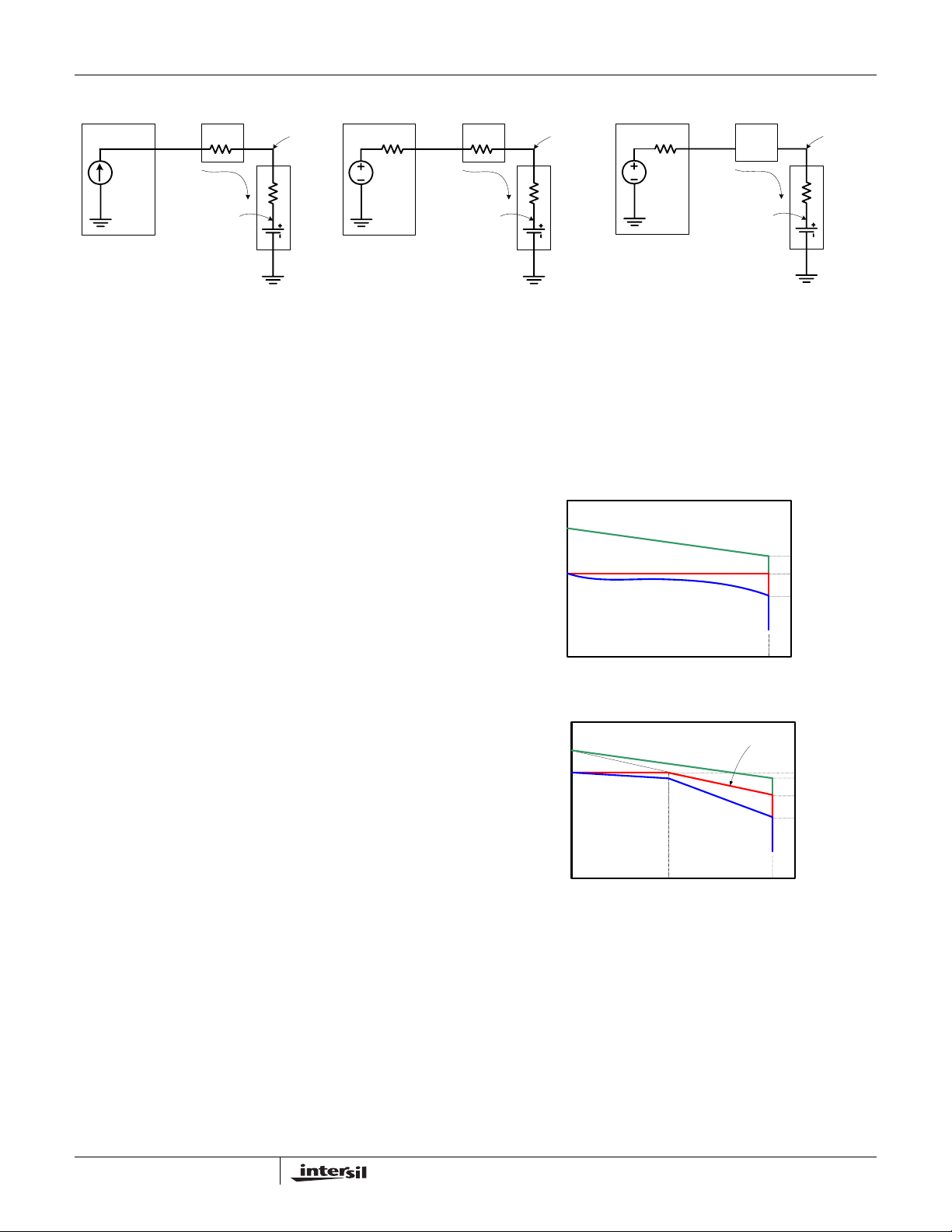
ISL6292
Adapter
I
LIM
V
ADAPTER
Charger
R
DS(ON)
V
CELL
V
PACK
I
R
PACK
Battery
Pack
FIGURE 25A. THE EQUIVALENT CIRCUIT IN
THE CONSTANT CURRENT
REGION
Adapter
V
r
O
V
NL
FIGURE 25B. THE EQUIVALENT CIRCUIT IN
THE RESISTANCE-LIMIT
REGION
FIGURE 25. THE EQUIVALENT CIRCUIT OF THE CHARGING SYSTEM WORKING WITH CURRENT LIMITED ADAPTERS
If the battery pack voltage reaches 4.2V (or 4.1V) before the
adapter reaches point B in Figure 24, a voltage step is
expected at the adapter output when the pack voltage
reaches the final charge voltage. As a result, the charger
power dissipation is also expected to have a step rise. This
case is shown in Figure 18 as well as Figure 27C. Under this
condition, the worst case thermal dissipation in the charger
happens when the charger enters the constant voltage
mode.
If the adapter voltage reaches the full-load voltage before the
pack voltage reaches 4.2V (or 4.1V), the charger will
experience the resistance-limit situation. In this situation, the
ON-resistance of the charger is in series with the adapter
output resistance. The equivalent circuit for the resistance-limit
region is shown in Figure 25B. Eventually, the battery pack
voltage will reach 4.2V (or 4.1V) because the adapter no-load
voltage is higher than 4.2V (or 4.1V), then Figure 25C becomes
the equivalent circuit until charging ends. In this case, the
worst-case thermal dissipation also occurs in the constantcurrent charge mode. Figure 26B shows the I-V curves of the
adapter output, the battery pack voltage and the cell voltage for
the case V
= 4V . In the case, the full-load voltage is lower
FL
than the final charge voltage (4.2V), but the charger is still able
to fully charge the battery as long as the no-load voltage is
above 4.2V . Figure 26B illustrates the adapter voltage, battery
pack v ol tage, the charge current and the power dissipation in
the charger respectively in the time domain.
Based on the previous discussion, the worst-case power
dissipation occurs during the constant-current charge mode
if the adapter full-load voltage is lower than the critical
voltage given in Equation 14. Even if that is not true, the
power dissipation is still much less than the power
dissipation in the traditional linear charger. Figures 28 and
29 are scope-captured waveforms to demonstrate the
operation with a current-limited adapter.
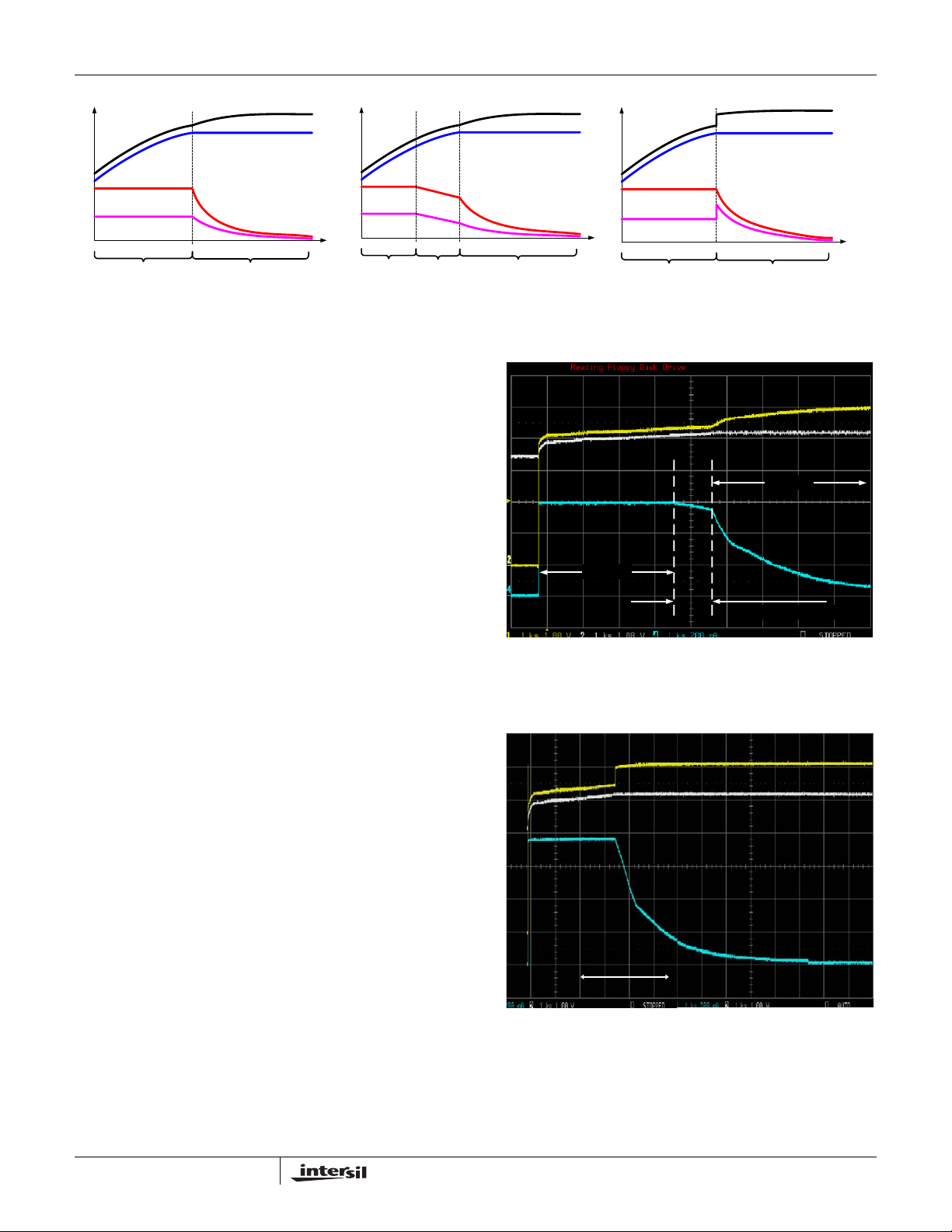
The waveforms in Figure 28 are the adapter output voltage
(1V/div), the battery voltage (1V/div), and the charge current
(200mA/div) respectively. The time scale is 1ks/div. The
ADAPTER
Charger
R
DS(ON)
V
CELL
Adapter
V
PACK
I
R
PACK
Battery
Pack
r
O
V
NL
V
ADAPTER
Charger
4.2V DC
Output
V
CELL
I
FIGURE 25C. THE EQUIVALENT CIRCUIT WHEN
THE PACK VOLTAGE REACHES
THE FINAL CHARGE VOLTAGE
adapter current is limited to 600mA and the charge current is
programmed to 1A. Note that the voltage difference is only
approximately 200mV and the adapter voltage tracks the
battery voltage in the CC mode. Figure 28 also shows the
resistance-limit mode before entering the CV mode.
5.9V
4.2V
V
NL
4.2V
FIGURE 26. THE I-V CHARACTERISTICS OF THE CHARGER
WITH DIFFERENT CURRENT LIMITED ADAPTERS
V
ADAPTER
V
PACK
V
CELL
FIGURE 26A.
V
ADAPTER
V
CELL
0.55A
FIGURE 26B.
0.75A
V
PACK
0.75A
Figure 29 shows the actual captured waveforms depicted in
Figure 27C. The constant charge current is 750mA. A step in
the adapter voltage during the transition from CC mode to
CV mode is demonstrated.
V
4.4625V
4.2V
4.05V
4.2V
4.0V
3.775V
3.625V
PACK
R
PACK
Battery
Pack
16
FN9105.9
December 17, 2007
Page 17
ISL6292
V
IN
V
PACK
V
IN
V
PACK
V
IN
V
PACK
Charge
Current
Power
Const. Cur
TIME
Constant Voltage
Power
Const. Cur
Res
Limit
FIGURE 27A.
FIGURE 27. THE OPERATING CURVES WITH THREE DIFFERENT CURRENT LIMITED ADAPTERS
IREF Programming Using Current-Limited Adapter
The ISL6292 has 10% tolerance for the charge current.
Typically the current-limited adapter also has 10% tolerance.
In order to guarantee proper operation, it is recommended
that the nominal charge current be programmed at least
30% higher than the nominal current limit of the adapter.
Board Layout Recommendations
The ISL6292 internal thermal foldback function limits the
charge current when the internal temperature reaches
approximately +100°C. In order to maximize the current
capability , it is very important that the exposed pad under the
package is properly soldered to the board and is connected
to other layers through thermal vias. More thermal vias and
more copper attached to the exposed pad usually result in
better thermal performance. On the other hand, the number
of vias is limited by the size of the pad. The exposed pads for
the 5x5 and 4x4 QFN packages are able to have 9 and 5
vias respectively. The 3x3 DFN package allows 8 vias be
placed in two rows. Since the pins on the 3x3 DFN package
are on only two sides, as much top layer copper as possible
should be connected to the exposed pad to minimize the
thermal impedance. Refer to the ISL6292 evaluation boards
for layout examples.
Charge
Current
Constant Voltage
FIGURE 27B.
Charge
Current
Power
TIME
Const. Cur
Constant Voltage
TIME
FIGURE 27C.
CV Mode
CC Mode
Resistance Limit Mode
FIGURE 28. SCOPE CAPTURED WA VEFORMS SHOWING THE
THREE MODES
17
1 hour
FIGURE 29. SCOPE CAPTURED WA VEFORMS SHOWING THE
CASE THAT THE FULL-LOAD ADAPTER
VOLTAGE IS HIGHER THAN THE CRITICAL
VOLTAGE
FN9105.9
December 17, 2007
Page 18

Dual Flat No-Lead Plastic Package (DFN)
ISL6292
INDEX
SEATING
(DATUM B)
6
INDEX
AREA
(DATUM A)
NX (b)
5
SECTION "C-C"
6
AREA
C
PLANE
NX L
8
A
12
D
TOP VIEW
SIDE VIEW
8
7
D2
D2/2
N-1N
e
(Nd-1)Xe
REF.
BOTTOM VIEW
(A1)
2X
A3
NX b
5
0.415
0.15
C
E
B
A
NX
E2
E2/2
0.10 MC
0.200
NX b
C
A
0.152XB
0.10 C
C
0.08
k
AB
NX L
L10.3x3
10 LEAD DUAL FLAT NO-LEAD PLASTIC PACKAGE
MILLIMETERS
C
SYMBOL
NOTESMIN NOMINAL MAX
A 0.80 0.90 1.00 A1 - - 0.05 A3 0.20 REF -
b 0.18 0.23 0.28 5,8
D 3.00 BSC -
D2 1.95 2.00 2.05 7,8
E 3.00 BSC -
E2 1.55 1.60 1.65 7,8
e 0.50 BSC -
k 0.25 ---
L 0.30 0.35 0.40 8
N102
Nd 5 3
Rev. 3 6/04
NOTES:
1. Dimensioning and tolerancing conform to ASME Y14.5-1994.
2. N is the number of terminals.
3. Nd refers to the number of terminals on D.
4. All dimensions are in millimeters. Angles are in degrees.
5. Dimension b applies to the metallized terminal and is measured
between 0.15mm and 0.30mm from the terminal tip.
6. The configuration of the pin #1 identifier is optional, but must be
located within the zone indicated. The pin #1 identifier may be
either a mold or mark feature.
7. Dimensions D2 and E2 are for the exposed pads which provide
improved electrical and thermal performance.
8. Nominal dimensions are provided to assist with PCB Land
Pattern Design efforts, see Intersil Technical Brief TB389.
C
L
L
e
CC
FOR ODD TERMINAL/SIDE
TERMINAL TIP
18
FN9105.9
December 17, 2007
Page 19

ISL6292
Quad Flat No-Lead Plastic Package (QFN)
Micro Lead Frame Plastic Package (MLFP)
L16.4x4
16 LEAD QUAD FLAT NO-LEAD PLASTIC PACKAGE
(COMPLIANT TO JEDEC MO-220-VGGC ISSUE C)
MILLIMETERS
SYMBOL
A 0.80 0.90 1.00 A1 - - 0.05 A2 - - 1.00 9
A3 0.20 REF 9
b 0.23 0.28 0.35 5, 8
D 4.00 BSC D1 3.75 BSC 9
D2 1.95 2.10 2.25 7, 8
E 4.00 BSC E1 3.75 BSC 9
E2 1.95 2.10 2.25 7, 8
e 0.65 BSC -
k0.25 - - -
L 0.50 0.60 0.75 8
L1 - - 0.15 10
N162
Nd 4 3
Ne 4 3
P- -0.609
θ --129
NOTES:
1. Dimensioning and tolerancing conform to ASME Y14.5-1994.
2. N is the number of terminals.
3. Nd and Ne refer to the number of terminals on each D and E.
4. All dimensions are in millimeters. Angles are in degrees.
5. Dimension b applies to the metallized terminal and is measured
between 0.15mm and 0.30mm from the terminal tip.
6. The configuration of the pin #1 identifier is optional, but must be
located within the zone indicated. The pin #1 identifier may be
either a mold or mark feature.
7. Dimensions D2 and E2 are for the exposed pads which provide
improved electrical and thermal performance.
8. Nominal dimensions are provided to assist with PCB Land Pattern
Design efforts, see Intersil Technical Brief TB389.
9. Features and dimensions A2, A3, D1, E1, P & θ are present when
Anvil singulation method is used and not present for saw
singulation.
10. Depending on the method of lead termination at the edge of the
package, a maximum 0.15mm pull back (L1) maybe present. L
minus L1 to be equal to or greater than 0.3mm.
NOTESMIN NOMINAL MAX
Rev. 5 5/04
19
FN9105.9
December 17, 2007
Page 20

ISL6292
Quad Flat No-Lead Plastic Package (QFN)
Micro Lead Frame Plastic Package (MLFP)
L16.5x5B
16 LEAD QUAD FLAT NO-LEAD PLASTIC PACKAGE
(COMPLIANT TO JEDEC MO-220VHHB ISSUE C)
MILLIMETERS
SYMBOL
A 0.80 0.90 1.00 A1 - - 0.05 A2 - - 1.00 9
A3 0.20 REF 9
b 0.28 0.33 0.40 5, 8
D 5.00 BSC D1 4.75 BSC 9
D2 2.95 3.10 3.25 7, 8
E 5.00 BSC E1 4.75 BSC 9
E2 2.95 3.10 3.25 7, 8
e 0.80 BSC k0.25--L 0.35 0.60 0.75 8
L1 - - 0.15 10
N162
Nd 4 3
Ne 4 3
P--0.609
θ --129
NOTES:
1. Dimensioning and tolerancing conform to ASME Y14.5-1994.
2. N is the number of terminals.
3. Nd and Ne refer to the number of terminals on each D and E.
4. All dimensions are in millimeters. Angles are in degrees.
5. Dimension b applies to the metallized terminal and is measured
between 0.15mm and 0.30mm from the terminal tip.
6. The configuration of the pin #1 identifier is optional, but must be
located within the zone indicated. The pin #1 identifier may be
either a mold or mark feature.
7. Dimensions D2 and E2 are for the exposed pads which provide
improved electrical and thermal performance.
8. Nominal dimensions are provided to assist with PCB Land Pattern
Design efforts, see Intersil Technical Brief TB389.
9. Features and dimensions A2, A3, D1, E1, P & θ are present when
Anvil singulation method is used and not present for saw
singulation.
10. Depending on the method of lead termination at the edge of the
package, a maximum 0.15mm pull back (L1) maybe present. L
minus L1 to be equal to or greater than 0.3mm.
NOTESMIN NOMINAL MAX
Rev. 1 10/02
All Intersil U.S. products are manufactured, assembled and tested utilizing ISO9000 quality systems.
Intersil Corporation’s quality certifications can be viewed at www.intersil.com/design/quality
Intersil products are sold by description only. Intersil Corporation reserves the right to make changes in circuit design, software and/or specifications at any time without
notice. Accordingly, the reader is cautioned to verify that data sheets are current before placing orders. Information furnished by Intersil is believed to be accurate and
reliable. However, no responsibility is assumed by Intersil or its subsidiaries for its use; nor for any infringements of patents or other rights of third parties which may result
from its use. No license is granted by implicat ion or oth erwise u nde r any p a tent or p at ent r ights of Intersil or its subsidiaries.
For information regarding Intersil Corporation and its products, see www.intersil.com
20
FN9105.9
December 17, 2007
 Loading...