


Multiphase PWM Regulator for IMVP-6.5™ Mobile
CPUs and GPUs
ISL62883C
ISL62883C
The ISL62883C is a multiphase PWM buck regulator for
miroprocessor or graphics processor core power supply.
The multiphase buck converter uses interleaved phase to
reduce the total output voltage ripple with each phase
carrying a portion of the total load current, providing
better system performance, superior thermal
management, lower component cost, reduced power
dissipation, and smaller implementation area. The
ISL62883C uses two integrated gate drivers and an
external gate driver to provide a complete solution. The
PWM modulator is based on Intersil's Robust Ripple
Regulator (R
modulators, the R3™ modulator commands variable
switching frequency during load transients, achieving
faster transient response. With the same modulator, the
switching frequency is reduced at light load, increasing
the regulator efficiency.
The ISL62883C can be configured as CPU or graphics
Vcore controller and is fully compliant with IMVP-6.5™
specifications. It responds to PSI# and DPRSLPVR signals
by adding or dropping PWM3 and Phase 2 respectively,
adjusting overcurrent protection threshold accordingly,
and entering/exiting diode emulation mode. It reports
the regulator output current through the IMON pin. It
senses the current by using either discrete resistor or
inductor DCR whose variation over temperature can be
thermally compensated by a single NTC thermistor. It
uses differential remote voltage sensing to accurately
regulate the processor die voltage. The adaptive body
diode conduction time reduction function minimizes
the body diode conduction loss in diode emulation
mode. User-selectable overshoot reduction function
offers an option to aggressively reduce the output
capacitors as well as the option to disable it for users
concerned about increased system thermal stress. In
2-Phase configuration, the ISL62883C offers the FB2
function to optimize 1-Phase performance.
3
) technology™. Compared with traditional
Features
• Programmable 1, 2- or 3-Phase CPU or GPU Mode of
Operation
• Precision Multiphase Core Voltage Regulation
- 0.5% System Accuracy Over-Temperature
- Enhanced Load Line Accuracy
• Microprocessor Voltage Identification Input
- 7-Bit VID Input, 0V to 1.500V in 12.5mV Steps
- Supports VID Changes On-The-Fly
• Supports Multiple Current Sensing Methods
- Lossless Inductor DCR Current Sensing
- Precision Resistor Current Sensing
• Supports PSI# and DPRSLPVR modes
• Superior Noise Immunity and Transient Response
• Current Monitor and Thermal Monitor
• Differential Remote Voltage Sensing
• High Efficiency Across Entire Load Range
• Two Integrated Gate Drivers
• Excellent Dynamic Current Balance
• FB2 Function Optimizes 1-Phase Mode Performance
• Adaptive Body Diode Conduction Time Reduction
• User-selectable Overshoot Reduction Function
• Small Footprint 40 Ld 5x5 TQFN Packages
• Pb-Free (RoHS Compliant)
Applications*(see page 42)
• Notebook Core Voltage Regulator
• Notebook GPU Voltage Regulator
Related Literature*(see page 42)
•See AN1460 for ISL62883/ISL62883C Evaluation
Board Application Note “ISL62883EVAL2Z User
Guide”
Load Line Regulation
(V)
OUT
V
March 18, 2010
FN7557.1
1
1.10
1.08
1.06
1.04
1.02
1.00
0.98
0.96
0.94
0.92
0 5 10 15 20 25 30 35 40 45 50 55 60 65
CAUTION: These devices are sensitive to electrostatic discharge; follow proper IC Handling Procedures.
1-888-INTERSIL or 1-888-468-3774
VIN = 8V
VIN = 12V
VIN = 19V
I
(A)
OUT
| Intersil (and design) is a registered trademark of Intersil Americas Inc.
Copyright © Intersil Americas Inc. 2009, 2010. All Rights Reserved
All other trademarks mentioned are the property of their respective owners.
ISL62883C
Ordering Information
PART NUMBER
(Note 3) PART MARKING
ISL62883CIRTZ (Note 2) 62883C IRTZ -40 to +100 40 Ld 5x5 TQFN L40.5x5
ISL62883CIRTZ-T (Notes 1, 2) 62883C IRTZ -40 to +100 40 Ld 5x5 TQFN L40.5x5
ISL62883CHRTZ (Note 2) 62883C HRTZ -10 to +100 40 Ld 5x5 TQFN L40.5x5
ISL62883CHRTZ-T (Notes 1, 2) 62883C HRTZ -10 to +100 40 Ld 5x5 TQFN L40.5x5
NOTES:
1. Please refer to TB347
for details on reel specifications.
2. These Intersil Pb-free plastic packaged products employ special Pb-free material sets, molding compounds/die attach
materials, and 100% matte tin plate plus anneal (e3 termination finish, which is RoHS compliant and compatible with both
SnPb and Pb-free soldering operations). Intersil Pb-free products are MSL classified at Pb-free peak reflow temperatures that
meet or exceed the Pb-free requirements of IPC/JEDEC J STD-020.
3. For Moisture Sensitivity Level (MSL), please see device information page for ISL62883C
see techbrief TB363
.
TEMP. RANGE
(°C)
PACKAGE
(Pb-Free)
PKG.
DWG. #
. For more information on MSL please
Pin Configuration
ISL62883C
(40 LD TQFN)
TOP VIEW
R
V
P
N
L
S
O
R
_
P
R
D
V
39 38 37 36 35 34 33 32 31
6
4
5
D
D
D
I
I
I
V
V
V
GND PAD
(BOTTOM)
1
2
3
D
D
D
I
I
I
V
V
V
0
D
I
V
30
29
28
27
26
25
24
23
22
21
BOOT2
UGATE2
PHASE2
VSSP2
LGATE2
VCCP
PWM3
LGATE1
VSSP1
PHASE1
PGOOD
PSI#
RBIAS
VR_TT#
NTC
VW
COMP
FB
ISEN3/FB2
ISEN2
#
N
E
_
K
L
C
40
1
2
3
4
5
6
7
8
9
10
11 12 13 14 15 16 17 18 19 20
RTN
VSEN
ISEN1
ISUM-
2
VIN
VDD
IMON
ISUM+
BOOT1
UGATE1
FN7557.1
March 18, 2010

ISL62883C
Functional Pin Descriptions
ISL62883C SYMBOL DESCRIPTION
- GND Signal common of the IC. Unless otherwise stated, signals are referenced to the GND pin.
1 PGOOD Power-Good open-drain output indicating when the regulator is able to supply regulated
2 PSI# Low load current indicator input. When asserted low, indicates a reduced load-current condition.
3 RBIAS A resistor to GND sets internal current reference. Use 147kΩ or 47kΩ. The choice of Rbias value,
4 VR_TT# Thermal overload output indicator.
5NTCThermistor input to VR_TT# circuit.
6 VW A resistor from this pin to COMP programs the switching frequency (8kΩ gives approximately
7 COMP This pin is the output of the error amplifier. Also, a resistor across this pin and GND adjusts the
8 FB This pin is the inverting input of the error amplifier.
9 INSE3/FB2 When the ISL62883C is configured in 3-phase mode, this pin is ISEN3. ISEN3 is the individual
10 ISEN2 Individual current sensing for Phase 2. When ISEN2 is pulled to 5V VDD, the controller will
11 ISEN1 Individual current sensing for phase 1.
12 VSEN Remote core voltage sense input. Connect to microprocessor die.
13 RTN Remote voltage sensing return. Connect to ground at microprocessor die.
14, 15 ISUM- and
ISUM+
16 VDD 5V bias power.
17 VIN Battery supply voltage, used for feed-forward.
18 IMON An analog output. IMON outputs a current proportional to the regulator output current.
19 BOOT1 Connect an MLCC capacitor across the BOOT1 and the PHASE1 pins. The boot capacitor is
20 UGATE1 Output of the Phase-1 high-side MOSFET gate driver. Connect the UGATE1 pin to the gate of the
21 PHASE1 Current return path for the Phase-1 high-side MOSFET gate driver. Connect the PHASE1 pin to
22 VSSP1 Current return path for the Phase-1 low-side MOSFET gate driver. Connect the VSSP1 pin to the
23 LGATE1 Output of the Phase-1 low-side MOSFET gate driver. Connect the LGATE1 pin to the gate of the
24 PWM3 PWM output for Phase 3. When PWM3 is pulled to 5V VDD, the controller will disable Phase-3
voltage. Pull up externally with a 680Ω resistor to VCCP or 1.9kΩ to 3.3V.
together with the ISEN2 pin configuration and the external resistance from the COMP pin to
GND, programs the controller to enable/disable the overshoot reduction function and to select
the CPU/GPU mode.
300kHz).
overcurrent threshold.
current sensing for phase 3. When the ISL62883C is configured in 2-phase mode, this pin is
FB2. There is a switch between the FB2 pin and the FB pin. The switch is on in 2-phase mode
and is off in 1-phase mode. The components connecting to FB2 are used to adjust the
compensation in 1-phase mode to achieve optimum performance.
disable Phase 2.
Droop current sense input.
charged through an internal boot diode connected from the VCCP pin to the BOOT1 pin, each
time the PHASE1 pin drops below VCCP minus the voltage dropped across the internal boot
diode.
Phase-1 high-side MOSFET.
the node consisting of the high-side MOSFET source, the low-side MOSFET drain, and the output
inductor of Phase-1.
source of the Phase-1 low-side MOSFET through a low impedance path, preferably in parallel
with the traces connecting the LGATE1a and the LGATE1b pins to the gates of the Phase-1 lowside MOSFETs.
Phase-1 low-side MOSFET.
and allow other phases to operate.
3
FN7557.1
March 18, 2010

ISL62883C
Functional Pin Descriptions (Continued)
ISL62883C SYMBOL DESCRIPTION
25 VCCP Input voltage bias for the internal gate drivers. Connect +5V to the VCCP pin. Decouple with at
least 1µF of an MLCC capacitor to VSSP1 and VSSP2 pins respectively.
26 LGATE2 Output of the Phase-2 low-side MOSFET gate driver. Connect the LGATE2 pin to the gate of the
Phase-2 low-side MOSFET.
27 VSSP2 Current return path for the Phase-2 converter low-side MOSFET gate driver. Connect the VSSP2
28 PHASE2 Current return path for the Phase-2 high-side MOSFET gate driver. Connect the PHASE2 pin to
29 UGATE2 Output of the Phase-2 high-side MOSFET gate driver. Connect the UGATE2 pin to the gate of the
30 BOOT2 Connect an MLCC capacitor across the BOOT2 and the PHASE2 pins. The boot capacitor is
31 thru 37 VID0 thru
VID6
38 VR_ON Voltage regulator enable input. A high level logic signal on this pin enables the regulator.
39 DPRSLPVR Deeper sleep enable signal. A high level logic signal on this pin indicates that the microprocessor
40 CLK_EN# Open drain output to enable system PLL clock. It goes low 13 switching cycles after Vcore is
pad BOTTOM The bottom pad of ISL62883C is electrically connected to the GND pin inside the IC.It should
pin to the source of the Phase-2 low-side MOSFET through a low impedance path, preferably in
parallel with the trace connecting the LGATE2 pin to the gate of the Phase-2 low-side MOSFET.
the node consisting of the high-side MOSFET source, the low-side MOSFET drain, and the output
inductor of Phase-2.
Phase-2 high-side MOSFET.
charged through an internal boot diode connected from the VCCP pin to the BOOT2 pin, each
time the PHASE2 pin drops below VCCP minus the voltage dropped across the internal boot
diode.
VID input with VID0 = LSB and VID6 = MSB.
is in deeper sleep mode.
within 10% of Vboot.
also be used as the thermal pad for heat removal.
4
FN7557.1
March 18, 2010
Block Diagram
Σ
VR_ON
PSI#
DPRSLPVR
RBIAS
VID0
VID1
VID2
VID3
VID4
MODE
CONTROL
DAC
AND
SOFT-
START
VIN
VSEN
ISEN1 ISEN3 ISEN2
IBAL2
IBAL3
IBAL1
VIN
CLOCK
VDAC
COMP VW
ISL62883C
PGOOD CLK_EN#
CURRENT
BALANCE
IBAL
PROTECTION
WOC OC
FLT
IBAL2 VIN VDAC
MODULATOR
COMP
PGOOD &
CLK_EN#
LOGIC
6µA
54µA
SHOOT-THROUGH
PROTECTION
PWM CONTROL LOGIC
1.20V
1.24V
DRIVER
DRIVER
VDD
VR_TT#
NTC
BOOT2
UGATE2
PHASE2
LGATE2
VID5
VID6
RTN
FB
COMP
VW
IMON
ISUM+
ISUM-
IBAL3 VIN VDAC
+
+
IDROOP
IMON
+
_
CURRENT
SENSE
Σ
+
E/A
_
+
WOC
_
2.5X
CURRENT
COMPARATORS
+
OC
_
MODULATOR
COMP
IBAL1 VIN VDAC
MODULATOR
COMP
NUMBER OF
PHASES
GAIN
SELECT
60µA
+
PWM CONTROL LOGIC
+
DRIVER
SHOOT-THROU GH
PROTECTION
DRIVER
ADJ. OCP
THRESHOLD
COMP
VSSP2
PWM3
BOOT1
UGATE1
PHASE1
VCCP
LGATE1
VSSP1
GND
5
FN7557.1
March 18, 2010

ISL62883C
Table of Contents
Ordering Information ......................................................................................................................... 2
Pin Configuration ................................................................................................................................ 2
Functional Pin Descriptions ................................................................................................................ 3
Block Diagram .................................................................................................................................... 5
Table of Contents ............................................................................................................................... 6
Absolute Maximum Ratings ................................................................................................................ 7
Thermal Information .......................................................................................................................... 7
Recommended Operating Conditions .................................................................................................. 7
Electrical Specifications ...................................................................................................................... 7
Gate Driver Timing Diagram ............................................................................................................. 10
Simplified Application Circuits .......................................................................................................... 10
Theory of Operation .......................................................................................................................... 13
Diode Emulation and Period Stretching ............................................................................................... 14
Start-up Timing .............................................................................................................................. 15
Voltage Regulation and Load Line Implementation ............................................................................... 15
Differential Sensing ......................................................................................................................... 17
Phase Current Balancing .................................................................................................................. 18
Modes of Operation ......................................................................................................................... 20
Dynamic Operation .......................................................................................................................... 20
Protections ..................................................................................................................................... 21
FB2 Function .................................................................................................................................. 22
Adaptive Body Diode Conduction Time Reduction ................................................................................. 22
Overshoot Reduction Function ........................................................................................................... 22
Key Component Selection ................................................................................................................. 23
R
Inductor DCR Current-Sensing Network ............................................................................................. 23
Resistor Current-Sensing Network .................................................................................................... 25
Overcurrent Protection..................................................................................................................... 25
Current Monitor .............................................................................................................................. 26
Compensator .................................................................................................................................. 27
Optional Slew Rate Compensation Circuit For 1-Tick VID Transition ........................................................ 29
Voltage Regulator Thermal Throttling ................................................................................................. 30
Current Balancing ........................................................................................................................... 30
Layout Guidelines ............................................................................................................................. 30
1-PHASE GPU Application Reference Design Bill of Materials ............................................................ 34
2-PHASE CPU Application Reference Design Bill of Materials ............................................................ 35
Typical Performance ......................................................................................................................... 37
Products ........................................................................................................................................... 42
Package Outline Drawing ................................................................................................................. 43
............................................................................................................................................ 23
BIAS
6
FN7557.1
March 18, 2010

ISL62883C
Absolute Maximum Ratings Thermal Information
Supply Voltage, VDD. . . . . . . . . . . . . . . . . . . .-0.3V to +7V
Battery Voltage, VIN. . . . . . . . . . . . . . . . . . . . . . . . . +28V
Boot Voltage (BOOT) . . . . . . . . . . . . . . . . . . -0.3V to +33V
Boot to Phase Voltage (BOOT-PHASE) . . . . -0.3V to +7V(DC)
. . . . . . . . . . . . . . . . . . . . . . . . . . . -0.3V to +9V(<10ns)
Phase Voltage (PHASE) . . . . . -7V (<20ns Pulse Width, 10µJ)
UGATE Voltage (UGATE) . . . . . . . PHASE-0.3V (DC) to BOOT
. . . . . . . . . PHASE-5V (<20ns Pulse Width, 10µJ) to BOOT
LGATE Voltage
. . . . . . . . . . . -2.5V (<20ns Pulse Width, 5µJ) to VDD+0.3V
All Other Pins. . . . . . . . . . . . . . . . . . -0.3V to (VDD +0.3V)
Open Drain Outputs, PGOOD, VR_TT#,
CLK_EN# . . . . . . . . . . . . . . . . . . . . . . . . . -0.3V to +7V
CAUTION: Do not operate at or near the maximum ratings listed for extended periods of time. Exposure to such conditions may adversely impact
product reliability and result in failures not covered by warranty.
NOTE:
is measured in free air with the component mounted on a high effective thermal conductivity test board with “direct attach”
4. θ
JA
features. See Tech Brief TB379.
5. For θ
, the “case temp” location is the center of the exposed metal pad on the package underside.
JC
Thermal Resistance (Typical) θ
(°C/W) θJC (°C/W)
JA
40 Ld TQFN Package (Notes 4, 5). . 31 2
Maximum Junction Temperature . . . . . . . . . . . . . . . +150°C
Maximum Storage Temperature Range . . . -65°C to +150°C
Maximum Junction Temperature (Plastic Package). . . +150°C
Storage Temperature Range . . . . . . . . . . . -65°C to +150°C
Pb-Free Reflow Profile . . . . . . . . . . . . . . . . . .see link below
http://www.intersil.com/pbfree/Pb-FreeReflow.asp
Recommended Operating Conditions
Supply Voltage, VDD . . . . . . . . . . . . . . . . . . . . . +5V ±5%
Battery Voltage, VIN . . . . . . . . . . . . . . . . . . . +4.5V to 25V
Ambient Temperature
ISL62883CHRTZ. . . . . . . . . . . . . . . . . . -10°C to +100°C
ISL62883CIRTZ . . . . . . . . . . . . . . . . . . -40°C to +100°C
Junction Temperature
ISL62883CHRTZ. . . . . . . . . . . . . . . . . . -10°C to +125°C
ISL62883CIRTZ . . . . . . . . . . . . . . . . . . -40°C to +125°C
Electrical Specifications Operating Conditions: VDD = 5V, T
unless otherwise noted. Boldface limits apply over the operating temperature range,
-40°C to +100°C.
PARAMETER SYMBOL TEST CONDITIONS
INPUT POWER SUPPLY
+5V Supply Current I
Battery Supply Current I
Input Resistance R
V
IN
VDD
VIN
VIN
Power-On-Reset Threshold POR
POR
SYSTEM AND REFERENCES
System Accuracy HRTZ
%Error
(V
CC_CORE
IRTZ
%Error
(V
CC_CORE
V
BOOT
Maximum Output Voltage V
Minimum Output Voltage V
Voltag e R
R
BIAS
CC_CORE(max)
CC_CORE(min)
r
f
VR_ON = 1V 4 4.6 mA
VR_ON = 0V 1 µA
VR_ON = 0V 1 µA
VR_ON = 1V 900 kΩ
VDD rising 4.35 4.5 V
VDD falling 4.00 4.15 V
No load; closed loop, active mode
range
VID = 0.75V to 1.50V, -0.5 +0.5 %
)
VID = 0.5V to 0.7375V -8 +8 mV
VID = 0.3V to 0.4875V -15 +15 mV
No load; closed loop, active mode
range
VID = 0.75V to 1.50V -0.8 +0.8 %
)
VID = 0.5V to 0.7375V -10 +10 mV
VID = 0.3V to 0.4875V -18 +18 mV
ISL62883CHRTZ 1.0945 1.100 1.1055 V
ISL62883CIRTZ 1.0912 1.100 1.1088 V
VID = [0000000] 1.500 V
VID = [1100000] 0.300 V
= 147kΩ 1.45 1.47 1.49 V
BIAS
= -40°C to +100°C, f
A
= 300kHz,
SW
MIN
(Note 6) TYP
MAX
(Note 6) UNITS
7
FN7557.1
March 18, 2010

ISL62883C
Electrical Specifications Operating Conditions: VDD = 5V, T
unless otherwise noted. Boldface limits apply over the operating temperature range,
= -40°C to +100°C, f
A
= 300kHz,
SW
-40°C to +100°C. (Continued)
PARAMETER SYMBOL TEST CONDITIONS
MIN
(Note 6) TYP
MAX
(Note 6) UNITS
CHANNEL FREQUENCY
R
Nominal Channel Frequency f
SW(nom)
= 7kΩ, 3-channel operation,
fset
V
= 1V
COMP
285 300 315 kHz
Adjustment Range 200 500 kHz
AMPLIFIERS
Current-Sense Amplifier Input
= 0A -0.15 +0.15 mV
I
FB
Offset
Error Amp DC Gain (Note 7) A
Error Amp Gain-Bandwidth
GBW C
Product (Note 7)
v0
= 20pF 18 MHz
L
90 dB
ISEN
Imbalance Voltage Maximum of ISENs - Minimum of
1 mV
ISENs
Input Bias Current 20 nA
POWER-GOOD AND PROTECTION MONITORS
PGOOD Low Voltage V
PGOOD Leakage Current I
OL
OH
I
PGOOD = 3.3V -1 1 µA
= 4mA 0.26 0.4 V
PGOOD
PGOOD Delay tpgd CLK_ENABLE# LOW to PGOOD HIGH 6.3 7.6 8.9 ms
GATE DRIVER
UGATE Pull-Up Resistance
(Note 7)
UGATE Source Current (Note 7) I
UGATE Sink Resistance (Note 7) R
UGATE Sink Current (Note 7) I
LGATE Pull-Up Resistance
(Note 7)
LGATE Source Current (Note 7) I
LGATE Sink Resistance (Note 7) R
LGATE Sink Current (Note 7) I
UG ATE to LGAT E De adtim e t
LGATE to UGAT E De adtim e t
R
UGPU
UGSRC
UGPD
UGSNK
R
LGPU
LGSRC
LGPD
LGSNK
UGFLGR
LGFUGR
200mA Source Current 1.0 1.5 Ω
UGATE - PHASE = 2.5V 2.0 A
250mA Sink Current 1.0 1.5 Ω
UGATE - PHASE = 2.5V 2.0 A
250mA Source Current 1.0 1.5 Ω
LGATE - VSSP = 2.5V 2.0 A
250mA Sink Current 0.5 0.9 Ω
LGATE - VSSP = 2.5V 4.0 A
UGATE falling to LGATE rising, no load 23 ns
LGATE falling to UGATE rising, no load 28 ns
BOOTSTRAP DIODE
Forward Voltage V
Reverse Leakage I
F
R
PVCC = 5V, IF = 2mA 0.58 V
VR = 25V 0.2 µA
PROTECTION
Overvoltage Threshold OV
Severe Overvoltage Threshold OV
OC Threshold Offset at
Rcomp = Open Circuit
H
HS
VSEN rising above setpoint for >1ms 150 195 240 mV
VSEN rising for >2µs 1.525 1.55 1.575 V
3-phase configuration, ISUM- pin
28.4 30.3 32.2 µA
current
2-phase configuration, ISUM- pin
18.3 20.2 22.1 µA
current
1-phase configuration, ISUM- pin
8.2 10.1 12.0 µA
current
Current Imbalance Threshold One ISEN above another ISEN for
9mV
>1.2ms
Undervoltage Threshold UV
f
VSEN falling below setpoint for
>1.2ms
-355 -295 -235 mV
8
FN7557.1
March 18, 2010

ISL62883C
Electrical Specifications Operating Conditions: VDD = 5V, T
unless otherwise noted. Boldface limits apply over the operating temperature range,
= -40°C to +100°C, f
A
= 300kHz,
SW
-40°C to +100°C. (Continued)
PARAMETER SYMBOL TEST CONDITIONS
MIN
(Note 6) TYP
MAX
(Note 6) UNITS
LOGIC THRESHOLDS
VR_ON Input Low V
VR_ON Input High V
V
VID0-VID6, PSI#, and
DPRSLPVR Input Low
VID0-VID6, PSI#, and DPRSLPVR
Input High
IL
IH
IH
V
IL
V
IH
ISL62883CHRTZ 0.7 V
ISL62883CIRTZ 0.75 V
0.7 V
0.3 V
0.3 V
PWM
PWM3 Output Low V
PWM3 Output High V
0L
0H
Sinking 5mA 1.0 V
Sourcing 5mA 3.5 V
PWM Tri-State Leakage PWM = 2.5V 2 µA
THERMAL MONITOR
NTC Source Current NTC = 1.3V 53 60 67 µA
Over-Temperature Threshold V (NTC) falling 1.18 1.2 1.22 V
VR_TT# Low Output Resistance R
TT
I = 20mA 6.5 9 Ω
CLK_EN# OUTPUT LEVELS
CLK_EN# Low Output Voltage V
CLK_EN# Leakage Current I
OL
OH
I = 4mA 0.26 0.4 V
CLK_EN# = 3.3V -1 1 µA
CURRENT MONITOR
IMON Output Current I
IMON
ISUM- pin current = 20µA 114 120 126 µA
ISUM- pin current = 10µA 54 60 66 µA
ISUM- pin current = 5µA 25.5 30 34.5 µA
IMON Clamp Voltage V
IMONCLAMP
1.1 1.15 V
Current Sinking Capability 275 µA
INPUTS
VR_ON Leakage Current I
VR_ON
VR_ON = 0V -1 0µA
VR_ON = 1V 0 1 µA
VIDx Leakage Current I
VIDx
VIDx = 0V -1 0µA
VIDx = 1V 0.45 1 µA
PSI# Leakage Current I
PSI#
PSI# = 0V -1 0µA
PSI# = 1V 0.45 1 µA
DPRSLPVR Leakage Current I
DPRSLPVR
DPRSLPVR = 0V -1 0µA
DPRSLPVR = 1V 0.45 1 µA
SLEW RATE
Slew Rate (For VID Change) SR 56.5mV/µs
NOTES:
6. Parameters with MIN and/or MAX limits are 100% tested at +25°C, unless otherwise specified. Temperature limits established
by characterization and are not production tested.
7. Limits established by characterization and are not production tested.
9
FN7557.1
March 18, 2010
Gate Driver Timing Diagram
PWM
t
LGFUGR
UGATE
t
RU
ISL62883C
t
FU
1V
LGATE
t
FL
1V
Simplified Application Circuits
V+5 Vin
V+5
VINVDD
VCCP
ISL62883C
(Bottom Pad)
VSS
PWM3
ISEN3
BOOT2
UGATE2
PHASE2
LGATE2
VSSP2
ISEN2
BOOT1
UGATE1
PHASE1
LGATE1
VSSP1
ISEN1
ISUM+
ISUM-
PGOOD
CLK_EN#
VID<0:6>
PSI#
DPRSLPVR
VR_ON
Rdroop
VCCSENSE
VSSSENSE
IMON
Rbias
Rntc
o
C
Rimon
Rfset
RBIAS
NTC
PGOOD
VR_TT#VR_TT#
CLK_EN#
VIDs
PSI#
DPRSLPVR
VR_ON
VW
COMP
FB
VSEN
RTN
IMON
t
UGFLGR
V+5
VCC
FCCM
ISL6208
PWM
GND
Cs3
Cs2
Cs1
Cn
Ri
UGATE
PHASE
BOOT
LGATE
o
Rs3
Rs2
Rs1
C
Rn
t
RL
Vin
L3
L2
L1
Rsum3
Rsum2
Rsum1
V
o
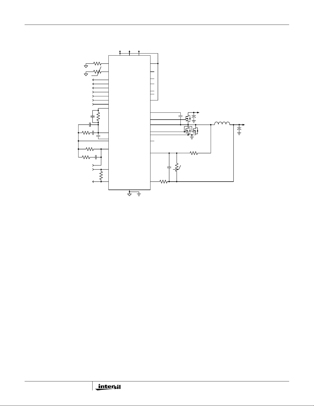
FIGURE 1. TYPICAL 3-PHASE APPLICATION CIRCUIT USING DCR SENSING
10
FN7557.1
March 18, 2010
ISL62883C
Simplified Application Circuits (Continued)
PGOOD
CLK_EN#
VID<0:6>
PSI#
DPRSLPVR
VR_ON
Rdroop
VCCSENSE
VSSSENSE
IMON
Rbias
Rntc
o
C
Rimon
Rfset
V+5 Vin
RBIAS
NTC
PGOOD
VR_TT#VR_TT#
CLK_EN#
VIDs
PSI#
DPRSLPVR
VR_ON
VW
ISL62883C
COMP
FB
VSEN
RTN
IMON
(Bottom Pad)
V+5
VCCP
VSS
VINVDD
PWM3
ISEN3
BOOT2
UGATE2
PHASE2
LGATE2
VSSP2
ISEN2
BOOT1
UGATE1
PHASE1
LGATE1
VSSP1
ISEN1
ISUM+
ISUM-
FCCM
ISL6208
PWM
Cs3
Cs2
Cs2
Cn
Ri
V+5
VCC
LGATE
GND
UGATE
PHASE
BOOT
Rs3
Rs2
Rs1
Rsum3
Rsum2
Rsum1
Vin
L3
L2
L1
Rsen3
Rsen2
Rsen1
V
o
FIGURE 2. TYPICAL 3-PHASE APPLICATION CIRCUIT USING RESISTOR SENSING
V+5 Vin
V+5
VCCP
VSS
VINVDD
PWM3
BOOT2
UGATE2
PHASE2
LGATE2
VSSP2
ISEN2
BOOT1
UGATE1
PHASE1
LGATE1a
VSSP1
ISEN1
ISUM+
ISUM-
Cn
Ri
Cs2
Cs1
Vin
L2
V
o
Rs2
L1
Rs1
Rsum2
Rn
o
C
Rsum1
PGOOD
CLK_EN#
VID<0:6>
PSI#
DPRSLPVR
VR_ON
Rdroop
VCCSENSE
VSSSENSE
IMON
Rbias
Rntc
o
C
Rimon
Rfset
RBIAS
NTC
PGOOD
VR_TT#VR_TT#
CLK_EN#
VIDs
PSI#
DPRSLPVR
VR_ON
VW
ISL62883C
COMP
FB2
FB
VSEN
RTN
IMON
(Bottom Pad)
FIGURE 3. TYPICAL 2-PGHASE APPLICATION CIRCUIT USING DCR SENSING
11
FN7557.1
March 18, 2010
ISL62883C
Simplified Application Circuits (Continued)
V+5 Vin
V+5
VCCP
VSS
VINVDD
PWM3
BOOT2
UGATE2
PHASE2
LGATE2
VSSP2
ISEN2
BOOT1
UGATE1
PHASE1
LGATE1a
VSSP1
ISEN1
ISUM+
ISUM-
Cn
Ri
PGOOD
CLK_EN#
VID<0:6>
PSI#
DPRSLPVR
VR_ON
Rdroop
VCCSENSE
VSSSENSE
IMON
Rbias
Rntc
o
C
Rimon
Rfset
RBIAS
NTC
PGOOD
VR_TT#VR_TT#
CLK_EN#
VIDs
PSI#
DPRSLPVR
VR_ON
VW
ISL62883C
COMP
FB2
FB
VSEN
RTN
IMON
(Bottom Pad)
Vin
L
Rsum
Rn
o
C
V
o
FIGURE 4. TYPICAL 1-PHASE APPLICATION CIRCUIT USING DCR SENSING
12
FN7557.1
March 18, 2010
ISL62883C
Theory of Operation
Multiphase R3™ Modulator
MASTER CLOCK CIRCUIT
VW
MASTER
CLOCK
gmVo
VW
Vcrs1
Crs1
VW
Vcrs2
Crs2
VW
Vcrs3
Crs3
FIGURE 5. R
VW
Vcrm
COMP
Master
Clock
Clock1
PWM1
Clock2
PWM2
Clock3
PWM3
FIGURE 6. R
COMP
Vcrm
Crm
Vcrs2 Vcrs1
3
™ MODULATOR OPERATION
PRINCIPLES IN STEADY STATE
MASTER
CLOCK
Phase
Sequencer
SLAVE CIRCUIT 1
Clock1
S
R
gm
SLAVE CIRCUIT 2
Clock2
Clock3
S
R
gm
SLAVE CIRCUIT 3
S
R
gm
3
™ MODULATOR CIRCUIT
Q
Q
Q
PWM1
PWM2
PWM3
Phase1
Phase2
Phase3
VW
Vcrs3
Clock1
Clock2
Clock3
L1
I
L1
L2
I
L2
L3
I
L3
Hysteretic
Window
Vo
Co
VW
COMP
Vcrm
Master
Clock
Clock1
PWM1
Clock2
PWM2
Clock3
PWM3
VW
Vcrs1
Vcrs3
Vcrs2
FIGURE 7. R
3
™ MODULATOROPERATION
PRINCIPLES IN LOAD INSERTION
RESPONSE
The ISL62883C is a multiphase regulators implementing
Intel™ IMVP-6.5™ protocol. It can be programmed for
1-, 2- or 3-phase operation. It uses Intersil patented
3
R
™ (Robust Ripple Regulator™) modulator. The R3™
modulator combines the best features of fixed
frequency PWM and hysteretic PWM while eliminating
many of their shortcomings. Figure 5 conceptually
shows the ISL62883C multiphase R
3
™ modulator
circuit, and Figure 6 shows the operation principles.
A current source flows from the VW pin to the COMP
pin, creating a voltage window set by the resistor
between the two pins. This voltage window is called
VW window in the following discussion.
Inside the IC, the modulator uses the master clock
circuit to generate the clocks for the slave circuits. The
modulator discharges the ripple capacitor C
current source equal to g
factor. C
voltage V
rm
crm
, where gm is a gain
mVo
is a sawtooth waveform
with a
rm
traversing between the VW and COMP voltages. It
resets to VW when it hits COMP, and generates a
one-shot master clock signal. A phase sequencer
distributes the master clock signal to the slave circuits.
If the ISL62883C is in 3-phase mode, the master clock
signal will be distributed to the three phases, and the
Clock1~3 signals will be 120° out-of-phase. If the
ISL62883C is in 2-phase mode, the master clock signal
will be distributed to Phases 1 and 2, and the Clock1
and Clock2 signals will be 180° out-of-phase. If the
13
FN7557.1
March 18, 2010
ISL62883C
ISL62883C is in 1-phase mode, the master clock signal
will be distributed to Phases 1 only and be the Clock1
signal.
Each slave circuit has its own ripple capacitor C
whose voltage mimics the inductor ripple current. A g
,
rs
m
amplifier converts the inductor voltage into a current
source to charge and discharge C
. The slave circuit
rs
turns on its PWM pulse upon receiving the clock signal,
and the current source charges C
V
hits VW, the slave circuit turns off the PWM pulse,
Crs
and the current source discharges C
Since the ISL62883C works with V
. When Crs voltage
rs
.
rs
, which are
crs
large-amplitude and noise-free synthesized signals,
the ISL62883C achieves lower phase jitter than
conventional hysteretic mode and fixed PWM mode
controllers. Unlike conventional hysteretic mode
converters, the ISL62883C has an error amplifier that
allows the controller to maintain a 0.5% output voltage
accuracy.
Figure 7 shows the operation principles during load
insertion response. The COMP voltage rises during load
insertion, generating the master clock signal more
quickly, so the PWM pulses turn on earlier, increasing
the effective switching frequency, which allows for
higher control loop bandwidth than conventional fixed
frequency PWM controllers. The VW voltage rises as
the COMP voltage rises, making the PWM pulses wider.
During load release response, the COMP voltage falls.
It takes the master clock circuit longer to generate the
next master clock signal so the PWM pulse is held off
until needed. The VW voltage falls as the VW voltage
falls, reducing the current PWM pulse width. This kind
of behavior gives the ISL62883C excellent response
speed.
The fact that all the phases share the same VW
window voltage also ensures excellent dynamic current
balance among phases.
ISL62883C can operate in diode emulation (DE) mode
to improve light load efficiency. In DE mode, the lowside MOSFET conducts when the current is flowing from
source to drain and doesn’t not allow reverse current,
emulating a diode. As Figure 8 shows, when LGATE is
on, the low-side MOSFET carries current, creating
negative voltage on the phase node due to the voltage
drop across the ON-resistance. The ISL62883C
monitors the current through monitoring the phase
node voltage. It turns off LGATE when the phase node
voltage reaches zero to prevent the inductor current
from reversing the direction and creating unnecessary
power loss.
If the load current is light enough, as Figure 8 shows,
the inductor current will reach and stay at zero before
the next phase node pulse, and the regulator is in
discontinuous conduction mode (DCM). If the load
current is heavy enough, the inductor current will
never reach 0A, and the regulator is in CCM although
the controller is in DE mode.
Figure 9 shows the operation principle in diode
emulation mode at light load. The load gets
incrementally lighter in the three cases from top to
bottom. The PWM on-time is determined by the VW
window size, therefore is the same, making the inductor
current triangle the same in the three cases. The
ISL62883C clamps the ripple capacitor voltage V
DE mode to make it mimic the inductor current. It takes
the COMP voltage longer to hit V
, naturally stretching
crs
the switching period. The inductor current triangles
move further apart from each other such that the
inductor current average value is equal to the load
current. The reduced switching frequency helps increase
light load efficiency.
CCM/DCM BOUNDARY
VW
Vcrs
crs
in
Diode Emulation and Period Stretching
Phase
UGATE
LGATE
IL
FIGURE 8. DIODE EMULATION
14
iL
LIGHT DCM
Vcrs
iL
Vcrs
iL
FIGURE 9. PERIOD STRETCHING
VW
VW
DEEP DCM
FN7557.1
March 18, 2010

ISL62883C
Start-up Timing
With the controller's VDD voltage above the POR
threshold, the start-up sequence begins when VR_ON
exceeds the 1.1V logic high threshold. Figure 10 shows
the typical start-up timing when the ISL62883C is
configured for CPU VR application. The ISL62883C uses
digital soft-start to ramp-up DAC to the boot voltage of
1.1V at about 2.5mV/µs. Once the output voltage is
within 10% of the boot voltage for 13 PWM cycles
(43µs for frequency = 300kHz), CLK_EN# is pulled low
and DAC slews at 5mV/µs to the voltage set by the VID
pins. PGOOD is asserted high in approximately 7ms.
Similar results occur if VR_ON is tied to V
soft-start sequence starting 120µs after VDD crosses the
POR threshold.
Figure 11 shows the typical start-up timing when the
ISL62883C is configured for GPU VR application. The
ISL62883C uses digital soft start to ramp up DAC to the
voltage set by the VID pins. The slew rate is 5mV/µs
when there is DPRSLPVR = 0, and is doubled when there
is DPRSLPVR = 1. Once the output voltage is within 10%
of the target voltage for 13 PWM cycles (43µs for
frequency = 300kHz), CLK_EN# is pulled low. PGOOD is
asserted high in approximately 7ms. Similar results occur
if VR_ON is tied to V
starting 120µs after V
VDD
VR_ON
DAC
CLK_EN#
PGOOD
FIGURE 10. SOFT-START WAVEFORMS FOR CPU VR
APPLICATION
VDD
VR_ON
DAC
CLK_EN#
PGOOD
FIGURE 11. SOFT-START WAVEFORMS FOR GPU VR
APPLICATION
, with the soft-start sequence
DD
crosses the POR threshold.
DD
5mV/µs
2.5mV/µs
800µs
SLEW
RATE
90%
120µs
13 SWITCHING
CYCLES
Vboot
90%
13 SWITCHING
CYCLES
VID COMMAND
VOLTAGE
~7ms
, with the
DD
VID
COMMAND
VOLTAGE
~7ms
Voltage Regulation and Load Line
Implementation
After the start sequence, the ISL62883C regulates the
output voltage to the value set by the VID inputs per
Table 1. The ISL62883C will control the no-load output
voltage to an accuracy of ±0.5% over the range of
0.75V to 1.5V. A differential amplifier allows voltage
sensing for precise voltage regulation at the
microprocessor die.
TABLE 1. VID TABLE
V
VID6 VID5 VID4 VID3 VID2 VID1 VID0
00000001.5000
00000011.4875
00000101.4750
00000111.4625
00001001.4500
00001011.4375
00001101.4250
00001111.4125
00010001.4000
00010011.3875
00010101.3750
00010111.3625
00011001.3500
00011011.3375
00011101.3250
00011111.3125
00100001.3000
00100011.2875
00100101.2750
00100111.2625
00101001.2500
00101011.2375
00101101.2250
00101111.2125
00110001.2000
00110011.1875
00110101.1750
00110111.1625
00111001.1500
00111011.1375
00111101.1250
00111111.1125
(V)
O
15
FN7557.1
March 18, 2010

ISL62883C
TABLE 1. VID TABLE (Continued)
V
VID6 VID5 VID4 VID3 VID2 VID1 VID0
01000001.1000
01000011.0875
01000101.0750
01000111.0625
01001001.0500
01001011.0375
01001101.0250
01001111.0125
01010001.0000
01010010.9875
01010100.9750
01010110.9625
01011000.9500
01011010.9375
01011100.9250
01011110.9125
01100000.9000
01100010.8875
01100100.8750
01100110.8625
01101000.8500
01101010.8375
01101100.8250
01101110.8125
01110000.8000
01110010.7875
01110100.7750
01110110.7625
01111000.7500
01111010.7375
01111100.7250
01111110.7125
10000000.7000
10000010.6875
10000100.6750
10000110.6625
10001000.6500
10001010.6375
10001100.6250
(V)
O
TABLE 1. VID TABLE (Continued)
V
VID6 VID5 VID4 VID3 VID2 VID1 VID0
10001110.6125
10010000.6000
10010010.5875
10010100.5750
10010110.5625
10011000.5500
10011010.5375
10011100.5250
10011110.5125
10100000.5000
10100010.4875
10100100.4750
10100110.4625
10101000.4500
10101010.4375
10101100.4250
10101110.4125
10110000.4000
10110010.3875
10110100.3750
10110110.3625
10111000.3500
10111010.3375
10111100.3250
10111110.3125
11000000.3000
11000010.2875
11000100.2750
11000110.2625
11001000.2500
11001010.2375
11001100.2250
11001110.2125
11010000.2000
11010010.1875
11010100.1750
11010110.1625
11011000.1500
11011010.1375
(V)
O
16
FN7557.1
March 18, 2010

ISL62883C
TABLE 1. VID TABLE (Continued)
V
VO
(V)
O
VID6 VID5 VID4 VID3 VID2 VID1 VID0
11011100.1250
11011110.1125
11100000.1000
11100010.0875
11100100.0750
11100110.0625
11101000.0500
11101010.0375
11101100.0250
11101110.0125
11110000.0000
11110010.0000
11110100.0000
11110110.0000
11111000.0000
11111010.0000
11111100.0000
11111110.0000
Rdroop
COMP
FB
E/A
INTERNAL
Σ
Idroop
VDAC
Vdroop
DAC
X 1
VIDs
RTN
VSS
TO IC
FIGURE 12. DIFFERENTIAL SENSING AND LOAD LINE
IMPLEMENTATION
VCC
“CATCH”
RESISTOR
VID<0:6>
VSS
“CATCH”
RESISTOR
SENSE
VR LOCAL
SENSE
As the load current increases from zero, the output
voltage will droop from the VID table value by an amount
proportional to the load current to achieve the load line.
The ISL62883C can sense the inductor current through
the intrinsic DC Resistance (DCR) of the inductors as
shown in Figure 1 on page 10 or through resistors in
series with the inductors as shown in Figure 2 on
page 11. In both methods, capacitor C
voltage
n
represents the inductor total currents. A droop amplifier
converts C
the gain set by resistor R
voltage into an internal current source with
n
. The current source is used for
i
load line implementation, current monitor and
overcurrent protection.
Figure 12 shows the load line implementation. The
ISL62883C drives a current source I
out of the FB
droop
pin, described by Equation 1.
I
droop
=
Cn
------------------
R
i
(EQ. 1)
2xV
When using inductor DCR current sensing, a single NTC
element is used to compensate the positive temperature
coefficient of the copper winding thus sustaining the load
line accuracy with reduced cost.
flows through resistor R
I
droop
and creates a
droop
voltage drop as shown in Equation 2.
V
droopRdroopIdroop
V
is the droop voltage required to implement load
droop
line. Changing R
the load line slope. Since I
protection level, it is recommended to first scale I
×=
droop
or scaling I
also sets the overcurrent
droop
can both change
droop
(EQ. 2)
droop
based on OCP requirement, then select an appropriate
value to obtain the desired load line slope.
R
droop
Differential Sensing
Figure 12 also shows the differential voltage sensing
scheme. VCC
voltage sensing signals from the processor die. A unity
gain differential amplifier senses the VSS
and add it to the DAC output. The error amplifier
regulates the inverting and the non-inverting input
voltages to be equal as shown in Equation 3:
VCC
SENSE
V+
Rewriting Equation 3 and substitution of Equation 2 gives
VCC
SENSE
VSS
– V
Equation 4 is the exact equation required for load line
implementation.
The VCC
SENSE
processor die. The feedback will be open circuit in the
absence of the processor. As Figure 12 shows, it is
recommended to add a “catch” resistor to feed the VR
local output voltage back to the compensator, and add
another “catch” resistor to connect the VR local output
ground to the RTN pin. These resistors, typically
10Ω~100Ω, will provide voltage feedback if the system is
powered up without a processor installed.
and VSS
SENSE
droop
SENSE
and VSS
SENSE
V
VSS
+=
DAC
SENSE
SENSE
DACRdroopIdroop
signals come from the
are the remote
voltage
SENSE
×–=
(EQ. 3)
(EQ. 4)
17
FN7557.1
March 18, 2010

ISL62883C
Phase Current Balancing
Rdcr3
L3
Phase3
ISEN3
INTERNAL
TO IC
ISEN2
ISEN1
FIGURE 13. CURRENT BALANCING CIRCUIT
Rs
Cs
Phase2
Rs
Cs
Phase1
Rs
Cs
IL3
L2
IL2
L1
IL1
The ISL62883C monitors individual phase average
current by monitoring the ISEN1, ISEN2, and ISEN3
voltages. Figure 13 shows the current balancing circuit
recommended for ISL62883C. Each phase node
voltage is averaged by a low-pass filter consisting of R
and C
, and presented to the corresponding ISEN pin.
s
R
should be routed to inductor phase-node pad in
s
order to eliminate the effect of phase node parasitic
PCB DCR. Equations 5 thru 7 give the ISEN pin
voltages:
V
ISEN1
V
ISEN2
V
ISEN3
where R
R
pcb2
dcr1
and R
R
+()IL1×=
dcr1Rpcb1
R
+()IL2×=
dcr2Rpcb2
R
+()IL3×=
dcr3Rpcb3
, R
pcb3
dcr2
and R
are inductor DCR; R
dcr3
are parasitic PCB DCR between the
inductor output side pad and the output voltage rail;
and I
, IL2 and IL3 are inductor average currents.
L1
The ISL62883C will adjust the phase pulse-width
relative to the other phases to make
V
ISEN1=VISEN2=VISEN3
I
L1=IL2=IL3
and R
pcb1=Rpcb2
, when there are R
=R
, thus to achieve
.
pcb3
Using same components for L1, L2 and L3 will provide
a good match of R
will determine R
dcr1
pcb1
, R
, R
pcb2
dcr2
and R
and R
recommended to have symmetrical layout for the
power delivery path between each inductor and the
output voltage rail, such that R
pcb1
Rpcb3
Rdcr2
Rpcb2
Rdcr1
Rpcb1
=R
dcr1
. Board layout
dcr3
. It is
pcb3
=R
pcb2=Rpcb3
V
o
(EQ. 5)
(EQ. 6)
(EQ. 7)
pcb1
dcr2=Rdcr3
.
Rdcr3
pcb1
, R
L3
L2
L1
IL3
Rdcr2
IL2
Rdcr1
IL1
pcb2
Phase3
ISEN3
Cs
INTERNAL
TO IC
ISEN2
ISEN1
FIGURE 14. DIFFERENTIAL-SENSING CURRENT
Sometimes, it is difficult to implement symmetrical
s
layout. For the circuit shown in Figure 13, asymmetric
Phase2
Cs
Phase1
Cs
BALANCING CIRCUIT
V3p
Rs
Rs
Rs
V2p
Rs
Rs
Rs
V1p
Rs
Rs
Rs
layout causes different R
Rpcb3
V3n
Rpcb2
V2n
Rpcb1
V1n
and R
current imbalance. Figure 14 shows a
differential-sensing current balancing circuit
recommended for ISL62883C. The current sensing
traces should be routed to the inductor pads so they
only pick up the inductor DCR voltage. Each ISEN pin
sees the average voltage of three sources: its own
phase inductor phase-node pad, and the other two
phases inductor output side pads. Equations 8 thru 10
give the ISEN pin voltages:
V
ISEN1V1pV2nV3n
,
V
ISEN2V1nV2pV3n
V
ISEN3V1nV2nV3p
The ISL62883C will make V
++=
++=
++=
= V
ISEN1
ISEN2
as shown in Equations 11 and 12:
++ V
V
1pV2nV3n
++ V
V
1nV2pV3n
++=
1nV2pV3n
++=
1nV2nV3p
Rewriting Equation 11 gives Equation 13:
V
– V
1pV1n
–=
2pV2n
and rewriting Equation 12 gives Equation 14:
V
– V
2pV2n
–=
3pV3n
Combining Equations 13 and 14 gives:
– V
V
1pV1n
– V
2pV2n
–==
3pV3n
pcb3
= V
V
o
thus
(EQ. 8)
(EQ. 9)
(EQ. 10)
ISEN3
(EQ. 11)
(EQ. 12)
(EQ. 13)
(EQ. 14)
(EQ. 15)
18
Therefore:
R
× R
dcr1IL1
× R
dcr2IL2
×==
dcr3IL3
(EQ. 16)
FN7557.1
March 18, 2010

ISL62883C
Current balancing (IL1=IL2=IL3) will be achieved
when there is R
R
will not have any effect.
pcb3
Since the slave ripple capacitor voltages mimic the
inductor currents, R
excellent current balancing during steady state and
dynamic operations. Figure 15 shows current balancing
performance of the ISL62883C evaluation board with load
transient of 12A/51A at different rep rates. The inductor
currents follow the load current dynamic change with the
output capacitors supplying the difference. The inductor
currents can track the load current well at low rep rate,
but cannot keep up when the rep rate gets into the
hundred-kHz range, where it’s out of the control loop
bandwidth. The controller achieves excellent current
balancing in all cases installed.
CCM Switcing Frequency
=R
dcr1
dcr2=Rdcr3
3
™ modulator can naturally achieve
. R
pcb1
, R
pcb2
and
REP RATE = 10kHz
REP RATE = 25kHz
The R
resistor between the COMP and the VW pins
fset
sets the sets the VW windows size, therefore sets the
switching frequency. When the ISL62883C is in
continuous conduction mode (CCM), the switching
frequency is not absolutely constant due to the nature of
3
™ modulator. As explained in the Multiphase R3™
the R
Modulator section, the effective switching frequency will
increase during load insertion and will decrease during
load release to achieve fast response. On the other hand,
the switching frequency is relatively constant at steady
state. Variation is expected when the power stage
condition, such as input voltage, output voltage, load,
etc. changes. The variation is usually less than 15% and
doesn’t have any significant effect on output voltage
ripple magnitude. Equation 17 gives an estimate of the
frequency-setting resistor R
value. 8kΩ R
fset
fset
gives
approximately 300kHz switching frequency. Lower
resistance gives higher switching frequency.
R
kΩ() Period μs()0.29–()2.65×=
fset
(EQ. 17)
REP RATE = 50kHz
REP RATE = 100kHz
19
REP RATE = 200kHz
FIGURE 15. ISL62883 EVALUATION BOARD CURRENT
BALANCING DURING DYNAMIC
OPERATION. CH1: IL1, CH2: I
IL2, CH4: IL3
LOAD
, CH3:
FN7557.1
March 18, 2010

ISL62883C
Modes of Operation
TABLE 2. ISL62883C CONFIGURATIONS
OVERSHOOT
R
BIAS
PWM3 ISEN2 CLK_EN#
To
External
Driver
Tied to
5V
3-phase CPU
Config.
3-phase GPU
Config.
2-phase CPU
Config.
2-phase GPU
Config.
1-phase CPU
Config.
1-phase GPU
Config.
To
Power
Stage
Tied to 5Vx 147 1-phase
TABLE 3. ISL62883C MODES OF OPERATION
CONFIG. PSI# DPRSLPVR
External
pull-up
Tied to
GND or
floating
External
pull-up
Tied to
GND or
floating
0 0 2-phase CCM 5mV/µs
1 0 3-phase CCM
011-phase DE
111-phase DE
0 0 2-phase CCM
1 0 3-phase CCM
0 1 1-phase DE 10mV/µs
111-phase DE
0 0 1-phase CCM 5mV/µs
1 0 2-phase CCM
011-phase DE
111-phase DE
0 0 1-phase CCM
1 0 2-phase CCM
0 1 1-phase DE 10mV/µs
111-phase DE
x 0 1-phase CCM 5mV/µs
x 0 1-phase CCM
(kΩ) CONFIG.
147 3-phase
CPU VR
47 Enabled
147 3-phase
GPU VR
47 Enabled
147 2-phase
CPU VR
47 Enabled
147 2-phase
GPU VR
47 Enabled
CPU
47 1-phase
GPU
OPERATIONAL
MODE
11-phase DE
1 1-phase DE 10mV/µs
The ISL62883C can be configured for 3, 2 or 1-phase
operation.
For 2-phase configuration, tie the PWM3 pin to 5V. In this
configuration, phases 1 and 2 are active. For 1-phase
configuration, tie the ISEN2 pin to 5V. In this
configuration, only phase-1 is active.
REDUCTION
FUNCTION
Disabled
Disabled
Disabled
Disabled
See Table 4
SLEW
RATE
Table 2 shows the ISL62883C configurations,
programmed by the PWM3 pin, the ISEN2 pin, the
CLK_EN# pin status and the R
BIAS
value.
When the ISL62883C is in 3- or 2-phase configuration,
external pull-up on the CLK_EN# pin puts the ISL62883C
in CPU VR configuration; Tying the CLK_EN# pin to GND
or leaving it floating puts the ISL62883C in GPU VR
configuration. In 3- or 2-phase configuration,
=147kΩ disables the overshoot reduction function
R
BIAS
and R
=47kΩ enables it.
BIAS
If the PWM3 pin and the ISEN2 pin are both tied to 5V,
the ISL62883C is in 1-phase configuration. The CLK_EN#
pin status has no effect. R
ISL62883C in CPU VR configuration and R
= 147kΩ puts the
BIAS
BIAS
= 47kΩ
puts the ISL62883C in GPU configuration. In 1-phase
configuration, the enabling and disabling of the
overshoot reduction function are programmed by the
resistance from COMP to GND, as Table 4 shows.
Table 3 shows the ISL62883C operational modes,
programmed by the logic status of the PSI# and the
DPRSLPVR pins.
In 3-phase configuration, the ISL62883C enters 2-phase
CCM for (PSI# = 0 and DPRSLPVR = 0). It drops phase 3
and operates phases 1 and 2 180° out-of-phase. It also
reduces the overcurrent and the way-overcurrent
protection levels to 2/3 of the initial values. The
ISL62883C enters 1-phase DE mode for DPRSLPVR = 1
by dropping phase 2 and reduces the overcurrent and
the way-overcurrent protection levels to 1/3 of the initial
values.
In 2-phase configuration, the ISL62883C enters 1-phase
CCM for (PSI# = 0 and DPRSLPVR = 0). It drops phase 2
and reduces the overcurrent and the way-overcurrent
protection levels to 1/2 of the initial values. The
ISL62883C enters 1-phase DE mode for DPRSLPVR = 1
by dropping phase 2 and reduces the overcurrent and
the way-overcurrent protection levels to 1/3 of the initial
values.
In 1-phase configuration, the ISL62883C does not
change the operational mode when the PSI# signal
changes status. It enters 1-phase DE mode when
DLPRSLPVR = 1.
Dynamic Operation
When the ISL62883C is configured for CPU VR
application, it responds to VID changes by slewing to the
new voltage at 5mV/µs slew rate. As the output
approaches the VID command voltage, the dv/dt
moderates to prevent overshoot. Geyserville-III
transitions commands one LSB VID step (12.5mV) every
2.5µs, controlling the effective dv/dt at 5mv/µs. The
ISL62883C is capable of 5mV/µs slew rate.
When the ISL62883C is configured for GPU VR
application, it responds to VID changes by slewing to the
new voltage at a slew rate set by the logic status on the
DPRSLPVR pin. The slew rate is 5mV/µs when
DPRSLPVR=0 and is doubled when DPRSLPVR = 1.
20
FN7557.1
March 18, 2010

ISL62883C
When the ISL62883C is in DE mode, it will actively drive
the output voltage up when the VID changes to a higher
value. The DE mode operation will resume after reaching
the new voltage level. If the load is light enough to
warrant DCM, it will enter DCM after the inductor current
has crossed zero for four consecutive cycles. The
ISL62883C will remain in DE mode when the VID
changes to a lower value. The output voltage will decay
to the new value and the load will determine the slew
rate. Overvoltage protection is blanked during VID down
transition in DE mode until the output voltage is within
60mV of the VID value.
During load insertion response, the Fast Clock function
increases the PWM pulse response speed. The
ISL62883C monitors the VSEN pin voltage and compares
it to 100ns-filtered version. When the unfiltered version
is 20mV below the filtered version, the controller knows
there is a fast voltage dip due to load insertion, hence
issues an additional master clock signal to deliver a PWM
pulse immediately.
3™
The R
modulator intrinsically has voltage
feed-forward. The output voltage is insensitive to a fast
slew rate input voltage change.
Protections
The ISL62883C provides overcurrent, current-balance,
undervoltage, overvoltage, and over-temperature
protections.
The ISL62883C determines overcurrent protection
(OCP) by comparing the average value of the droop
current I
It declares OCP when I
120µs. A resistor R
programs the OCP current source threshold, as well as
the overshoot reduction function in 1-phase
configuration, as Table 4 shows. It is recommended to
use the nominal R
the R
comp
the internal OCP threshold accordingly. It remembers
the R
comp
POR threshold.
TABLE 4. ISL62883C R
R
comp
MIN
NOM
(kΩ)
(kΩ)
none none 60 40 60 Disabled
320 400 480 68 45.3 68
210 235 260 62 41.3 62
155 165 175 54 36 54
104 120 136 56 37.33 60 Enabled
78 85 92 58 38.7 68
62 66 70 64 42.7 62
45 50 55 66 44 54
with an internal current source threshold.
droop
comp
comp
is above the threshold for
droop
from the COMP pin to GND
value. The ISL62883C detects
value at the beginning of start-up, and sets
value until the VR_ON signal drops below the
PROGRAMMABILITY
comp
3-PHASE
CONFIG.
MAX
(kΩ)
2-PHASE
CONFIG. 1-PHASECONFIG.
OCP THRESHOLD
(µA)
OVERSHOOT
REDUCTION
FUNCTION
The default OCP threshold is the value when R
comp
is not
populated. It is recommended to scale the droop current
I
such that the default OCP threshold gives
droop
approximately the desired OCP level, then use R
comp
to
fine tune the OCP level if necessary.
For overcurrent conditions above 2.5x the OCP level, the
PWM outputs will immediately shut off and PGOOD will
go low to maximize protection. This protection is also
referred to as way-overcurrent protection or
fast-overcurrent protection, for short-circuit protections.
The ISL62883C monitors the ISEN pin voltages to
determine current-balance protection. If the ISEN pin
voltage difference is greater than 9mV for 1ms, the
controller will declare a fault and latch off.
The ISL62883C will declare undervoltage (UV) fault and
latch off if the output voltage is less than the VID set
value by 300mV or more for 1ms. It’ll turn off the PWM
outputs and de-assert PGOOD.
The ISL62883C has two levels of overvoltage
protections. The first level of overvoltage protection is
referred to as PGOOD overvoltage protection. If the
output voltage exceeds the VID set value by +200mV for
1ms, the ISL62883C will declare a fault and de-assert
PGOOD.
The ISL62883C takes the same actions for all of the
above fault protections: de-assertion of PGOOD and
turn-off of the high-side and low-side power MOSFETs.
Any residual inductor current will decay through the
MOSFET body diodes. These fault conditions can be reset
by bringing VR_ON low or by bringing V
below the
DD
POR threshold. When VR_ON and VDD return to their
high operating levels, a soft-start will occur.
The second level of overvoltage protection is different.
If the output voltage exceeds 1.55V, the ISL62883C will
immediately declare an OV fault, de-assert PGOOD, and
turn on the low-side power MOSFETs. The low-side
power MOSFETs remain on until the output voltage is
pulled down below 0.85V when all power MOSFETs are
turned off. If the output voltage rises above 1.55V
again, the protection process is repeated. This behavior
provides the maximum amount of protection against
shorted high-side power MOSFETs while preventing
output ringing below ground. Resetting VR_ON cannot
clear the 1.55V OVP. Only resetting V
will clear it. The
DD
1.55V OVP is active all the time when the controller is
enabled, even if one of the other faults have been
declared. This ensures that the processor is protected
against high-side power MOSFET leakage while the
MOSFETs are commanded off.
The ISL62883C has a thermal throttling feature. If the
voltage on the NTC pin goes below the 1.18V OT
threshold, the VR_TT# pin is pulled low indicating the
need for thermal throttling to the system. No other
action is taken within the ISL62883C in response to NTC
pin voltage.
Table 5 summarizes the fault protections.
21
FN7557.1
March 18, 2010

ISL62883C
TABLE 5. FAULT PROTECTION SUMMARY
FAULT
DURATION
BEFORE
FAULT TYPE
Overcurrent 120µs PWM tri-state,
Way-Overcurrent
(2.5xOC)
Overvoltage
+200mV
Undervoltage 300mV
Phase Current
Unbalance
Overvoltage 1.55V Immediately Low-side
Over-Temperature 1ms N/A
PROTECTION
<2µs
1ms
PROTECTION
ACTION
PGOOD
latched low
MOSFET on
until
<0.85V, then
PWM tri-state,
PGOOD
latched low.
Vcore
FAULT
RESET
VR_ON
toggle or
VDD
toggle
VDD
toggle
Current Monitor
The ISL62883C provides the current monitor function.
The IMON pin outputs a high-speed analog current
source that is 3 times of the droop current flowing out of
the FB pin. Thus Equation 18:
I
IMON
As Figures 1 and 2 show, a resistor R
3I
×=
droop
is connected to
imon
(EQ. 18)
the IMON pin to convert the IMON pin current to voltage.
A capacitor can be paralleled with R
to filter the
imon
voltage information. The IMVP-6.5™ specification
requires that the IMON voltage information be referenced
SENSE
.
to VSS
The IMON pin voltage range is 0V to 1.1V. A clamp circuit
prevents the IMON pin voltage from going above 1.1V.
FB2 Function
The FB2 function is only available when the ISL62883C is
in 2-phase configuration.
CONTROLLER IN
2-PHASE MODE
C2
R3
VSEN
R1
Figure 16 shows the FB2 function. A switch (called FB2
switch) turns on to short the FB and the FB2 pins when
the controller is in 2-phase mode. Capacitors C3.1 and
C3.2 are in parallel, serving as part of the compensator.
When the controller enters 1-phase mode, the FB2
switch turns off, removing C3.2 and leaving only C3.1 in
C1
R2
C3.1
C3.2
FB2
E/A
FB
VREF
FIGURE 16. FB2 FUNCTION
CONTROLLER IN
VSEN
COMP
1-PHASE MODE
C2
R1
R3
FB2
FB
VREF
C1
R2
C3.1
C3.2
E/A
COMP
the compensator. The compensator gain will increase
with the removal of C3.2. By properly sizing C3.1 and
C3.2, the compensator cab be optimal for both 2-phase
mode and 1-phase mode.
When the FB2 switch is off, C3.2 is disconnected from the
FB pin. However, the controller still actively drives the
FB2 pin voltage to follow the FB pin voltage such that
C3.2 voltage always follows C3.1 voltage. When the
controller turns on the FB2 switch, C3.2 will be
reconnected to the compensator smoothly.
The FB2 function ensures excellent transient response in
both 2-phase mode and 1-phase mode. If one decides
not to use the FB2 function, simply populate C3.1 only.
Adaptive Body Diode Conduction Time
Reduction
In DCM, the controller turns off the low-side MOSFET
when the inductor current approaches zero. During ontime of the low-side MOSFET, phase voltage is negative
and the amount is the MOSFET r
DS(ON)
voltage drop,
which is proportional to the inductor current. A phase
comparator inside the controller monitors the phase
voltage during on-time of the low-side MOSFET and
compares it with a threshold to determine the
zero-crossing point of the inductor current. If the
inductor current has not reached zero when the low-side
MOSFET turns off, it’ll flow through the low-side MOSFET
body diode, causing the phase node to have a larger
voltage drop until it decays to zero. If the inductor
current has crossed zero and reversed the direction when
the low-side MOSFET turns off, it’ll flow through the highside MOSFET body diode, causing the phase node to
have a spike until it decays to zero. The controller
continues monitoring the phase voltage after turning off
the low-side MOSFET and adjusts the phase comparator
threshold voltage accordingly in iterative steps such that
the low-side MOSFET body diode conducts for
approximately 40ns to minimize the body diode-related
loss.
Overshoot Reduction Function
The ISL62883C has an optional overshoot reduction
function. Tables 2 and 4 show how to enable and disable
it.
When a load release occurs, the energy stored in the
inductors will dump to the output capacitor, causing
output voltage overshoot. The inductor current
freewheels through the low-side MOSFET during this
period of time. The overshoot reduction function turns off
the low-side MOSFET during the output voltage
overshoot, forcing the inductor current to freewheel
through the low-side MOSFET body diode. Since the body
diode voltage drop is much higher than MOSFET r
voltage drop, more energy is dissipated on the low-side
MOSFET therefore the output voltage overshoot is lower.
If the overshoot reduction function is enabled, the
ISL62883C monitors the COMP pin voltage to determine
the output voltage overshoot condition. The COMP
voltage will fall and hit the clamp voltage when the
DS(ON)
22
FN7557.1
March 18, 2010

ISL62883C
output voltage overshoots. The ISL62883C will turn off
LGATE1 and LGATE2 when COMP is being clamped. All
the low-side MOSFETs in the power stage will be turned
off. When the output voltage has reached its peak and
starts to come down, the COMP voltage starts to rise and
is no longer clamped. The ISL62883C will resume normal
PWM operation.
When PSI# is low, indicating a low power state of the
CPU, the controller will disable the overshoot reduction
function as large magnitude transient event is not
expected and overshoot is not a concern.
While the overshoot reduction function reduces the
output voltage overshoot, energy is dissipated on the
low-side MOSFET, causing additional power loss. The
more frequent transient event, the more power loss
dissipated on the low-side MOSFET. The MOSFET may
face severe thermal stress when transient events
happen at a high repetitive rate. User discretion is
advised when this function is enabled.
Key Component Selection
R
BIAS
The ISL62883C uses a resistor (1% or better tolerance
is recommended) from the RBIAS pin to GND to
establish highly accurate reference current sources
inside the IC. Refer to Table 2 to select the resistance
according to desired configuration. Do not connect any
other components to this pin. Do not connect any
capacitor to the RBIAS pin as it will create instability.
Care should be taken in layout that the resistor is placed
very close to the RBIAS pin and that a good quality signal
ground is connected to the opposite side of the R
resistor.
Inductor DCR Current-Sensing Network
Phase2 Phase3
Phase1
Rsum
Rsum
Rsum
L
DCRLDCR
DCR
Io
FIGURE 17. DCR CURRENT-SENSING NETWORK
L
Rntcs
Rntc
Ro
Ro
Ro
Rp
Cn
Vcn
Ri
BIAS
ISUM+
ISUM-
Figure 17 shows shows the inductor DCR currentsensing network for a 3-phase solution. An inductor
current flows through the DCR and creates a voltage
drop. Each inductor has two resistors in R
sum
and Ro
connected to the pads to accurately sense the inductor
current by sensing the DCR voltage drop. The R
R
resistors are connected in a summing network as
o
sum
and
shown, and feed the total current information to the
NTC network (consisting of R
capacitor C
. R
is a negative temperature coefficient
n
ntc
ntcs
, R
and Rp) and
ntc
(NTC) thermistor, used to temperature-compensate the
inductor DCR change.
The inductor output side pads are electrically shorted in
the schematic, but have some parasitic impedance in
actual board layout, which is why one cannot simply
short them together for the current-sensing summing
network. It is recommended to use 1W~10W R
create quality signals. Since R
value is much smaller
o
o
to
than the rest of the current sensing circuit, the following
analysis will ignore it for simplicity.
The summed inductor current information is presented
to the capacitor C
. Equations 19 thru 23 describe the
n
frequency-domain relationship between inductor total
current I
V
Cn
R
ntcnet
A
cs
ω
L
ω
sns
(s) and Cn voltage VCn(s):
o
⎛⎞
R
⎜⎟
ntcnet
------------------------------------------
s()
⎜⎟
⎜⎟
R
⎝⎠
----------------------------------------------------
=
1
-----------------------
s()
=
1
DCR
-------------
=
L
--------------------------------------------------------
=
R
ntcnet
------------------------------------------
R
ntcnet
+
ntcnet
R
+()Rp×
ntcsRntc
R
++
ntcsRntcRp
s
------ -
+
ω
L
s
------------ -
+
ω
sns
1
R
sum
-------------- -
×
N
R
sum
-------------- -
+
N
R
sum
-------------- -
N
DCR
-------------
×
N
×
C
n
s()× Acs× s()=
I
o
(EQ. 19)
(EQ. 20)
(EQ. 21)
(EQ. 22)
(EQ. 23)
where N is the number of phases.
Transfer function A
(s) always has unity gain at DC.
cs
The inductor DCR value increases as the winding
temperature increases, giving higher reading of the
inductor DC current. The NTC R
its temperature decreases. Proper selections of R
R
, Rp and R
ntcs
parameters ensure that VCn
ntc
values decreases as
ntc
sum
,
represent the inductor total DC current over the
temperature range of interest.
23
FN7557.1
March 18, 2010

ISL62883C
There are many sets of parameters that can properly
temperature-compensate the DCR change. Since the
NTC network and the R
divider, V
is always a fraction of the inductor DCR
cn
voltage. It is recommended to have a higher ratio of V
resistors form a voltage
sum
cn
to the inductor DCR voltage, so the droop circuit has
higher signal level to work with.
A typical set of parameters that provide good
temperature compensation are: R
R
= 11kΩ, R
p
= 2.61kΩ and R
ntcs
sum
ntc
= 10kΩ
= 3.65kΩ,
(ERT-J1VR103J). The NTC network parameters may
need to be fine tuned on actual boards. One can apply
full load DC current and record the output voltage
reading immediately; then record the output voltage
reading again when the board has reached the thermal
steady state. A good NTC network can limit the output
voltage drift to within 2mV. It is recommended to follow
the Intersil evaluation board layout and current-sensing
network parameters to minimize engineering time.
V
(s) also needs to represent real-time Io(s) for the
Cn
controller to achieve good transient response. Transfer
function A
needs to match w
all frequencies. By forcing w
(s) has a pole w
cs
and w
L
and a zero wL. One
sns
so Acs(s) is unity gain at
sns
equal to w
L
and solving
sns
for the solution, Equation 24 gives Cn value.
-------------------------------------------------------------- -
C
=
n
R
ntcnet
------------------------------------------
R
ntcnet
For example, given N = 3, R
R
= 2.61kΩ, R
ntcs
R
-------------- -
×
R
-------------- -
+
L
sum
N
DCR×
sum
N
= 3.65kΩ, Rp = 11kΩ,
= 10kΩ, DCR = 0.88mΩ and
ntc
sum
(EQ. 24)
L = 0.36µH, Equation 24 gives Cn= 0.406µF.
i
o
V
o
FIGURE 18. DESIRED LOAD TRANSIENT RESPONSE
FIGURE 19. LOAD TRANSIENT RESPONSE WHEN Cn
FIGURE 20. LOAD TRANSIENT RESPONSE WHEN Cn
WAVEFORMS
IS TOO SMALL
IS TOO LARGE
i
o
V
o
i
o
V
o
Assuming the compensator design is correct, Figure 18
shows the expected load transient response waveforms
if C
is correctly selected. When the load current I
n
has a square change, the output voltage V
also has
core
core
a square response.
value is too large or too small, VCn(s) will not
If C
n
accurately represent real-time I
(s) and will worsen the
o
transient response. Figure 19 shows the load transient
response when Cn is too small. V
will sag excessively
core
upon load insertion and may create a system failure.
Figure 20 shows the transient response when C
large. V
is sluggish in drooping to its final value.
core
is too
n
There will be excessive overshoot if load insertion occurs
during this time, which may potentially hurt the CPU
reliability.
24
i
o
i
L
V
o
RING
BACK
FIGURE 21. OUTPUT VOLTAGE RING BACK PROBLEM
FN7557.1
March 18, 2010

ISL62883C
ISUM+
Rntcs
Rp
Rntc
FIGURE 22. OPTIONAL CIRCUITS FOR RING BACK
REDUCTION
Cn.1
Rn
OPTIONAL
Vcn
Cn.2
Ri
Cip
Rip
OPTIONAL
ISUM-
Figure 21 shows the output voltage ring back problem
during load transient response. The load current io has a
fast step change, but the inductor current i
cannot
L
accurately follow. Instead, iL responds in first order
system fashion due to the nature of current loop. The
ESR and ESL effect of the output capacitors makes the
output voltage V
dip quickly upon load current change.
o
However, the controller regulates Vo according to the
droop current i
, which is a real-time representation
droop
of iL; therefore it pulls Vo back to the level dictated by iL,
causing the ring back problem. This phenomenon is not
observed when the output capacitor have very low ESR
and ESL, such as all ceramic capacitors.
Figure 22 shows two optional circuits for reduction of the
ring back.
is the capacitor used to match the inductor time
C
n
constant. It usually takes the parallel of two (or more)
capacitors to get the desired value. Figure 22 shows that
two capacitors C
n.1
and C
an optional component to reduce the V
steady state, C
n.1
+ C
capacitance. At the beginning of i
capacitance is less because R
of the C
when C
branch. As Figure 19 explains, Vo tends to dip
n.1
is too small, and this effect will reduce the Vo
n
ring back. This effect is more pronounced when C
much larger than C
n.2
are in parallel. Resistor Rn is
n.2
provides the desired Cn
n.2
increases the impedance
n
ring back. At
o
change, the effective
o
is
n.1
. It is also more pronounced when
Rn is bigger. However, the presence of Rn increases the
ripple of the V
signal if C
n
recommended to keep C
value usually is a few ohms. C
is too small. It is
n.2
greater than 2200pF. Rn
n.2
n.1
, C
and Rn values
n.2
should be determined through tuning the load transient
response waveforms on an actual board.
and Cip form an R-C branch in parallel with Ri,
R
ip
providing a lower impedance path than R
beginning of i
change. Rip and Cip do not have any
o
at the
i
effect at steady state. Through proper selection of Rip
and C
V
values, i
ip
will not ring back. The recommended value for Rip is
o
can resemble io rather than iL, and
droop
100Ω. Cip should be determined through tuning the load
transient response waveforms on an actual board. The
recommended range for C
is 100pF~2000pF. However,
ip
it should be noted that the Rip -Cip branch may distort
the i
real inductor current, i
which may adversely affect i
waveform. Instead of being triangular as the
droop
may have sharp spikes,
droop
average value
droop
detection and therefore may affect OCP accuracy. User
discretion is advised.
Resistor Current-Sensing Network
Phase1
L
DCR
Rsen
FIGURE 23. RESISTOR CURRENT-SENSING NETWORK
Figure 23 shows the resistor current-sensing network for
a 2-phase solution. Each inductor has a series
current-sensing resistor R
connected to the R
inductor current information. The R
are connected to capacitor Cn. R
filter for noise attenuation. Equations 25 thru 27 give
(s) expression
V
Cn
VCns()
A
Rsen
ω
Rsen
Transfer function A
Current-sensing resistor R
significant variation over-temperature, so there is no
need for the NTC network.
The recommended values are R
= 5600pF.
C
n
Phase2 Phase3
DCRLDCR
Rsen Rsen
Io
R
sen
-------------
N
---------------------- -
s()
=
+
1
1
-----------------------------
=
R
sum
-------------- -
N
I
1
------------ -
ω
sns
×
C
L
Rsum
Rsum
Rsum
Ro
Ro
Ro
. R
sen
pads to accurately capture the
sen
s()× A
× s()=
o
Rsen
s
n
(s) always has unity gain at DC.
Rsen
value will not have
sen
Vcn
and Ro are
sum
and Ro resistors
sum
and Cn form a a
sum
= 1kΩ and
sum
Cn
Ri
ISUM+
ISUM-
(EQ. 25)
(EQ. 26)
(EQ. 27)
Overcurrent Protection
Refer to Equation 1 on page 17 and Figures 17, 21 and
23; resistor R
page 21 shows the internal OCP threshold. It is
recommended to design I
resistor.
sets the droop current I
i
without using the R
droop
. Table 4 on
droop
comp
25
FN7557.1
March 18, 2010

ISL62883C
For example, the OCP threshold is 60µA for 3-phase
solution. We will design I
to be 40.9µA at full load,
droop
so the OCP trip level is 1.5x of the full load current.
For inductor DCR sensing, Equation 28 gives the DC
relationship of V
⎛⎞
⎜⎟
V
------------------------------------------
⎜⎟
Cn
⎜⎟
R
⎝⎠
ntcnet
R
ntcnet
cn
+
(s) and Io(s).
DCR
-------------
×
R
-------------- -
sum
N
N
×=
I
o
(EQ. 28)
Substitution of Equation 28 into Equation 1 gives
Equation 29:
I
droop
2
-----
------------------------------------------
R
i
R
ntcnet
ntcnet
+
R
sum
-------------- -
N
DCR
-------------
×=
×× I
N
o
(EQ. 29)
R
Therefore:
2R
ntcnet
--------------------------------------------------------------------------------- -
R
=
i
⎛⎞
NR
× I
ntcnet
⎝⎠
R
-------------- -
+
DCR× Io×
sum
N
×
(EQ. 30)
droop
Substitution of Equation 20 and application of the OCP
condition in Equation 30 gives Equation 31:
2
× DCR× I
-----------------------------------------------------------------------------------------------------------------------------
R
=
i
where I
R
⎛⎞
----------------------------------------------------
N
× I
⎜⎟
R
⎝⎠
omax
++
R
ntcsRntcRp
+()Rp×
ntcsRntc
++
ntcsRntcRp
+
is the full load current, I
R
sum
-------------- -
N
×
omax
×
droopmax
droopmax
(EQ. 31)
is the
+()Rp×
R
ntcsRntc
----------------------------------------------------
corresponding droop current. For example, given N = 3,
= 3.65kΩ, Rp = 11kΩ, R
R
sum
DCR = 0.88mΩ, I
omax
Equation 31 gives R
= 51A and I
= 606Ω.
i
= 2.61kΩ, R
ntcs
droopmax
= 10kΩ,
ntc
= 40.9µA,
For resistor sensing, Equation 32 gives the DC
relationship of V
R
sen
-------------
V
Cn
N
cn
×=
I
o
(s) and Io(s).
(EQ. 32)
Substitution of Equation 32 into Equation 1 gives
Equation 33:
R
2
sen
-----
I
droop
-------------
××=
I
o
N
R
i
(EQ. 33)
Therefore
2R
×
R
i
senIo
----------------------------
=
×
NI
droop
(EQ. 34)
Substitution of Equation 34 and application of the OCP
condition in Equation 30 gives Equation 35:
2R
×
senIomax
---------------------------------------
=
R
i
where I
×
NI
droopmax
is the full load current, I
omax
droopmax
(EQ. 35)
is the
corresponding droop current. For example, given N = 3,
R
sen
= 1mΩ, I
omax
= 51A and I
droopmax
= 40.9µA,
Equation 35 gives Ri = 831Ω.
A resistor from COMP to GND can adjust the internal OCP
threshold, providing another dimension of fine-tune
flexibility. Table 4 shows the detail. It is recommended to
scale I
approximately the desired OCP level, then use R
such that the default OCP threshold gives
droop
comp
to
fine tune the OCP level if necessary.
Load Line Slope
Refer to Figure 12.
For inductor DCR sensing, substitution of Equation 29
into Equation 2 gives the load line slope expression:
LL
V
droop
------------------ -
I
o
2R
droop
-----------------------
R
i
R
ntcnet
------------------------------------------
R
ntcnet
+
R
sum
-------------- -
N
DCR
-------------
××== (EQ. 36)
N
For resistor sensing, substitution of Equation 33 into
Equation 2 gives the load line slope expression:
2R
V
droop
------------------ -
==
LL
I
o
×
senRdroop
-------------------------------------------
NR
×
i
(EQ. 37)
Substitution of Equation 30 and rewriting Equation 36,
or substitution of Equation 34 and rewriting Equation 37
give the same result in Equation 38:
I
o
R
droop
----------------
I
One can use the full load condition to calculate R
For example, given I
and LL = 1.9mΩ, Equation 38 gives R
It is recommended to start with the R
droop
LL×=
omax
= 51A, I
droopmax
droop
droop
(EQ. 38)
droop
= 40.9µA
= 2.37kΩ.
value
.
calculated by Equation 38, and fine tune it on the actual
board to get accurate load line slope. One should record
the output voltage readings at no load and at full load for
load line slope calculation. Reading the output voltage at
lighter load instead of full load will increase the
measurement error.
Current Monitor
Refer to Equation 18 for the IMON pin current
expression.
Refer to Figures 1 and 2, the IMON pin current flows
through R
Equation 39:
V
Rimon
Rewriting Equation 38 gives Equation 40:
I
droop
Substitution of Equation 40 into Equation 39 gives
Equation 41:
V
Rimon
Rewriting Equation 41 and application of full load
condition gives Equation 42:
R
=
imon
For example, given LL = 1.9mΩ, R
Rimon
imon
=8.14kΩ.
= 999mV at I
V
R
. The voltage across R
imon
3I×
I
-------------------
R
droop
3IoLL×
--------------------- -
R
V
RimonRdroop
----------------------------------------------
×=
droopRimon
o
LL×=
×=
droop
R
×
LL×
3I
o
imon
omax
is expressed in
imon
(EQ. 39)
(EQ. 40)
(EQ. 41)
(EQ. 42)
= 2.37kΩ,
droop
= 51A, Equation 42 gives
26
FN7557.1
March 18, 2010

ISL62883C
A capacitor C
the IMON pin voltage. The R
can be paralleled with R
imon
imonCimon
to filter
imon
time constant is
the user’s choice. It is recommended to have a time
constant long enough such that switching frequency
ripples are removed.
Compensator
Figure 18 shows the desired load transient response
waveforms. Figure 24 shows the equivalent circuit of a
voltage regulator (VR) with the droop function. A VR is
equivalent to a voltage source (= VID) and output
impedance Z
out
(s). If Z
slope LL, i.e. constant output impedance, in the entire
frequency range, V
o
has a square change.
Z
out
VID
FIGURE 24. VOLTAGE REGULATOR EQUIVALENT
CIRCUIT
Intersil provides a Microsoft Excel-based spreadsheet to
help design the compensator and the current sensing
network, so the VR achieves constant output impedance
as a stable system. Figure 27
spreadsheet.
A VR with active droop function is a dual-loop system
consisting of a voltage loop and a droop loop which is a
current loop. However, neither loop alone is sufficient to
describe the entire system. The spreadsheet shows two
loop gain transfer functions, T1(s) and T2(s), that
describe the entire system. Figure 25 conceptually
shows T1(s) measurement set-up and Figure 26
conceptually shows T2(s) measurement set-up. The VR
senses the inductor current, multiplies it by a gain of
the load line slope, then adds it on top of the sensed
output voltage and feeds it to the compensator. T(1) is
measured after the summing node, and T2(s) is
measured in the voltage loop before the summing node.
The spreadsheet gives both T1(s) and T2(s) plots.
However, only T2(s) can be actually measured on an
ISL62883C regulator.
(s) is equal to the load line
out
will have square response when Io
(s) = LL
i
o
VR
LOAD
V
o
shows a screenshot of the
T1(s) is the total loop gain of the voltage loop and the
droop loop. It always has a higher crossover frequency
than T2(s) and has more meaning of system stability.
T2(s) is the voltage loop gain with closed droop loop. It
has more meaning of output voltage response.
Design the compensator to get stable T1(s) and T2(s)
with sufficient phase margin, and output impedance
equal or smaller than the load line slope.
L
Q1
V
in
LOOP GAIN =
GATE
DRIVER
Q2
MOD.
COMP
CHANNEL B
CHANNEL A
NETWORK
ANALYZER
C
LOAD LINE SLOPE
EA
VID
FIGURE 25. LOOP GAIN T1(s) MEASUREMENT SET-UP
L
Q1
Q2
IN
LOOP GAIN=
GATE
DRIVER
MOD.
COMP
CHANNEL B
CHANNEL A
C
OUT
LOAD LINE SLOPE
EA
VID
NETWORK
ANALYZER
V
FIGURE 26. LOOP GAIN T2(s) MEASUREMENT SET-UP
V
o
i
20
I
O
20
o
Ω
ISOLATION
TRANSFORMER
Ω
ISOLATION
TRANSFORMER
out
EXCITATION OUTPUT
V
O
EXCITATION OUTPUT
CHANNEL BCHANNEL A
CHANNEL BCHANNEL A
27
FN7557.1
March 18, 2010

28
.
:
:
:
:
:
:
:
:
:
:
:
:
:
:
:
:
:
)UHTXHQF\+]
*DLQG%
)UHTXHQF\+]
0DJQLWXGHPRK P
)UHTXHQF\+]
3KDVHGHJUHH
)UHTXHQF\+]
3KDVHGHJUHH
Compensation & Current Sensing Network Design for Intersil Multiphase R^3 Regulators for IMVP-6.5
Jia Wei, jwei@intersil.com, 919-405-3605
Attention: 1. "Analysis ToolPak" Add-in is required. To turn on, go to Tools--Add-Ins, and check "Analysis ToolPak"
2. Green cells require user input
Operation Parameters
Controller Part Number:
Phase Number: 2
Estimated Full-Load Efficiency: 87 %
Number of Output Bulk Capacitors: 3
Capacitance of Each Output Bulk Capacitor: 470 uF
ESR of Each Output Bulk Capacitor: 4.5
ESL of Each Output Bulk Capacitor: 0.6 nH R2 387.248
Number of Output Ceramic Capacitors: 30 R3 0.560
Capacitance of Each Output Ceramic Capacitor: 10 uF C1 188.980 pF C1 150 pF
ESR of Each Output Ceramic Capacitor: 3
ESL of Each Output Ceramic Capacitor: 3 nH C3 32.245 pF C3 32 pF
Desired ISUM- Pin Current at Full Load: 33.1 uA T1 Bandwidth: 190kHz T2 Bandwidth: 52kHz
(This sets the over-current protection level) T1 Phase Margin: 63.4° T2 Phase Margin: 94.7°
Changing the settings in red requires deep understanding of control loop design
Place the 2nd compensator pole fp2 at: 1.9 Rsum 3.65
Tune Ki to get the desired loop gain bandwidth
Tune the compensator gain factor Ki:
(Recommended Ki range is 0.8~2) Rp 11
Full Load Current: 50 Amps
Switching Frequency: 300 kHz
Inductance Per Phase: 0.36 uH
CPU Socket Resistance: 0.9
Desired Load-Line Slope: 1.9
Loop Gain, Gain Curve
( ( ( ( ( (
ISL6288x
Vin: 12 volts
Vo: 1.15 volts
m
m
m
m
xfs
1.15 Rntcs 2.61
7V
7V
Recommended Value User-Selected Value
R1 2.870
C2 498.514 pF C2 390 pF
(Switching Frequency)
( ( ( ( ( (
Compensator Parameters Current Sensing Network Parameters
iK
)(
sA
V
s
k
k
k
Use User-Selected Value (Y/N)?
§
s
¨
1
ZZ
i
¨
2
©
·
§
s
¸
¨
1
¸
¨
2
f
¹
©
R1 2.87
R2 412
R3 0.562
N
s
¸
¨
¸
1
¸
¨
¸
2
f
f
SS
21
zz
¹
©
¹
·
§
s
¸
¨
1
¸
¨
2
f
SS
21
pp
¹
©
k
k
k
·
§
·
Performance and Stability
Inductor DCR 0.88
Output Impedance, Gain Curve
Recommended Value User Selected Value
Cn 0.294 uF Cn 0.294 uF
Operation Parameters
Rntc 10
Ri 1014.245
m
k
k
k
k
ISL62883C
Ri 1000
( ( ( ( ( (
Loop Gain, Phase Curve
7V
7V
( ( ( ( ( (
Output Impedance, Phase Curve
March 18, 2010
FN7557.1
FIGURE 27. SCREENSHOT OF THE COMPENSATOR DESIGN SPREADSHEET

ISL62883C
Optional Slew Rate Compensation Circuit
For 1-Tick VID Transition
Rdroop
Cvid
Rvid
COMP
FB
E/A
INTERNAL
Idroop_vid
Σ
VDAC
Ivid
DAC
X 1
TO IC
VID<0:6>
Vfb
Ivid
Vcore
Idroop_vid
IGURE 28. OPTIONAL SLEW RATE COMPENSATION
CIRCUIT FOR1-TICK VID TRANSITION
During a large VID transition, the DAC steps through the
VIDs at a controlled slew rate. For example, the DAC
may change a tick (12.5mV) per 2.5µs per, controlling
output voltage V
slew rate at 5mV/µs.
core
Figure 28 shows the waveforms of 1-tick VID transition.
During 1-tick VID transition, the DAC output changes at
approximately 15mV/µs slew rate, but the DAC cannot
step through multiple VIDs to control the slew rate.
Instead, the control loop response speed determines
V
slew rate. Ideally, V
core
will follow the FB pin
core
voltage slew rate. However, the controller senses the
inductor current increase during the up transition, as the
I
droop_vid
voltage V
waveform shows, and will droop the output
accordingly, making V
core
core
Similar behavior occurs during the down transition.
Vcore
OPTIONAL
VIDs
VID<0:6>
RTN
VSSSENSE
VSS
slew rate slow.
To c o n tr o l V
one can add the R
cancels I
When V
core
induced I
I
t()
droop
where C
out
In the mean time, the R
slew rate during 1-tick VID transition,
core
droop_vid
vid-Cvid
.
branch, whose current I
increases, the time domain expression of the
change is
droop
C
out
------------------------- -
R
dV
LL×
-------------------
× 1e
droop
⎛⎞
core
⎜⎟
×=
⎜⎟
dt
⎝⎠
---------------------------
C
–
out
t–
LL×
(EQ. 43)
is the total output capacitance.
vid-Cvid
branch current I
vid
vid
time
domain expression is:
dV
fb
t() C
I
vid
------------
× 1e
vid
dt
It is desired to let I
R
–
×
vidCvid
droop_vid
(t). So there
⎜⎟
×=
⎜⎟
⎝⎠
(t) cancel I
vid
(EQ. 44)
t–
--------------------------------
⎛⎞
are:
dV
C
fb
out
------------------------- -
------------
C
×
vid
dt
R
droop
LL×
dV
-------------------
×=
core
dt
(EQ. 45)
and:
× C
R
vidCvid
out
LL×=
(EQ. 46)
The result is expressed in Equation 47:
R
=
vidRdroop
(EQ. 47)
and:
dV
core
C
out
------------------------- -
C
vid
R
droop
For example: given LL = 1.9mΩ, R
C
= 1320µF, dV
out
15mV/µs, Equation 47 gives R
Equation 48 gives C
It’s recommended to select the calculated R
start with the calculated C
-------------------
LL×
dt
-------------------
×=
dV
fb
------------
dt
/dt = 5mV/µs and dVfb/dt =
core
= 350pF.
vid
vid
droop
= 2.37kΩ and
vid
value and tweak it on the
= 2.37kΩ,
(EQ. 48)
value and
vid
actual board to get the best performance.
During normal transient response, the FB pin voltage is
held constant, therefore is virtual ground in small signal
- C
sense. The R
vid
network is between the virtual
vid
ground and the real ground, and hence has no effect on
transient response.
29
FN7557.1
March 18, 2010

#
(
ISL62883C
Voltage Regulator Thermal Throttling
54µA
NTC
+
V
R
NTC
NTC
-
1.24V
R
s
FIGURE 29. CIRCUITRY ASSOCIATED WITH THE
THERMAL THROTTLING FEATURE
Figure 29 shows the thermal throttling feature with
hysteresis. An NTC network is connected between the
NTC pin and GND. At low temperature, SW1 is on and
SW2 connects to the 1.20V side. The total current
flowing out of the NTC pin is 60µA. The voltage on NTC
pin is higher than threshold voltage of 1.20V and the
comparator output is low. VR_TT# is pulled up by the
external resistor.
When temperature increases, the NTC thermistor
resistance decreases so the NTC pin voltage drops. When
the NTC pin voltage drops below 1.20V, the comparator
changes polarity and turns SW1 off and throws SW2 to
1.24V. This pulls VR_TT# low and sends the signal to
start thermal throttle. There is a 6µA current reduction
on NTC pin and 40mV voltage increase on threshold
voltage of the comparator in this state. The VR_TT#
signal will be used to change the CPU operation and
decrease the power consumption. When the temperature
drops down, the NTC thermistor voltage will go up. If
NTC voltage increases to above 1.24V, the comparator
will flip back. The external resistance difference in these
two conditions is shown in Equation 49:
1.24V
1.20V
--------------- -
--------------- -
– 2.96 k=
54μ A
60μ A
One needs to properly select the NTC thermistor value
such that the required temperature hysteresis
correlates to 2.96kΩ resistance change. A regular
resistor may need to be in series with the NTC
thermistor to meet the threshold voltage values.
For example, given Panasonic NTC thermistor with
B = 4700, the resistance will drop to 0.03322 of its
nominal at +105°C, and drop to 0.03956 of its nominal
at +100°C. If the required temperature hysteresis is
+105°C to +100°C, the required resistance of NTC will
be as shown in Equation 50:
2.96k Ω
------------------------------------------------------
0.03956 0.03322–
)
64µA
SW1
-
+
SW2
1.20V
INTERNAL TO
ISL62883C
467k Ω=
VR_TT
(EQ. 49)
(EQ. 50)
Therefore, a larger value thermistor such as 470k NTC
should be used.
At +105°C, 470kΩ NTC resistance becomes
(0.03322 × 470kΩ)=15.6kΩ. With 60µA on the NTC pin,
the voltage is only (15.6kΩ × 60µA) = 0.937V. This value
is much lower than the threshold voltage of 1.20V.
Therefore, a regular resistor needs to be in series with
the NTC. The required resistance can be calculated by
Equation 51:
1.20V
--------------- -
60μ A
15.6kΩ– 4.4 k Ω=
(EQ. 51)
4.42k is a standard resistor value. Therefore, the NTC
branch should have a 470k NTC and 4.42k resistor in
series. The part number for the NTC thermistor is
ERTJ0EV474J. It is a 0402 package. NTC thermistor will
be placed in the hot spot of the board.
Current Balancing
Refer to Figures 1 and 2. The ISL62883C achieves
current balancing through matching the ISEN pin
voltages. Rs and Cs form filters to remove the switching
ripple of the phase node voltages. It is recommended to
use rather long R
time constant such that the ISEN
sCs
voltages have minimal ripple and represent the DC
current flowing through the inductors. Recommended
values are R
= 10kΩ and Cs=0.22µF.
s
Layout Guidelines
Table 6 shows the layout considerations. The designators
refer to the reference design shown in Figure 31.
TABLE 6. LAYOUT CONSIDERATION
PIN NAME LAYOUT CONSIDERATION
EP GND Create analog ground plane underneath
1 PGOOD No special consideration
2 PSI# No special consideration
3RBIASPlace the R
4 VR_TT# No special consideration
5 NTC The NTC thermistor (R9) needs to be
6 VW Place the capacitor (C4) across VW and
7 COMP Place the compensator components (C3,
8FB
the controller and the analog signal
processing components. Don’t let the
power ground plane overlap with the
analog ground plane. Avoid noisy
planes/traces (e.g.: phase node) from
crossing over/overlapping with the analog
plane.
resistor (R16) in general
proximity of the controller. Low impedance
connection to the analog ground plane.
placed close to the thermal source that is
monitor to determine thermal throttling.
Usually it’s placed close to phase-1
high-side MOSFET.
COMP in close proximity of the controller
C5, C6 R7, R11, R10 and C11) in general
proximity of the controller.
BIAS
30
FN7557.1
March 18, 2010

ISL62883C
TABLE 6. LAYOUT CONSIDERATION (Continued)
PIN NAME LAYOUT CONSIDERATION
9 ISEN3/FB2 For ISEN3 function, capacitor C7
decouples it to VSUM-, then through
capacitor C20 to GND. Keep the decoupling
path short and minimize the loop
impedance.
For FB2 function, a capacitor connects this
pin to the COMP pin. Put the capacitor in
general proximity of the controller.
10 ISEN2 Capacitor C9 decouples it to VSUM-, then
through capacitor C20 to GND. Keep the
decoupling path short and minimize the
loop impedance.
11 ISEN1 Capacitor C10 decouples it to VSUM-, then
12 VSEN Place the VSEN/RTN filter (C12, C13) in
13 RTN
14 ISUM- Place the current sensing circuit in general
15 ISUM+
through capacitor C20 to GND. Keep the
decoupling path short and minimize the
loop impedance.
close proximity of the controller for good
decoupling.
proximity of the controller.
Place C82 very close to the controller.
Place NTC thermistors R42 next to phase-1
inductor (L1) so it senses the inductor
temperature correctly.
Each phase of the power stage sends a pair
of VSUM+ and VSUM- signals to the
controller. Run these two signals traces in
parallel fashion with decent width
(>20mil).
IMPORTANT: Sense the inductor current by
routing the sensing circuit to the inductor
pads.
Route R63 and R71 to the phase-1 side
pad of inductor L1. Route R88 to the
output side pad of inductor L1.
Route R65 and R72 to the phase-2 side
pad of inductor L2. Route R90 to the
output side pad of inductor L2.
If possible, route the traces on a different
layer from the inductor pad layer and use
vias to connect the traces to the center of
the pads. If no via is allowed on the pad,
consider routing the traces into the pads
from the inside of the inductor. The
following drawings show the two preferred
ways of routing current sensing traces.
Inductor
Inductor
Vias
Current-Sensing
Traces
16 VDD A capacitor (C16) decouples it to GND.
Place it in close proximity of the controller.
17 VIN A capacitor (C17) decouples it to GND.
Place it in close proximity of the controller.
Current-Sensing
Traces
TABLE 6. LAYOUT CONSIDERATION (Continued)
PIN NAME LAYOUT CONSIDERATION
18 IMON Place the filter capacitor (C21) close to the
CPU.
19 BOOT1 Use decent wide trace (>30mil). Avoid any
sensitive analog signal trace from crossing
over or getting close.
20 UGATE1 Run these two traces in parallel fashion
21 PHASE1
22 VSSP1 Run these two traces in parallel fashion
23 LGATE1
24 PWM3 No special consideration.
25 VCCP A capacitor (C22) decouples it to GND.
26 LGATE2 Run these two traces in parallel fashion
27 VSSP2
28 PHASE2 Run these two traces in parallel fashion
29 UGATE2
30 BOOT2 Use decent wide trace (>30mil). Avoid any
31~37VID0~6 No special consideration.
38 VR_ON No special consideration.
39 DPRSLPVR No special consideration.
40 CLK_EN# No special consideration.
Other Phase
Node
Other Minimize the loop consisting of input
with decent width (>30mil). Avoid any
sensitive analog signal trace from crossing
over or getting close. Recommend routing
PHASE1 trace to the phase-1 high-side
MOSFET (Q2 and Q8) source pins instead
of general phase-1 node copper.
with decent width (>30mil). Avoid any
sensitive analog signal trace from crossing
over or getting close. Recommend routing
VSSP1 to the phase-1 low-side MOSFET
(Q3 and Q9) source pins instead of general
power ground plane for better
performance.
Place it in close proximity of the controller.
with decent width (>30mil). Avoid any
sensitive analog signal trace from crossing
over or getting close. Recommend routing
VSSP2 to the phase-2 low-side MOSFET
(Q5 and Q1) source pins instead of general
power ground plane for better
performance.
with decent width (>30mil). Avoid any
sensitive analog signal trace from crossing
over or getting close. Recommend routing
PHASE2 trace to the phase-2 high-side
MOSFET (Q4 and Q10) source pins instead
of general phase-2 node copper.
sensitive analog signal trace from crossing
over or getting close.
Minimize phase node copper area. Don’t
let the phase node copper overlap
with/getting close to other sensitive
traces. Cut the power ground plane to
avoid overlapping with phase node copper.
capacitor, high-side MOSFETs and low-side
MOSFETs (e.g.: C27, C33, Q2, Q8, Q3 and
Q9).
31
FN7557.1
March 18, 2010

32
IN
VID0
IN
VID1
IN
VID2
IN
VID3
IN
VID4
IN
VID5
IN
VID6
IN
VR_ON
DPRSLPVR
----
-------
----
----
C83 R110
560PF 2.37K
-------------
---ISEN3
ISEN2
ISEN1
IN
OUT
CLK_EN#
IN
+3.3V
OUT
PGOOD
IN
PSI#
IN
+1.1V
OUT
VR_TT#
OPTIONAL
R6
R4
DNP
-------
8.66K
OPTIONAL
C6
39PF
R7
C3
324K
150PF
-------------
IN
IN
IN
C4
C7
1000PF
R10
536
R11
2.37K
C9
0.22UF
0.22UF
VCORE
499
R12
R8
TBD NTC
C11
390PF
C10
0.22UF
IN
VCCSENSE
VSSSENSE
R16
147K
R9
TBD
R17
10
IN
IN
R18
10
R19
1.91K
1
2
3
4
5
6
7
8
9
10
41
R23
1.91K
PGOOD
PSI#
RBIAS
VR_TT#
NTC
VW
COMP
FB
ISEN3
ISEN2
R20
0
EP
OPTIONAL
----
C12C13
-----
----
39
40
38
VR_ON
CLK_EN#
DPRSLPVR
ISEN1
RTN
VSEN
11
12
13
-----
330PF
1000PF
-------------
----
-------------
37
35
36
VID4
VID5
VID6
U6
ISL62883C
ISUM+
ISUM-
VDD
15
16
14
C16
R30
604
C81
820PF
OPTIONAL
34
17
1UF
R109
100
33
VID3
VIN
18
R37
C17
C82
31
32
VID1
VID2
IMON
BOOT1
19
20
R40
1
0
0.22UF
C18
0.039UF
----
VID0
BOOT2
UGATE2
PHASE2
VSSP2
LGATE2
LGATE1
VSSP1
PHASE1
UGATE1
IN
IN
0.47UF
VIN
30
29
28
27
26
25
VCCP
24
PWM3
23
22
21
+5V
VIN
R50
R38
11K
C20
PLACE NEAR L1
0.1UF
IN
C22
7.87K
R41
R42
----->
C24
IN
1UF
C21
2.61K
10K
NTC
C25
56UF
+5V
OUT
IMON
0.047UF
IN
VSSSENSE
IN
VSUM+
IN
VSUM-
56UF
C28
R57
0
C27
R56
0
C29
R58
0
UGATE
BOOT
GND
C34
10UF
C31
0.22UF
C33
10UF
C30
0.22UF
C35
10UF
C32
0.22UF
U3
PHASE
LGATE
ISL6208
10UF
10UF
10UF
FCCM
VCCPWM
Q4
Q5
Q2
Q3
Q6
Q7
IRF7821
Q10
Q11
IRF7821
Q8
Q9
IRF7821 DNP
Q12
Q13
1UF
C26
DNP
L2
0.36UH
IRF7832IRF7832
10K
R90
R72
OUT
OUT
OUT
C39
C40
ISEN2
L1
0.36UH
R71
3.65K
OUT
ISEN1
L3
0.36UH
R73
3.65K 3.65K
OUT
10K
10K
VSUM-
C49
C60
1 1
R88
OUT
C67
VSUM-
LAYOUT NOTE:
ROUTE UGATE1 TRACE IN PARALLEL
WITH THE PHASE1 TRACE GOING TO
THE SOURCE OF Q2 AND Q8
1
R92
ROUTE LGATE1 TRACE IN PARALLEL
WITH THE VSSP1 TRACE GOING TO
OUT
VSUM+
DNP
IRF7832IRF7832
R63 R65
OUT
VSUM+
IRF7832IRF7832
R67
OUT
C52
270UF
C41
10UF
C50
C61
10UF 10UF
C68
10UF
C57
270UF
C42
10UF
C54
10UF
C63
10UF
C71
10UF
C44
270UF
C43
10UF
C55
10UF
C64
10UF
C72
10UF
OUT
270UF
C47
10UF
C56
10UF
C65
10UF
C73
10UF
VCORE
C48
10UF
C59
10UF
C66
10UF
C74
10UF
10UF 10UF
10UF
10UF
ISL62883C
THE SOURCE OF Q3 AND Q9
SAME RULE APPLIES TO OTHER PHASES
ISEN3
VSUM+
VSUM-
IN
+5V
March 18, 2010
FN7557.1
FIGURE 30. 3-PHASE CPU APPLICATION REFERENCE DESIGN

33
OPTIONAL
----
-------
----
OPTIONAL
----
DNP
R110
C83
DNP
--------
--------
----
VCORE
VR_ON
DPRSLPVR
+3.3V
PGOOD
+1.1V
VR_TT#
R4
R6
DNP
-------
C6
47PF
C3
390PF
IN
VCCSENSE
VSSSENSE
IN
VID0
IN
VID1
IN
VID2
IN
VID3
IN
VID4
IN
VID5
IN
VID6
IN
IN
IN
OUT
IN
OPTIONAL
IN
C4
8.66K
1000PF
R7
261K
R17
10
IN
IN
R18
10
-----
R12
499
-------
-------
R8
DNP
------------
------------
C11
R10
2.37K
390PF
R11
3.48K
OPTIONAL
R19
R16
47.5K
R9
DNP
----
C12
-----
330PF
----
C13
1000PF
1.91K
----
-----
R20
0
PGOOD
PSI#
RBIAS
VR_TT#
NTC
VW
COMP
FB
ISEN3
ISEN2
EP
VR_ON
CLK_EN#
DPRSLPVR
ISEN1
RTN
VSEN
------------
------------
VID4
VID5
VID6
U6
ISL62883C
ISUM+
ISUM-
VDD
C16
R30
1.07K
C81
----
DNP DNP
OPTIONAL
1UF
R109
VID3
VIN
R37
C17
C82
VID1
VID2
IMON
BOOT1
R40
1
0
0.22UF
0.033UF
----
VID0
UGATE1
C18
0.27UF
BOOT2
UGATE2
PHASE2
VSSP2
LGATE2
VCCP
PWM3
LGATE1
VSSP1
PHASE1
IN
+5V
IN
VIN
C20
0.1UF
IN
VIN
1UF
C22
IN
C30
R56
0
0.22UF
R50
C21
0.047UF
7.15K
1.82K
R41
2.61K
R38
11K
R42
10K
NTC
----->
PLACE NEAR L1
C24
+5V
R63
OUT
IN
C27
56UF
10UF
IMON
VSSSENSE
C33
Q2
Q3
10UF
IRF7821
IRF7832
L1
0.56UH
IRF7832
Q9
1.3MOHM
C39
C52
7MOHM
220UF
C40
7MOHM
220UF
C41
22UF
C54
22UF
C55
10UF
C56
10UF
DNP
C59
DNP
C60
DNP
C61
OUT
DNP
VCORE
ISL62883C
LAYOUT NOTE:
ROUTE UGATE TRACE IN PARALLEL
WITH THE PHASE TRACE GOING TO
THE SOURCE OF Q2
ROUTE LGATE TRACE IN PARALLEL
WITH THE VSSP TRACE GOING TO
THE SOURCE OF Q3
March 18, 2010
FN7557.1
FIGURE 31. 1-PHASE GPU APPLICATION REFERENCE DESIGN

ISL62883C
1-PHASE GPU Application Reference Design Bill of Materials
QTY REFERENCE VALUE DESCRIPTION MANUFACTURER PART NUMBER PACKAGE
1 C11 390pF Multilayer Cap, 16V, 10% GENERIC H1045-00391-16V10 SM0603
1 C12 330pF Multilayer Cap, 16V, 10% GENERIC H1045-00331-16V10 SM0603
1 C13 1000pF Multilayer Cap, 16V, 10% GENERIC H1045-00102-16V10 SM0603
0C15 DNP
2 C16, C22 1µF Multilayer Cap, 16V, 20% GENERIC H1045-00105-16V20 SM0603
2 C17, C30 0.22µF Multilayer Cap, 25V, 10% GENERIC H1045-00224-25V10 SM0603
1 C18 0.27µF Multilayer Cap, 16V, 10% GENERIC H1045-00274-16V10 SM0603
1 C20 0.1µF Multilayer Cap, 16V, 10% GENERIC H1045-00104-16V10 SM0603
1 C21 0.047µF Multilayer Cap, 16V, 10% GENERIC H1045-00473-16V10 SM0603
1 C24 56µF Radial SP Series Cap, 25V, 20% SANYO 25SP56M CASE-CC
2 C27,C33 10µF Multilayer Cap, 25V, 20% GENERIC H1065-00106-25V20 SM1206
1 C3 390pF Multilayer Cap, 16V, 10% GENERIC H1045-00391-16V10 SM0603
2 C39, C52 220µF SPCAP, 2V, 7MΩ PANASONIC EEXSX0D221E7
1 C4 1000pF Multilayer Cap, 16V, 10% GENERIC H1045-00102-16V10 SM0603
2 C40, C41 22µF Multilayer Cap, 6.3V, 20% TAIYO
MURATA
Kyocera
TDK
2 C54, C55 10µF Multilayer Cap, 6.3V, 20% TAIYO
MURATA
Kyocera
TDK
1 C6 47pF Multilayer Cap, 16V, 10% GENERIC H1045-00470-16V10 SM0603
1 C82 0.033µF Multilayer Cap, 16V, 10% GENERIC H1045-00333-16V10 SM0603
0 C56, C59-C61, C81, C83 DNP
1 L1 0.56µH Inductor, Inductance 20%, DCR 7% PANASONIC ETQP4LR56AFC 10mmx10mm
1 Q2 N-Channel Power MOSFET IR IRF7821 PWRPAKSO8
2 Q3, Q9 N-Channel Power MOSFET IR IRF7832 PWRPAKSO8
1 R10 2.37k Thick Film Chip Resistor, 1% GENERIC H2511-02371-1/16W1 SM0603
1 R11 3.48k Thick Film Chip Resistor, 1% GENERIC H2511-03481-1/16W1 SM0603
1 R16 47.5k Thick Film Chip Resistor, 1% GENERIC H2511-04752-1/16W1 SM0603
2 R17, R18 10 Thick Film Chip Resistor, 1% GENERIC H2511-00100-1/16W1 SM0603
1 R19 1.91k Thick Film Chip Resistor, 1% GENERIC H2511-01911-1/16W1 SM0603
0R26 DNP
3 R20, R40, R56 0 Thick Film Chip Resistor, 1% GENERIC H2511-00R00-1/16W1 SM0603
1 R30 1.07k Thick Film Chip Resistor, 1% GENERIC H2511-01071-1/16W1 SM0603
1 R37 1 Thick Film Chip Resistor, 1% GENERIC H2511-01R00-1/16W1 SM0603
1 R38 11k Thick Film Chip Resistor, 1% GENERIC H2511-01102-1/16W1 SM0603
1 R41 2.61k Thick Film Chip Resistor, 1% GENERIC H2511-02611-1/16W1 SM0603
1 R42 10k NTC Thermistor, 10k NTC PANASONIC ERT-J1VR103J SM0603
1 R50 7.15k Thick Film Chip Resistor, 1% GENERIC H2511-07151-1/16W1 SM0603
JMK212BJ226MG-T
GRM21BC80J226M
CM21X5R226M04AT
C2012X5R0J226MT009N
JMK212BJ106MG-T
GRM21BR60J106ME19
CM21X5R106M06AT
C2012X5R0J106MT009N
SM0805
SM0805
34
FN7557.1
March 18, 2010

ISL62883C
1-PHASE GPU Application Reference Design Bill of Materials (Continued)
QTY REFERENCE VALUE DESCRIPTION MANUFACTURER PART NUMBER PACKAGE
1 R6 8.66k Thick Film Chip Resistor, 1% GENERIC H2511-08661-1/16W1 SM0603
1 R63 1.82k Thick Film Chip Resistor, 1% GENERIC H2511-01821-1/16W1 SM0805
1 R7 261k Thick Film Chip Resistor, 1% GENERIC H2511-02613-1/16W1 SM0603
0 R109, R110, R4, R8, R9 DNP
1 U6 IMVP-6.5 PWM Controller INTERSIL ISL62883CHRTZ QFN-40
2-PHASE CPU Application Reference Design Bill of Materials
QTY REFERENCE VALUE DESCRIPTION MANUFACTURER PART NUMBER PACKAGE
1 C11 390pF Multilayer Cap, 16V, 10% GENERIC H1045-00391-16V10 SM0603
1 C12 330pF Multilayer Cap, 16V, 10% GENERIC H1045-00331-16V10 SM0603
1 C13 1000pF Multilayer Cap, 16V, 10% GENERIC H1045-00102-16V10 SM0603
1 C15 0.01µF Multilayer Cap, 16V, 10% GENERIC H1045-00103-16V10 SM0603
3 C16, C22, C26 1µF Multilayer Cap, 16V, 20% GENERIC H1045-00105-16V20 SM0603
1 C18 0.47µF Multilayer Cap, 16V, 10% GENERIC H1045-00474-16V10 SM0603
1 C20 0.1µF Multilayer Cap, 16V, 10% GENERIC H1045-00104-16V10 SM0603
8 C21, C7, C9, C10, C17,
C30, C31, C32
2 C24, C25 56µF Radial SP Series Cap, 25V, 20% SANYO 25SP56M CASE-CC
6 C27, C28, C29, C33,
C34, C35
1 C3 150pF Multilayer Cap, 16V, 10% GENERIC H1045-00151-16V10 SM0603
4 C39, C44, C52, C57 270µF SPCAP, 2V, 4MΩ
1 C4 1000pF Multilayer Cap, 16V, 10% GENERIC H1045-00102-16V10 SM0603
24 C40-C43, C47-C50,
C53-C56, C59-C69, C78
1 C6 39pF Multilayer Cap, 16V, 10% GENERIC H1045-00390-16V10 SM0603
1 C81 820pF Multilayer Cap, 16V, 10% GENERIC H1045-00821-16V10 SM0603
1 C82 0.039µF Multilayer Cap, 16V, 10% GENERIC H1045-00393-16V10 SM0603
1 C83 560pF Multilayer Cap, 16V, 10% GENERIC H1045-00561-16V10 SM0603
3 L1, L2, L3 0.36µH Inductor, Inductance 20%,
3 Q2, Q4, Q6 N-Channel Power MOSFET IR IRF7821 PWRPAKSO8
6 Q3, Q5, Q7, Q9, Q11,
Q13
3Q8, Q10, Q12 DNP
1 R10 536 Thick Film Chip Resistor, 1% GENERIC H2511-05360-1/16W1 SM0603
1 R109 100 Thick Film Chip Resistor, 1% GENERIC H2511-01000-1/16W1 SM0603
1 R11 2.37k Thick Film Chip Resistor, 1% GENERIC H2511-02371-1/16W1 SM0603
1 R110 2.37k Thick Film Chip Resistor, 1% GENERIC H2511-02371-1/16W1 SM0603
0.22µF Multilayer Cap, 16V, 10% GENERIC H1045-00224-16V10 SM0603
10µF Multilayer Cap, 25V, 20% GENERIC H1065-00106-25V20 SM1206
POLYMER CAP, 2.5V, 4.5MΩ
10µF Multilayer Cap, 6.3V, 20% TAIYO
DCR 5%
N-Channel Power MOSFET IR IRF7832 PWRPAKSO8
PANASONIC
KEMET
MURATA
Kyocera
TDK
NEC-TOKIN
PANASONIC
EEXSX0D471E4
T520V277M2R5A(1)E4R
5-6666
JMK212BJ106MG-T
GRM21BR60J106ME19
CM21X5R106M06AT
C2012X5R0J106MT009N
MPCH1040LR36
ETQP4LR36AFC
SM0805
10mmx10mm
35
FN7557.1
March 18, 2010

ISL62883C
2-PHASE CPU Application Reference Design Bill of Materials (Continued)
QTY REFERENCE VALUE DESCRIPTION MANUFACTURER PART NUMBER PACKAGE
1 R12 499 Thick Film Chip Resistor, 1% GENERIC H2511-04990-1/16W1 SM0603
1 R16 147k Thick Film Chip Resistor, 1% GENERIC H2511-01473-1/16W1 SM0603
2 R17, R18 10 Thick Film Chip Resistor, 1% GENERIC H2511-00100-1/16W1 SM0603
4 R19, R71, R72, R73 10k Thick Film Chip Resistor, 1% GENERIC H2511-01002-1/16W1 SM0603
1 R23 1.91k Thick Film Chip Resistor, 1% GENERIC H2511-01911-1/16W1 SM0603
1 R26 82.5 Thick Film Chip Resistor, 1% GENERIC H2511-082R5-1/16W1 SM0603
5 R20, R40, R56, R57,
R58
1 R30 604 Thick Film Chip Resistor, 1% GENERIC H2511-06040-1/16W1 SM0603
4 R37, R88, R90, R92 1 Thick Film Chip Resistor, 1% GENERIC H2511-01R00-1/16W1 SM0603
1 R38 11k Thick Film Chip Resistor, 1% GENERIC H2511-01102-1/16W1 SM0603
1R4 DNP
1 R41 2.61k Thick Film Chip Resistor, 1% GENERIC H2511-02611-1/16W1 SM0603
1 R42 10k NTC Thermistor, 10k NTC PANASONIC ERT-J1VR103J SM0603
1 R50 7.87k Thick Film Chip Resistor, 1% GENERIC H2511-07871-1/16W1 SM0603
1 R6 8.66k Thick Film Chip Resistor, 1% GENERIC H2511-08662-1/16W1 SM0603
3 R63, R65, R67 3.65k Thick Film Chip Resistor, 1% GENERIC H2511-03651-1/16W1 SM0805
2 R8, R9 DNP
1 R7 324k Thick Film Chip Resistor, 1% GENERIC H2511-03243-1/16W1 SM0603
1 U3 Synchronous Rectified MOSFET
1 U6 IMVP-6.5 PWM Controller INTERSIL ISL62883CHRTZ QFN-40
0 Thick Film Chip Resistor, 1% GENERIC H2511-00R00-1/16W1 SM0603
INTERSIL ISL6208CBZ SOIC8_150_50
Driver
36
FN7557.1
March 18, 2010

Typical Performance
ISL62883C
92
90
88
86
84
82
80
78
EFFICIENCY(%)
76
74
72
70
0 5 10 15 20 25 30 35 40 45 50 55 60 65
V
= 8V
IN
V
= 12.6V
IN
V
= 19V
IN
I
(A)
OUT
FIGURE 32. 3-PHASE CCM EFFICIENCY,
VID = 1.075V, V
AND V
95
90
85
80
75
EFFICIENCY (%)
70
65
VIN = 8V
=19V
IN3
VIN = 12.6V
IN1
=8V, V
VIN = 19V
IN2
=12.6V
1.10
1.08
1.06
1.04
1.02
(V)
1.00
OUT
V
0.98
0.96
0.94
0.92
0 5 10 15 20 25 30 35 40 45 50 55 60 65
I
OUT
(A)
FIGURE 33. 3-PHASE CCM LOAD LINE, VID = 1.075V,
(V)
OUT
V
0.885
0.875
0.865
0.855
0.845
0.835
V
IN1
=8V, V
= 12.6V AND V
IN2
IN3
=19V
60
0 1 2 3 4 5 6 7 8 9 10 11 12 13 14 15
I
OUT
(A)
FIGURE 34. 2-PHASE CCM EFFICIENCY,
VID = 0.875V, V
AND V
95
90
85
80
75
EFFICIENCY (%)
70
65
60
0.1 1 10 100
IN3
VIN = 8V
VIN = 19V
=19V
I
IN1
VIN = 12.6V
(A)
OUT
=8V, V
IN2
=12.6V
FIGURE 36. 1-PHASE DEM EFFICIENCY, VID = 0.875V,
V
IN1
=8V, V
= 12.6V AND V
IN2
IN3
=19V
0.825
0 101112131415
123456789
I
OUT
(A)
FIGURE 35. 2-PHASE CCM LOAD LINE, VID = 0.875V,
V
=8V, V
IN1
0.885
0.875
0.865
(V)
0.855
OUT
V
0.845
0.835
0.825
123456789
0 101112131415
= 12.6V AND V
IN2
I
(A)
OUT
IN3
=19V
FIGURE 37. 1-PHASE DEM LOAD LINE, VID = 0.875V,
V
IN1
=8V, V
= 12.6V AND V
IN2
IN3
=19V
37
FN7557.1
March 18, 2010

Typical Performance (Continued)
ISL62883C
FIGURE 38. SOFT-START, VIN=19V, IO=0A,
VID = 0.95V, Ch1: PHASE1, Ch2: V
PHASE2, Ch4: PHASE3
FIGURE 40. CLK_EN# DELAY, V
VID = 1.5V, Ch1: PHASE1, Ch2: V
= 19V, IO=2A,
IN
IMON, Ch4: CLK_EN#
, Ch3:
O
, Ch3:
O
FIGURE 39. SHUT DOWN, V
= 19V, IO=1A,
IN
VID = 0.95V, Ch1: PHASE1, Ch2: V
PHASE2, Ch4: PHASE3
FIGURE 41. PRE-CHARGED START UP, V
VID = 0.95V, Ch1: PHASE1, Ch2: V
IMON, Ch4: VR_ON
=19V,
IN
, Ch3:
O
, Ch3:
O
FIGURE 42. STEADY STATE, V
VID = 0.95V, Ch1: PHASE1, Ch2: V
PHASE2, Ch4: PHASE3
38
= 19V, IO=51A,
IN
, Ch3:
O
1000
900
800
700
(mV)
600
SENSE
500
400
TARGET
300
IMON-VSS
200
100
0
0 5 10 15 20 25 30 35 40 45 50
VIN = 8V
I
OUT
VIN = 12V
(A)
VIN = 19V
FIGURE 43. IMON, VID = 1.075V
FN7557.1
March 18, 2010

Typical Performance (Continued)
ISL62883C
FIGURE 44. LOAD TRANSIENT RESPONSE WITH
OVERSHOOT REDUCTION FUNCTION
DISABLED, V
CPU TEST CONDITION: VID = 0.95V,
I
= 12A/51A, di/dt = “FASTEST”,
O
LL = 1.9mW
FIGURE 46. LOAD TRANSIENT RESPONSE WITH
OVERSHOOT REDUCTION FUNCTION
DISABLED, V
CPU TEST CONDITION: VID = 0.95V,
I
= 12A/51A, di/dt = “FASTEST”,
O
LL = 1.9mW
= 12V, SV CLARKSFIELD
IN
= 12V, SV CLARKSFIELD
IN
FIGURE 45. LOAD TRANSIENT RESPONSE WITH
OVERSHOOT REDUCTION FUNCTION
DISABLED, V
CPU TEST CONDITION: VID = 0.95V,
I
= 12A/51A, di/dt = “FASTEST”,
O
LL = 1.9mW
FIGURE 47. LOAD TRANSIENT RESPONSE WITH
OVERSHOOT REDUCTION FUNCTION
DISABLED, V
CPU TEST CONDITION: VID = 0.95V,
I
= 12A/51A, di/dt = “FASTEST”,
O
LL = 1.9mW
=12V, SV CLARKSFIELD
IN
=12V, SV CLARKSFIELD
IN
39
FN7557.1
March 18, 2010

Typical Performance (Continued)
ISL62883C
FIGURE 48. 2-PHASE MODE LOAD INSERTION
RESPONSE WITH OVERSHOOT REDUCTION
FUNCTION DISABLED, 3-PHASE
CONFIGURATION, PSI# = 0,
DPRSLPVR = 0, V
I
= 4A/17A, di/d = “FASTEST
O
FIGURE 50. PHASE ADDING/DROPPING (PSI#
TOGGLE), I
Ch1: PHASE1, Ch2: V
Ch4: PHASE3
= 15A, VID = 1.075V,
O
= 12V, VID = 0.875V,
IN
, Ch3: PHASE2,
O
FIGURE 49. 2-PHASE MODE LOAD INSERTION
FIGURE 51. DEEPER SLEEP MODE ENTRY/EXIT,
RESPONSE WITH OVERSHOOT REDUCTION
FUNCTION DISABLED, 3-PHASE
CONFIGURATION, PSI# = 0, DPRSLPVR=0,
V
= 12V, VID = 0.875V, IO= 4A/17A,
IN
di/dt = “FASTEST”
I
= 1.5A, HFM VID = 1.075V,
O
LFM VID = 0.875V, DEEPER SLEEP
VID = 0.875V, Ch1: PHASE1, Ch2: V
PHASE2, Ch4: PHASE3
, Ch3:
O
FIGURE 52. VID ON THE FLY, 1.075V/0.875V,
3-PHASE CONFIGURATION, PSI# = 1,
DPRSLPVR=0, Ch1: PHASE1, Ch2: V
Ch3: PHASE2, Ch4: PHASE3
40
FIGURE 53. VID ON THE FLY, 1.075V/0.875V,
,
O
3-PHASE CONFIGURATION, PSI# = 0,
DPRSLPVR=0, Ch1: PHASE1, Ch2: V
Ch3: PHASE2, Ch4: PHASE3
O
FN7557.1
March 18, 2010
,

Typical Performance (Continued)
ISL62883C
FIGURE 54. VID ON THE FLY, 1.075V/0.875V,
3-PHASE CONFIGURATION, PSI# = 0,
DPRSLPVR = 1, Ch1: PHASE1, Ch2: V
Ch3: PHASE2, Ch4: PHASE3
FIGURE 56. LOAD TRANSIENT RESPONSE WITH
OVERSHOOT REDUCTION FUNCTION
ENABLED, V
CPU TEST CONDITION: VID = 0.95V,
I
= 12A/51A, di/dt = “FASTEST”,
O
LL = 1.9mW, Ch1: LGATE1, Ch2: V
LGATE2, Ch4: ISL6208 LGATE
= 12V, SV CLARKSFIELD
IN
O
,
O
, Ch3:
FIGURE 55. VID ON THE FLY, 1.075V/0.875V,
3-PHASE CONFIGURATION, PSI# = 1,
DPRSLPVR = 1, Ch1: PHASE1, Ch2: V
Ch3: PHASE2, Ch4: PHASE3
Phase Margin
Gain
O
FIGURE 57. REFERENCE DESIGN LOOP GAIN T2(s)
MEASUREMENT RESULT
,
FIG URE 58. 1.55V OVP, Ch1: PHASE1, Ch2: V
LGATE1
41
, Ch3:
O
5.0
4.5
4.0
3.5
3.0
2.5
2.0
Z(f) (mΩ)
1.5
1.0
0.5
0.0
PSI# = 0, DPRSLPVR = 0, 2-PHASE CCM
PSI# = 1, DPRSLPVR = 0, 3-PHASE CCM
1k 10k
FREQUENCY (Hz)
100k
FIGURE 59. REFERENCE DESIGN FDIM RESULT
FN7557.1
March 18, 2010
1M

Typical Performance (Continued)
ISL62883C
FIGURE 60. 1-PHASE GPU MODE SOFT-START,
DPRSLPVR=0, V
VID = 1.2375V, Ch1: PHASE1, Ch2: V
FIGURE 62. 1-PHASE GPU MODE VID TRANSITION,
DPRSLPVR=0, I
VID = 1.2375V/1.0375V, Ch2: V
Ch3: VID4
=8V, IO=0A,
IN
=2A,
O
O
,
O
FIGURE 61. 1-PHASE GPU MODE SHUT DOWN,
V
=8V, IO= 1A, VID = 1.2375V, Ch1:
IN
PHASE1, Ch2: V
FIGURE 63. 1-PHASE GPU MODE VID TRANSITION,
DPRSLPVR=1, I
VID = 1.2375V/1.0375V, Ch2: V
Ch3: VID4
O
=2A,
O
,
O
Products
Intersil Corporation is a leader in the design and manufacture of high-performance analog semiconductors. The
Company's products address some of the industry's fastest growing markets, such as, flat panel displays, cell phones,
handheld products, and notebooks. Intersil's product families address power management and analog signal
processing functions. Go to www.intersil.com/products
*For a complete listing of Applications, Related Documentation and Related Parts, please see the respective device
information page on intersil.com: ISL62883C
To report errors or suggestions for this datasheet, please go to www.intersil.com/askourstaff
FITs are available from our website at http://rel.intersil.com/reports/search.php
for a complete list of Intersil product families.
For additional products, see www.intersil.com/product_tree
Intersil products are manufactured, assembled and tested utilizing ISO9000 quality systems as noted
in the quality certifications found at www.intersil.com/design/quality
Intersil products are sold by description only. Intersil Corporation reserves the right to make changes in circuit design, software and/or specifications
at any time without notice. Accordingly, the reader is cautioned to verify that data sheets are current before placing orders. Information furnished by
Intersil is believed to be accurate and reliable. However, no responsibility is assumed by Intersil or its subsidiaries for its use; nor for any
infringements of patents or other rights of third parties which may result from its use. No license is granted by implication or otherwise under any
patent or patent rights of Intersil or its subsidiaries.
For information regarding Intersil Corporation and its products, see www.intersil.com
42
FN7557.1
March 18, 2010

Package Outline Drawing
L40.5x5
40 LEAD THIN QUAD FLAT NO-LEAD PLASTIC PACKAGE
Rev 0, 4/07
ISL62883C
6
PIN 1
INDEX AREA
(4X)
0.15
PACKAGE OUTLINE
5.00
TOP VIEW
A
B
5.00
40X 0.4
±0 .1
0.40
0.750
0.050
4X 3.60
36X 0.40
BOTTOM VIEW
SIDE VIEW
6
PIN #1 INDEX AREA
0.20
b
SEE DETAIL “X”
BASE PLANE
SEATING PLANE
3.50
B0.10 M AC
C0.10//
C
0.08
C
3.50
5.00
TYPICAL RECOMMENDED LAND PATTERN
(36X 0..40)
(40X 0.20)
(40X 0.60)
0.2 REF
C
5
0.00 MIN
0.05 MAX
DETAIL "X"
NOTES:
Dimensions are in millimeters.1.
Dimensions in ( ) for Reference Only.
2.
Dimensioning and tolerancing conform to AMSE Y14.5m-1994.
3.
Unless otherwise specified, tolerance : Decimal ± 0.05
4.
Dimension b applies to the metallized terminal and is measured
between 0.15mm and 0.27mm from the terminal tip.
Tiebar shown (if present) is a non-functional feature.
5.
The configuration of the pin #1 identifier is optional, but must be
6.
located within the zone indicated. The pin #1 indentifier may be
either a mold or mark feature.
43
FN7557.1
March 18, 2010

 Loading...