

Page 1
®
ISL6257
Data Sheet January 17, 2007
Highly Integrated Narrow VDC Battery
Charge r for Notebook Computers
The ISL6257 is a highly integrated battery charger controller
for Li-Ion/Li-Ion polymer batteries. ISL6257 is designed for
Narrow VDC applications where the system power source is
either the battery pack or the regulated output of the charger.
This makes the max voltage to the system equal to the max
battery voltage instead of the max adapter voltage. Operating
at lower system voltage can improve overall efficiency. High
efficiency is achieved in the charger with a synchronous buck
topology . The low -side MOSFET emul ates a diode at light
loads to improve the light load efficiency and prevent system
bus boosting.
The constant output voltage can be selected for 2, 3 and 4
series Li-Ion cells with ±0.5% accuracy over temperature. It
can also be programmed between 4.2V + 5% per cell and
4.2V - 5% per cell to optimize battery capacity. When
supplying the load and battery charger simultaneously, the
input current limit for the AC adapter is programmable to
within ±3% accuracy to avoid overloading the AC adapter and
to allow the system to make efficient use of available adapter
power for charging. It also has a wide range of programmable
charging current. The ISL6257 automatically transitions from
regulating current mode to regulating voltage mode.
FN9288.2
Features
• ±0.5% Charge Voltage Accuracy (-10°C to +100°C)
• ±3% Accurate Input Current Limit
• ±3% Accurate Battery Charge Current Limit
• ±25% Accurate Battery Trickle Charge Current Limit
• Programmable Charge Current Limit, Adapter Current
Limit and Charge Voltage
• Fixed 300kHz PWM Synchronous Buck Controller with
Diode Emulation at Light Load
• AC Adapter Present Indicator
• Fast Input Current Limit Response
• Input Voltage Range 7V to 25V
• Support 2, 3 and 4 Cells Battery Pack
• Up to 17.64V Battery-Voltage Set Point
• Control Adapter Power Source Select MOSFET
• Thermal Shutdown
• Aircraft Power Capable
• DC Adapter Present Indicator
• Battery Discharge MOSFET Control
• Less than 10µA Battery Leakage Current
• Support Pulse Charging
• Charge any Battery Chemistry: Li-Ion, NiCd, NiMH, etc.
• Pb-Free Plus Anneal Available (RoHS Compliant)
Ordering Information
PART
NUMBER
(Notes 1, 2)
ISL6257HRZ ISL6257HRZ -10 to +100 28 Ld 5x5 QFN L28.5×5
ISL6257HRZ-T ISL6257HRZ -10 to +100 28 Ld 5x5 QFN
NOTE: Intersil Pb-free plus anneal products employ special Pb-free
material sets; molding compounds/die attach mat erials and 100% matt e
tin plate termination finish, which are RoHS compliant and com patible
with both SnPb and Pb-free soldering operations. Intersil Pb-free
products are MSL classified at Pb-free peak reflow temperatures that
meet or exceed the Pb-free requirements of IPC/JEDEC J STD-0 20.
PART
MARKING
TEMP
RANGE (°C)
PACKAGE
(Pb-free)
Tape & Reel
PKG.
DWG. #
L28.5×5
Applications
• Notebook, Desknote and Sub-notebook Computers
• Personal Digital Assistant
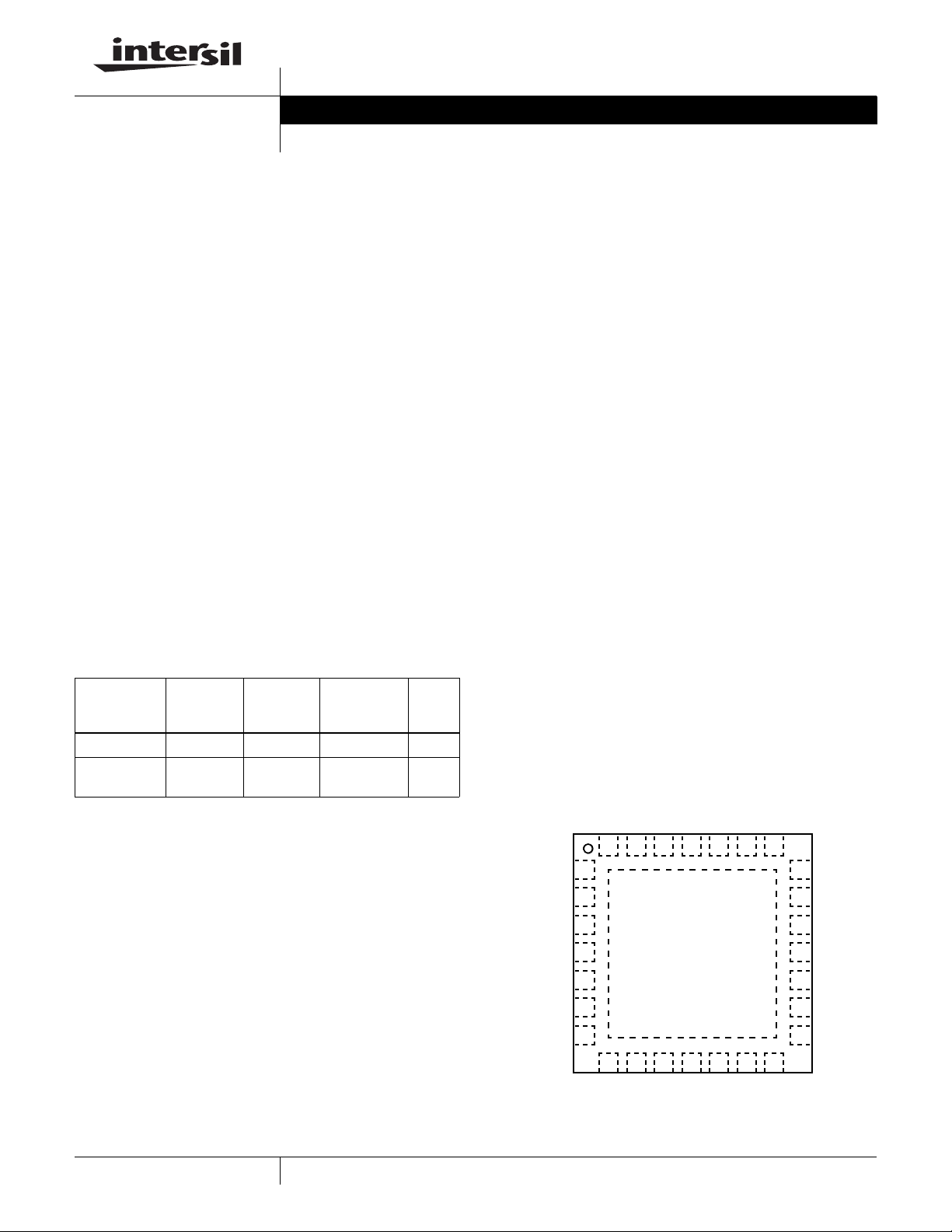
Pinout
ISL6257 (28 LD QFN)
TOP VIEW
DCSET
EN
CELLS
ICOMP
VCOMP
FB
VREF
CHLIM
ACSET
VDD
28 27 26 25 24 23 22
1
2
3
4
5
6
7
8 9 10 11 12 13 14
GND
VADJ
ACLIM
DCPRN
ACPRN
VDDP
CSON
BOOT
21
CSOP
20
CSIN
CSIP
19
18
SGATE
17
BGATE
PHASE
16
UGATE
15
DCIN
PGND
PGND
PGND
LGATE
1
CAUTION: These devices are sensitive to electrostatic discharge; follow proper IC Handling Procedures.
1-888-INTERSIL or 1-888-468-3774
| Intersil (and design) is a registered trademark of Intersil Americas Inc.
All other trademarks mentioned are the property of their respective owners.
Copyright Intersil Americas Inc. 2006-2007. All Rights Reserved
Page 2
ISL6257
Absolute Maximum Ratings Thermal Information
DCIN, CSIP, CSON to GND. . . . . . . . . . . . . . . . . . . . .-0.3V to +28V
CSIP-CSIN, CSOP-CSON. . . . . . . . . . . . . . . . . . . . . -0.3V to +0.3V
CSIP-SGATE, CSIP-BGATE . . . . . . . . . . . . . . . . . . . . .-0.3V to 16V
PHASE to GND . . . . . . . . . . . . . . . . . . . . . . . . . . . . . . . . -7V to 30V
BOOT to GND . . . . . . . . . . . . . . . . . . . . . . . . . . . . . . .-0.3V to +35V
BOOT to VDDP . . . . . . . . . . . . . . . . . . . . . . . . . . . . . . . . -2V to 28V
ACLIM, ACPRN, CHLIM, DCPRN, VDD to GND. . . . . . .-0.3V to 7V
BOOT-PHASE, VDDP-PGND . . . . . . . . . . . . . . . . . . . . . -0.3V to 7V
ACSET and DCSET to GND (Note 1) . . . . . . . -0.3V to VDD + 0.3V
FB, ICOMP, VCOMP to GND. . . . . . . . . . . . . . -0.3V to VDD + 0.3V
VREF, CELLS to GND . . . . . . . . . . . . . . . . . . . -0.3V to VDD + 0.3V
EN, VADJ, PGND to GND . . . . . . . . . . . . . . . . -0.3V to VDD + 0.3V
UGATE. . . . . . . . . . . . . . . . . . . . . . . . PHASE-0.3V to BOOT + 0.3V
LGATE. . . . . . . . . . . . . . . . . . . . . . . . . PGND-0.3V to VDDP + 0.3V
PGND to GND . . . . . . . . . . . . . . . . . . . . . . . . . . . . . . -0.3V to +0.3V
CAUTION: Stresses above those listed in “Absolute Maximum Ratings” may cause permanent damage to the device. This is a stress only rating and operation of the
device at these or any other conditions above those indicated in the operational sections of this specification is not implied.
NOTES:
1. ACSET and DCSET may be operated 1V below GND if the current through ACSET and DCSET is limited to less than 1mA.
is measured in free air with the component mounted on a high effective thermal conductivity test board with “direct attach” features. See T ech
2. θ
JA
Brief TB379.
3. For θ
, the “case temp” location is the center of the exposed metal pad on the package underside.
JC
Thermal Resistance θ
(°C/W) θJC (°C/W)
JA
QFN Package (Notes 2, 3). . . . . . . . . . 39 9.5
QSOP Package (Note 2) . . . . . . . . . . . 80 NA
Junction Temperature Range. . . . . . . . . . . . . . . . . .-10°C to +150°C
Operating Temperature Range . . . . . . . . . . . . . . . .-10°C to +100°C
Storage Temperature. . . . . . . . . . . . . . . . . . . . . . . .-65°C to +150°C
Lead Temperature (soldering, 10s) . . . . . . . . . . . . . . . . . . . .+300°C
Electrical Specifications DCIN = CSIP = CSIN = 18V, CSOP = CSON = 12V, ACSET = DCSET = 1.5V, ACLIM = VREF,
VADJ=Floating, EN=VDD=5V, BOOT-PHASE=5.0V, GND=PGND=0V, C
T
= -10°C to +100°C, TJ≤+125°C, unless otherwise noted.
A
PARAMETER TEST CONDITIONS MIN TYP MAX UNITS
SUPPLY AND BIAS REGULATOR
DCIN Input Voltage Range 725V
DCIN Quiescent Current EN = VDD or GND, 7V ≤ DCIN ≤ 25V 1.4 3 mA
Battery Leakage Current (Note 4) DCIN = 0, no load 3 10 µA
VDD Output Voltage/Regulation 7V ≤ DCIN ≤ 25V, 0 ≤ I
≤ 30mA 4.925 5.075 5.225 V
VDD
VDD Undervoltage Lockout Trip Point VDD Rising 4.0 4.4 4.6 V
Hysteresis 150 250 400 mV
Reference Output Voltage VREF 0 ≤ I
≤ 300µA 2.365 2.39 2.415 V
VREF
FB Feedback Voltage 2.065 2.1 2.12 V
Battery Charge Voltage Accuracy CSON = 16.8V, CELLS = VDD, VADJ = Float -0.5 0.5 %
CSON = 12.6V, CELLS = GND, VADJ = Float -0.5 0.5 %
CSON = 8.4V, CELLS = Float, VADJ = Float -0.5 0.5 %
CSON = 17.64V, CELLS = VDD, VADJ = VREF -0.5 0.5 %
CSON = 13.23V, CELLS = GND, VADJ = VREF -0.5 0.5 %
CSON = 8.82V, CELLS = Float, VADJ = VREF -0.5 0.5 %
CSON = 15.96V, CELLS = VDD, VADJ = GND -0.5 0.5 %
CSON = 11.97V, CELLS = GND, VADJ = GND -0.5 0.5 %
CSON = 7.98V, CELLS = Float, VADJ = GND -0.5 0.5 %
TRIP POINTS
ACSET Threshold 1.24 1.26 1.28 V
ACSET Input Bias Current Hysteresis 2.2 3.4 4.4 µA
ACSET Input Bias Current ACSET ≥ 1.26V 2.2 3.4 4.4 µA
VDD
=1µF, I
VDD
=0mA,
2
FN9288.2
January 17, 2007
Page 3
ISL6257
Electrical Specifications DCIN = CSIP = CSIN = 18V, CSOP = CSON = 12V, ACSET = DCSET = 1.5V, ACLIM = VREF,
VADJ=Floating, EN=VDD=5V, BOOT-PHASE=5.0V, GND=PGND=0V, C
T
= -10°C to +100°C, TJ≤+125°C, unless otherwise noted. (Continued)
A
PARAMETER TEST CONDITIONS MIN TYP MAX UNITS
ACSET Input Bias Current ACSET < 1.26V -1 0 1 µA
DCSET Threshold 1.24 1.26 1.28 V
DCSET Input Bias Current Hysteresis 2.2 3.4 4.4 µA
DCSET Input Bias Current DCSET ≥ 1.26V 2.2 3.4 4.4 µA
DCSET Input Bias Current DCSET < 1.26V -1 0 1 µA
OSCILLATOR
Frequency 245 300 355 kHz
PWM Ramp Voltage (peak-peak) CSIP = 18V 1.6 V
CSIP = 11V 1 V
SYNCHRONOUS BUCK REGULATOR
Maximum Duty Cycle 97 99 99.6 %
UGATE Pull-Up Resistance BOOT - PHASE = 5V, 500mA source current 1.8 3.0 Ω
UGATE Source Current BOOT - PHASE = 5V, BOOT-UGATE = 2.5V 1.0 A
UGATE Pull-Down Resistance BOOT - PHASE = 5V, 500mA sink current 1.0 1.8 Ω
UGATE Sink Current BOOT- PHASE = 5V, UGATE - PHASE = 2.5V 1.8 A
LGATE Pull-Up Resistance VDDP - PGND = 5V, 500mA source current 1.8 3.0 Ω
LGATE Source Current VDDP - PGND = 5V, VDDP - LGATE = 2.5V 1.0 A
LGATE Pull-Down Resistance VDDP - PGND = 5V, 500mA sink current 1.0 1.8 Ω
LGATE Sink Current VDDP - PGND = 5V, LGATE = 2.5V 1.8 A
Dead Time Falling UGATE to rising LGATE or
CHARGING CURRENT SENSING AMPLIFIER
Input Common-Mode Range 0 18 V
Input Offset Voltage Guaranteed by design -1.5 0 1.5 mV
Input Bias Current at CSOP 5 < CSOP < 18V 0.25 2 µA
Input Bias Current at CSON 5 < CSON < 18V 50 100 µA
CHLIM Input Voltage Range 0 3.6 V
CSOP to CSON Full-Scale Current Sense
Voltage
CHLIM Input Bias Current CHLIM = GND or 3.3V, DCIN = 0V -1 1 µA
CHLIM Power-Down Mode Threshold
Voltage
CHLIM Power-Down Mode Hysteresis
Voltage
ADAPTER CURRENT SENSING AMPLIFIER
Input Common-Mode Range 7 25 V
Input Offset Voltage Guaranteed by design -1.5 1.5 mV
Input Bias Current at CSIP and CSIN
Combined
falling LGATE to rising UGATE
CHLIM = 3.3V (4V<CSON<16.8V) 160 165 170 mV
CHLIM = 2.0V (4V<CSON<16.8V) 97 100 103 mV
CHLIM = 0.6V (4V<CSON<16.8V) 28.5 30.0 31.5 mV
CHLIM = 0.2V (4V<CSON<16.8V) 7.5 10 12.5 mV
CHLIM rising 80 88 95 mV
CSIP = CSIN = 25V 100 130 µA
10 30 ns
15 25 40 mV
VDD
=1µF, I
VDD
=0mA,
3
FN9288.2
January 17, 2007
Page 4
ISL6257
Electrical Specifications DCIN = CSIP = CSIN = 18V, CSOP = CSON = 12V, ACSET = DCSET = 1.5V, ACLIM = VREF,
VADJ=Floating, EN=VDD=5V, BOOT-PHASE=5.0V, GND=PGND=0V, C
T
= -10°C to +100°C, TJ≤+125°C, unless otherwise noted. (Continued)
A
PARAMETER TEST CONDITIONS MIN TYP MAX UNITS
Input Bias Current at CSIN 0 < CSIN < DCIN, Guaranteed by design 0.10 1 µA
ADAPTER CURRENT LIMIT THRESHOLD
CSIP to CSIN Full-Scale Current Sense
Voltage
ACLIM = VREF 97 100 103 mV
ACLIM = Float 72 75 78 mV
ACLIM = GND 47 50 53 mV
ACLIM Input Bias Current ACLIM= VREF 10 16 20 µA
ACLIM = GND -20 -16 -10 µA
VOLTAGE REGULATION ERROR AMPLIFIER
Error Amplifier Transconductance from VFB
to VCOMP
CURRENT REGULATION ERROR AMPLIFIER
Charging Current Error Amplifier
Transconductance
Adapter Current Error Amplifier
Transconductance
from V
from V
to ICOMP 50 µA/V
CA2
to ICOMP 50 µA/V
CA1
BATTERY CELL SELECTOR
CELLS Input Voltage for 4 Cell Select 4.3 V
CELLS Input Voltage for 3 Cell Select 2V
CELLS Input Voltage for 2 Cell Select 2.1 4.2 V
MOSFET DRIVER
BGATE Pull-Up Current CSIP - BGATE = 3V 10 30 45 mA
BGATE Pull-Down Current CSIP - BGATE = 5V 2.7 4.0 5.0 mA
CSIP - BGATE Voltage High 8 9.6 11 V
CSIP - BGATE Voltage Low -50 0 50 mV
DCIN - CSON Threshold for CSIP-BGATE
DCIN = 12V, CSON Rising -100 0 100 mV
Going High
DCIN - CSON Threshold Hysteresis 250 300 400 mV
SGATE Pull-Up Current CSIP - SGATE = 3V 7 12 15 mA
SGATE Pull-Down Current CSIP - SGATE = 5V 50 160 370 µA
CSIP - SGATE Voltage High 8 9 11 V
CSIP - SGATE Voltage Low -50 0 50 mV
CSIP - CSIN Threshold for CSIP - SGATE
2.5 8 13 mV
Going High
CSIP - CSIN Threshold Hysteresis 1.3 5 8 mV
LOGIC INTERFACE
EN Input Voltage Range 0VDDV
EN Threshold Voltage Rising 1.030 1.06 1.100 V
Falling 0.985 1.000 1.025 V
Hysteresis 30 60 90 mV
EN Input Bias Current EN = 2.5V 1.8 2.0 2.2 µA
ACPRN Sink Current ACPRN = 0.4V 3 8 11 mA
ACPRN Leakage Current ACPRN = 5V -0.5 0.5 µA
VDD
=1µF, I
VDD
=0mA,
240 µA/V
4
FN9288.2
January 17, 2007
Page 5
ISL6257
Electrical Specifications DCIN = CSIP = CSIN = 18V, CSOP = CSON = 12V, ACSET = DCSET = 1.5V, ACLIM = VREF,
VADJ=Floating, EN=VDD=5V, BOOT-PHASE=5.0V, GND=PGND=0V, C
T
= -10°C to +100°C, TJ≤+125°C, unless otherwise noted. (Continued)
A
PARAMETER TEST CONDITIONS MIN TYP MAX UNITS
DCPRN Sink Current DCPRN = 0.4V 3 8 11 mA
DCPRN Leakage Current DCPRN = 5V -0.5 0.5 µA
CSON to GND resistance CSON = 12.6V 315 380 485 kΩ
Thermal Shutdown Temperature 150 °C
Thermal Shutdown Temperature Hysteresis 25 °C
NOTE:
4. This is the sum of currents in these pins (CSIP, CSIN, BGATE, BOOT, UGATE, PHASE, CSOP, CSON) all tied to 16.8V . No current in pins EN,
ACSET, DCSET, VADJ, CELLS, ACLIM, CHLIM.
VDD
=1µF, I
VDD
=0mA,
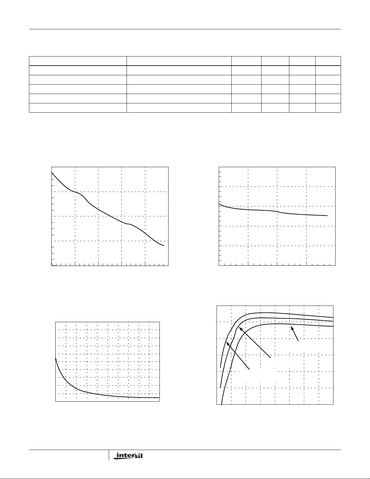
Typical Operating Performance DCIN = 20V, 4S2P Li-Battery, T
0.6
0.3
0.0
-0.3
VDD LOAD REGULATION ACCURACY(%)
-0.6
10
(%)
|
ACCURACY
|
150 5 10 20 40
LOAD CURRENT (mA)
FIGURE 1. VDD LOAD REGULATION
9
8
7
6
5
4
3
2
1
0
0
10 20 30 40 50 60 70 80 90
CSIP-CSIN (mV)
100
VREF LOAD REGULATION ACCURACY(%)
EFFICIENCY (%)
= +25°C, unless otherwise noted.
A
0.10
0.08
0.06
0.04
0.02
0.00
0 100 200 300 400
LOAD CURRENT (μA)
FIGURE 2. VREF LOAD REGULATION
100
96
92
88
84
80
76
VCSON = 16.8V
VCSON = 12.6V
3 CELLS
4 CELLS
1.50 0.5 1.0 2.0 2.5 3.0 3.5 4.0
LOAD CURRENT (A)
VCSON = 8.4V
2 CELLS
FIGURE 3. ACCURACY vs AC ADAPTER CURRENT
5
FIGURE 4. SYSTEM EFFICIENCY vs CHARGE CURRENT
FN9288.2
January 17, 2007
Page 6
A
A
ISL6257
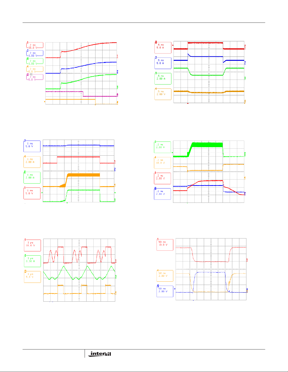
Typical Operating Performance DCIN = 20V, 4S2P Li-Battery, T
DCIN
DCIN
10V/div
10V/div
ACSET
ACSET
1V/div
1V/div
DCSET
DCSET
1V/div
1V/div
DCPRN
DCPRN
5V/div
5V/div
ACPRN
ACPRN
5V/div
5V/div
FIGURE 5. AC AND DC ADAPTER DETECTION
CSON
CSON
5V/div
5V/div
EN
EN
5V/div
5V/div
INDUCTOR
INDUCTOR
CURRENT
CURRENT
2A/div
2A/div
CHARGE
CHARGE
CURRENT
CURRENT
2A/div
2A/div
= +25°C, unless otherwise noted. (Continued)
A
LOAD STEP: 0-4A
CHARGE CURRENT: 3A
C ADAPTER CURRENT LIMIT: 5.15A
FIGURE 6. LOAD TRANSIENT RESPONSE
BATTERY
BATTERY
REMOVAL
REMOVAL
VCOMP
VCOMP
ICOMP
ICOMP
BATTERY
BATTERY
INSERTION
INSERTION
LOAD
CURRENT
5A/div
DAPTER
CURRENT
5A/div
CHARGE
CURRENT
2A/div
BATTERY
VOLTAGE
2V/div
INDUCTOR
INDUCTOR
CURRENT
CURRENT
2A/div
2A/div
CSON
CSON
10V/div
10V/div
VCOMP
VCOMP
2V/div
2V/div
ICOMP
ICOMP
2V/div
2V/div
FIGURE 7. CHARGE ENABLE AND SHUTDOWN FIGURE 8. BATTERY INSERTION AND REMOVAL
CHLIM=0.2V
CHLIM=0.2V
CSON=8V
CSON=8V
PHASE
PHASE
PHASE
10V/div
10V/div
10V/div
INDUCTOR
INDUCTOR
INDUCTOR
CURRENT
CURRENT
CURRENT
1A/div
1A/div
1A/div
UGATE
UGATE
UGATE
5V/div
5V/div
5V/div
FIGURE 9. SWITCHING WAVE FORMS IN DISCONTINUOUS
CONDUCTION MODE (DIODE EMULATION)
FIGURE 10. SWITCHING WAVE FORMS IN CONTINUOUS
CONDUCTION MODE
PHASE
PHASE
10V/div
10V/div
UGATE
UGATE
2V/div
2V/div
LGATE
LGATE
2V/div
2V/div
6
FN9288.2
January 17, 2007
Page 7
E
T
y
ISL6257
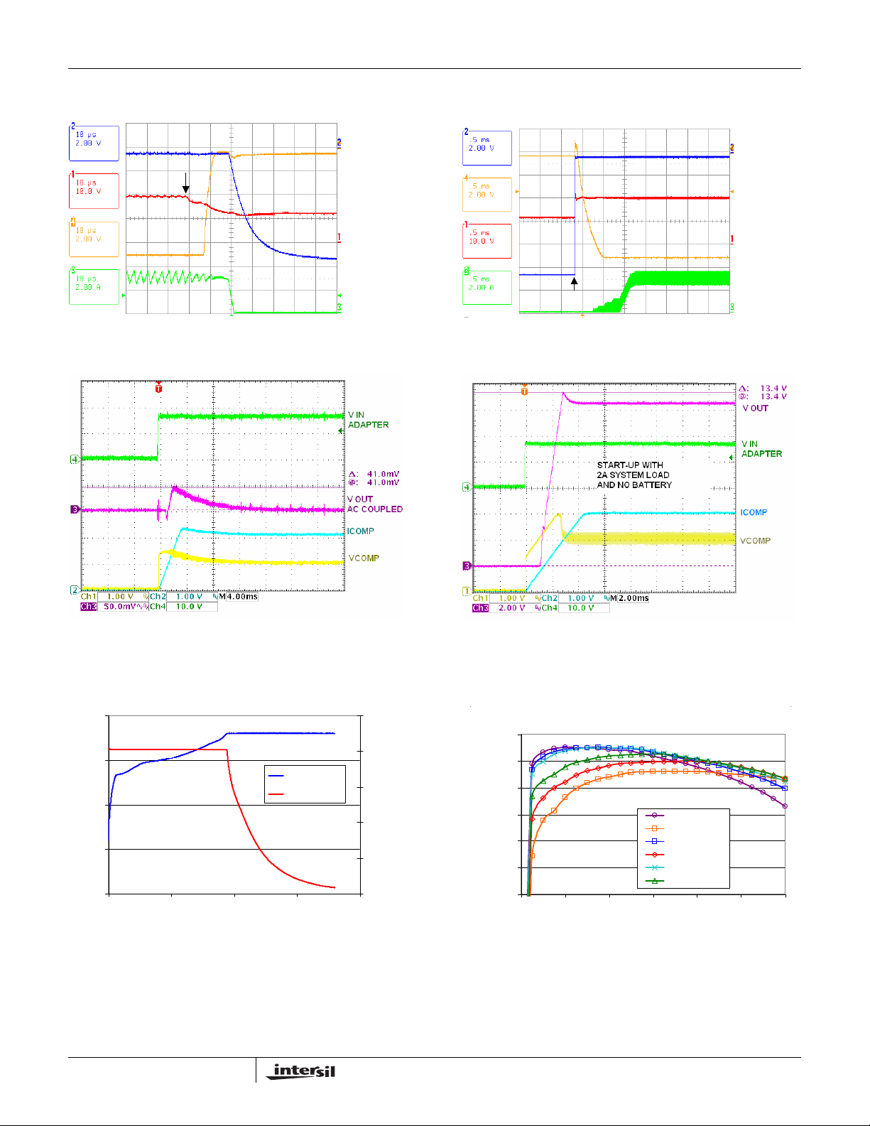
Typical Operating Performance DCIN = 20V, 4S2P Li-Battery, T
SGATE-CSIP
SGATE-CSIP
SGATE-CSIP
2V/div
2V/div
ADAPTER REMOVAL
ADAPTER REMOVAL
FIGURE 11. ADAPTER REMOVAL
2V/div
SYST EM BUS
SYST EM BUS
SYST EM BUS
VOLTAGE
VOLTAGE
VOLTAGE
10V/div
10V/div
10V/div
BGATE-CSIP
BGATE-CSIP
BGATE-CSIP
2V/div
2V/div
2V/div
INDUCTOR
INDUCTOR
INDUCTOR
CURRENT
CURRENT
CURRENT
2A/div
2A/div
2A/div
= +25°C, unless otherwise noted. (Continued)
A
ADAPTER INSERTION
ADAPTER INSERTION
FIGURE 12. ADAPTER INSERTION
BGATE-CSIP
BGATE-CSIP
BGATE-CSIP
2V/div
2V/div
2V/div
SYSTEM BUS
SYSTEM BUS
SYSTEM BUS
VOLTAGE
VOLTAGE
VOLTAGE
10V/div
10V/div
10V/div
SGATE-CSIP
SGATE-CSIP
SGATE-CSIP
2V/div
2V/div
2V/div
INDUCTOR
INDUCTOR
INDUCTOR
CURRENT
CURRENT
CURRENT
2A/div
2A/div
2A/div
FIGURE 13. ADAPTER INSERTION WITH A CHARGED
BATTERY
FIGURE 14. ADAPTER INSERTION WITH NO BATTERY AND A
2A SYSTEM LOAD
ISL6257 CHARGE CURVES
13
12
V ba ttery
11
BATTERY VOLTAG
10
9
0 50 100 150 200
TIM E (MINUTES)
FIGURE 15. BATTERY CHARGE VOLTAGE AND CURRENT
I batter
2.5
2.0
1.5
1.0
0.5
0.0
100%
95%
90%
85%
Efficiency
BATTERY CURREN
80%
75%
10Vin-8.4Vout
25Vin-8.4Vout
15Vin-12.6Vout
25Vin-12.6Vout
20Vin-16.8Vout
25Vin-16.8Vout
70%
024681012
Load Current (Amps)
FIGURE 16. EFFICIENCY VS LOAD CURRENT
Efficiency vs load current
7
FN9288.2
January 17, 2007
Page 8

A
ISL6257
Typical Operating Performance DCIN = 20V, 4S2P Li-Battery, T
18
16
14
12
10
8
Vout (V)
6
4
2
0
024681012
dapt er Current
Limit Mode
System Load Current (Amps)
Line and Load
Regulation
10Vin-8.4Vout
15Vin-8.4Vout
20Vin-8.4Vout
25Vin-8.4Vout
15Vin-12.6Vout
20Vin-12.6Vout
25Vin-12.6Vout
20Vin-16.8Vout
25Vin-16.8Vout
FIGURE 17. LINE AND LOAD REGULATION IN NVDC MODE
Functional Pin Descriptions
BOOT
Connect BOOT to a 0.1µF ceramic capacitor to PHASE pin
and connect to the cathode of the bootstrap Schottky diode.
UGATE
UGATE is the high-side MOSFET gate drive output.
SGATE
SGATE is the AC adapter power source select output. The
SGATE pin drives an external P-MOSFET used to switch to
AC adapter as the system power source.
BGATE
Battery power source select output. This pin drives an
external P-channel MOSFET used to switch the battery as
the system power source in non Narrow VDC systems.
When the voltage at CSON pin is higher than the AC adapter
output voltage at DCIN, BGATE is driven to low and selects
the battery as the power source. In Narrow VDC systems
BGATE should be unconnected.
LGATE
LGATE is the low-side MOSFET gate drive output; swing
between 0V and VDDP.
PHASE
The Phase connection pin connects to the high-side
MOSFET source, output inductor, and low-side MOSFET
drain.
CSOP/CSON
CSOP/CSON is the battery charging current sensing
positive/negative input. The differential voltage across CSOP
and CSON is used to sense the battery charging current,
and is compared with the charging current limit threshold to
regulate the charging current. The CSON pin is also used as
the battery feedback voltage to perform voltage regulation.
0.6%
0.4%
0.2%
0.0%
-0.2%
Vout relative to Vout at 0 Load
-0.4%
-0.6%
FIGURE 18. LINE AND LOAD REGULA TION IN NVDC MODE
CSIP/CSIN
CSIP/CSIN is the AC adapter current sensing
positive/negative input. The differential voltage across CSIP
and CSIN is used to sense the AC adapter current, and is
compared with the AC adapter current limit to regulate the
AC adapter current.
GND
GND is an analog ground.
DCIN
The DCIN pin is the input of the internal 5V LDO. Connect it
to the AC adapter output. Connect a 0.1µF ceramic
capacitor from DCIN to CSON.
ACSET
ACSET is an AC adapter detection input. Connect to a
resistor divider from the AC adapter output.
ACPRN
Open-drain output signals AC adapter is present. ACPRN
pulls low when ACSET is higher than 1.26V and pulled high
when ACSET is lower than 1.26V.
DCSET
DCSET is a lower voltage adapter detection input (like
aircraft power 15V). Allows the adapter to power the system
where battery charging has been disabled.
DCPRN
Open-drain output signals DC adapter is present. DCPRN
pulls low when DCSET is higher than 1.26V and pulled high
when DCSET is lower than 1.26V.
EN
EN is the Charge Enable input. Connecting EN to high
enables the charge control function; connecting EN to low
disables charging functions. Use with a thermistor to detect
a hot battery and suspend charging.
= +25°C, unless otherwise noted. (Continued)
A
Line and Load
Regulation (%)
Adapter Cur r ent
Limit M ode
024681012
System Load Current (Amps)
AS A PERCENTAGE OF NO LOAD VOLTAGE
10Vin-8.4Vout
15Vin-8.4Vout
20Vin-8.4Vout
25Vin-8.4Vout
15Vin-12.6Vout
20Vin-12.6Vout
25Vin-12.6Vout
20Vin-16.8Vout
25Vin-16.8Vout
upper limit
lowerlimit
8
FN9288.2
January 17, 2007
Page 9

ISL6257
FB
The negative feedback of the voltage amplifier which sets
the output voltage at CSON. An internal resistor divider from
CSON adjusts the voltage feedback signal in the ratio of 6:1
for CELLS = GND, 8:1 for CELLS = VDD and 4:1 for
CELLS = float.
PGND
PGND is the power ground. Connect PGND to the source of
the low-side MOSFET.
VDD
VDD is an internal LDO output to supply IC analog circuit.
Connect a 1μF ceramic capacitor to ground.
VDDP
VDDP is the supply voltage for the low-side MOSFET gate
driver. Connect a 4.7Ω resistor to VDD and a 1μF ceramic
capacitor to power ground.
ICOMP
ICOMP is a current loop error amplifier output.
VCOMP
VCOMP is a voltage loop amplifier output.
CELLS
This pin is used to select the battery voltage. CELLS = VDD
for a 4S battery pack, CELLS = GND for a 3S battery pack,
CELLS = Float for a 2S battery pack.
VADJ
VADJ adjusts battery regulation voltage. VADJ = VREF for
4.2V + 5% per cell; VADJ = Floating for 4.2V per cell;
VADJ= GND for 4.2V - 5% per cell. Connect to a resistor
divider to program the desired battery cell voltage between
4.2V - 5% and 4.2V + 5%.
CHLIM
CHLIM is the battery charge current limit set pin.CHLIM input
voltage range is 0.1V to 3.6V. When CHLIM = 3.3V, the set
point for CSOP - CSON is 165mV. The charger shuts down if
CHLIM is forced below 88mV.
ACLIM
ACLIM is the adapter current limit set pin. ACLIM = VREF for
100mV, ACLIM = Floating for 75mV, and ACLIM = GND fo r
50mV. Connect a resistor divider to program the adapter
current limit threshold between 50mV and 100mV.
VREF
VREF is a 2.39V reference output pin. It is internally
compensated. Do not connect a decoupling capacitor.
9
FN9288.2
January 17, 2007
Page 10
ISL6257
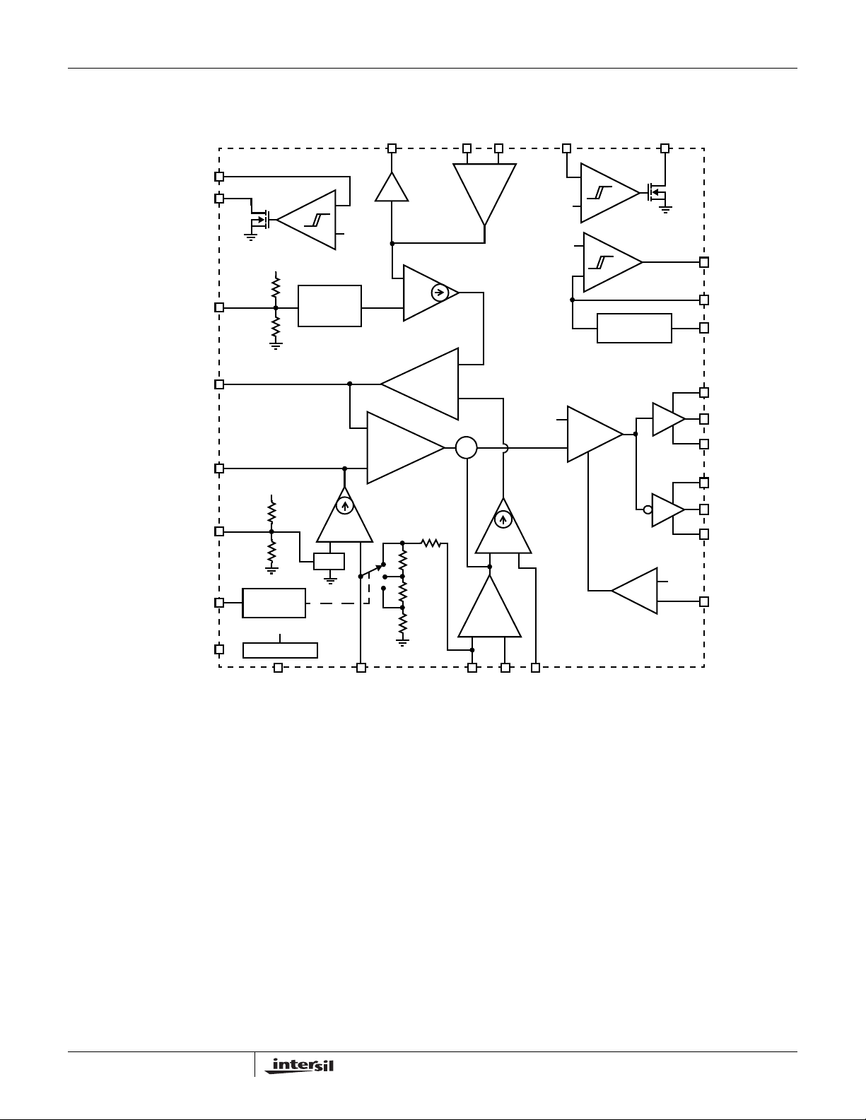
SGATE CSIP CSIN DCSET DCPRN
ACSET
ACPRN
ACLIM
ICOMP
VCOMP
VADJ
CELLS
VREF
VREF
152kΩ
152kΩ
VREF
514kΩ
514kΩ
VOLTAGE
SELECTOR
REFERENCE
VDD
+
-
ADAPTER
CURRENT
LIMIT SET
gm1
+
2.1V
1.26V
-
MIN
VOLTAGE
BUFFER
-
gm3
+
MIN
CURRENT
BUFFER
288kΩ
32kΩ
16kΩ
48kΩ
+
Σ
-
X19.9
CA1
CA2
X19.9
-
1.26V
CSON
+
-
-
BGATE
+
DCIN
LDO
REGULATOR
300kHz
RAMP
-
PWM
+
gm2
+
-
1.065V
-
+
VDD
BOOT
UGATE
PHASE
VDDP
LGATE
PGND
EN
+
10
GND
FB CSIP
FIGURE 19. FUNCTIONAL BLOCK DIAGRAM
CSOP
CHLIM
FN9288.2
January 17, 2007
Page 11

ADAPTER
ISL6257
R
8
100kΩ
1%
R
9
11.5kΩ
1%
HOST
VCC
DIGITAL INPUT
DIGITAL INPUT
DIGITAL OUTPUT
130kΩ
10.2kΩ
R
100kΩ
R
3KΩ
C
1
470pF
5
R
1%
R
1%
1
8
9
CSON
R
56kΩ
C
7
1μF
R
16
100kΩ
33nF
2
VDD
Q
5
0.1μF
CSON
DCIN
ACSET
DCSET
VDDP
R
20
4.7Ω
C
9
ISL6257
VDD
1μF
ACPRN
DCPRN
EN
C
6
ICOMP
C
2
VCOMP
1nF
FB
SGATE
CSIP
CSIN
BOOT
UGATE
PHASE
LGATE
PGND
CSOP
CSON
BGATE
Q
3
C
F2
1μF
R
F2
VDDP
D
2
C
24
0.1μF
18Ω
R
S2
20mΩ
Q
1
C
21
22μF
L
4.7μH
SYSTEM LOAD
C
o
R
S1
330μF
BAT+
Q
C
10μF
10
BAT -
6
C
1μF
Q
2
D
1
OPTIONAL
R
F1
F1
2.2Ω
10mΩ
A/D OUTPUT
A/D OUTPUT
BATTERY
ISOLATION FET
SCL
SDA
A/D INPUT
GND
ACLIM
FLOATING
4.2V/CELL
VREF
CHLIM
VADJ
CELLS
GND
FIGURE 20. ISL6257 TYPICAL NVDC APPLICATION CIRCUIT WITH µP CONTROL
3S2P
BATTERY
PACK
SCL
SDA
TEMP
11
FN9288.2
January 17, 2007
Page 12

ISL6257
Theory of Operation
Introduction
The ISL6257 includes all of the functions necessary to
charge 2 to 4 cell Li-Ion and Li-polymer batteries. A high
efficiency synchronous buck converter is used to control the
charging voltage and charging current up to 10A. The
ISL6257 has input current limiting and analog inputs for
setting the charge current and charge voltage; CHLIM inputs
are used to control charge current. VADJ and CELLS inputs
are used to control charge voltage.
The ISL6257 charges the battery with constant charge current
(set by the CHLIM input) until the battery voltage rises to a
programmed charge voltage (set by the VADJ and CELLS
input) then the charger begins to operate in a constant volt age
mode. The charger also drives an adapter isolation P-channel
MOSFET on SGA TE to efficiently switch in the adapter suppl y.
The EN input allows shutdown of the charger through a
command from a micro-controller. It also uses EN to safely
shutdown the charger when the battery is in extremely hot
conditions. Figure 19 shows the IC functional block diagram.
The synchronous buck converter uses external N-channel
MOSFETs to convert the input voltage to the required
charging current and charging voltage. Figure 20 shows the
ISL6257 typical application circuit which uses a
micro-controller to adjust the charging current set by CHLIM
input for aircraft power applications. The voltage at CHLIM
and the value of R11 sets the charging current. The DC/DC
converter generates the control signals to drive two external
N-channel MOSFETs to regulate the voltage and current set
by the ACLIM, CHLIM, VADJ and CELLS inputs.
The ISL6257 features a voltage regulation loop (VCOMP)
and two current regulation loops (ICOMP). The VCOMP
voltage regulation loop moni to rs CSON to ensure that its
voltage never exceeds the battery charge voltage set by
VADJ and CELLS. The ICOMP current regulation loops
regulate the battery charging current delivered to the battery
to ensure that it never exceeds the charging current limit set
by CHLIM; and the ICOMP current regulation loops also
regulate the input current drawn from the AC adapter to
ensure that it never exceeds the input current limit set by
ACLIM, and to prevent a system crash and AC adapter
overload.
An adaptive gate drive scheme is used to control the dead
time between two switches. The dead time control circuit
monitors the LGATE output and prevents the upper side
MOSFET from turning on until LGATE is fully off, preventing
cross-conduction and shoot-through. In order for the dead
time circuit to work properly, there must be a low resistance,
low inductance path from the LGATE driver to MOSFET
gate, and from the source of MOSFET to PGND. The
external Schottky diode is between the VDDP pin and BOOT
pin to keep the bootstrap capacitor charged.
Setting the Battery Regulation Voltage
The ISL6257 uses a high-accuracy trimmed band-gap
voltage reference to regulate the battery charging voltage.
The VADJ input adjusts the charger output voltage. The
VADJ control voltage can vary from 0 to VREF, providing a
10% adjustment range (from 4.2V - 5% per cell to 4.2V + 5%
per cell) on CSON regulation voltage. An overall voltage
accuracy of better than 0.5% is achieved.
The per-cell battery termination voltage is a function of the
battery chemistry. Consult the battery manufacturers to
determine this voltage.
• Float VADJ to set the battery voltage
V
• Connect VADJ to VREF to set 4.41V × number of cells,
• Connect VADJ to ground to set 3.99V × number of the
cells.
So, the maximum battery voltage of 17.6V can be achieved.
Note that other battery charge voltages can be set by
connecting a resistor divider from VREF to ground. The resistor
divider should be sized to draw no more than 100µA from
VREF or connect a low impedance voltage source like the D/A
converter in the micro-controller. The programmed battery
voltage per cell can be determined by Equation 1:
V
CELL
An external resistor divider from VREF sets the voltage at
VADJ according to Equation 2:
V
VADJ
=4.2V× number of the cells,
CSON
0.175 V
⋅ 3.99V+=
VADJ
---------------------------------------------------------------------------------------------------------
VREF
=
×
R
top_VADJ
R
bot_VADJ
514kΩ||R
||
+
bot_VADJ
514kΩ
||
514kΩ
(EQ. 1)
(EQ. 2)
PWM Control
The ISL6257 employs a fixed frequency PWM voltage mode
control architecture with a feed-forward function. The
feed-forward function maintains a constant modulator gain of
1 1 to achieve fast line regulation as the buck input voltage
changes. When the battery charge voltage approaches the
input voltage, the DC/DC converter operates in dropout
mode, where there is a timer to prevent the frequency from
dropping into the audible frequency range. It can achieve
duty cycle of up to 99.6%.
12
To minimize accuracy loss due to interaction with VADJ's
internal resistor divider, ensure the AC resistance looking
back into the external resistor divider is less than 25k.
Connect CELLS as shown in Table 1 to charge 2, 3 or 4 Li+
cells. When charging other cell chemistries, use CELLS to
select an output voltage range for the charger. The internal
error amplifier gm1 maintains voltage regulation. The voltage
error amplifier is compensated at VCOMP. The component
values shown in Figure 20 provide suitable performance for
most applications. Individual compensation of the voltage
FN9288.2
January 17, 2007
Page 13

ISL6257
regulation and current-regulation loops allows for optimal
compensation.
TABLE 1. CELL NUMBER PROGRAMMING
CELLS CELL NUMBER
VDD 4
GND 3
Float 2
Setting the Battery Charge Current Limit
The CHLIM input sets the maximum charging current. The
current set by the current sense-resistor connects between
CSOP and CSON. The full-scale differential voltage between
CSOP and CSON is 165mV for CHLIM = 3.3V, so the
maximum charging current is 4.125A for a 40mΩ sensing
resistor. Other battery charge current-sense threshold
values can be set by connecting a resistor divider from
VREF or 3.3V to ground, or by connecting a low impedance
voltage source like a D/A converter in the micro-controller.
Unlike VADJ and ACLIM, CHLIM does not have an internal
resistor divider network. The charge current limit threshold is
given by Equation 3:
165mV
⎛⎞
I
CHG
-----------------
=
⎝⎠
To set the trickle charge current for the dumb charger, an
A/D output controlled by the micro-controller is connected to
CHLIM pin. The trickle charge current is determined by
Equation 4:
165mV
⎛⎞
I
CHG
-----------------
=
⎝⎠
When the CHLIM voltage is below 88mV (typical), it will
disable the battery charge. When choosing the current
sensing resistor, note that the voltage drop across the
sensing resistor causes further power dissipation, reducing
efficiency. However, adjusting CHLIM voltage to reduce the
voltage across the current sense resistor R11 will degrade
accuracy due to the smaller signal to the input of the current
sense amplifier. There is a trade-off between accuracy and
power dissipation. A low pass filter is recommended to
eliminate switching noise. Connect the resistor to the CSOP
pin instead of the CSON pin, as the CSOP pin has lower
bias current and less influence on current-sense accuracy
and voltage regulation accuracy.
V
CHLIM
⎛⎞
---------------------
⎝⎠
R
R
3.3V
1
V
CHLIM trickle,
⎛⎞
---------------------------------------
⎝⎠
1
3.3V
(EQ. 3)
(EQ. 4)
the source must be able to supply the maximum system
current and the maximum charger input current
simultaneously . By using the input current limiter , the current
capability of the AC adapter can be lowered, reducing
system cost.
The ISL6257 limits the battery charge current when the input
current-limit threshold is exceeded, ensuring the battery
charger does not load down the AC adapter voltage. This
constant input current regulation allows the adapter to fully
power the system and prevent the AC adapter from
overloading and crashing the system bus.
An internal amplifier gm3 compares the voltage between
CSIP and CSIN to the input current limit threshold voltage
set by ACLIM. Connect ACLIM to REF, Float and GND for
the full-scale input current limit threshold voltage of 100mV,
75mV and 50mV, respectively, or use a resistor divider from
VREF to ground to set the input current limit as Equation 5:
I
INPUT
V
ACLIM
--------------- -
⋅=
⎝⎠
R
2
VREF
V
VREF
ACLIM
⎛⎞
------------------------------------------------------------------------------------------------------------------
⋅=
⎜⎟
R
⎝⎠
top ACLIM,
0.05+⋅
R
bot ACLIM,
152kΩ||R
||
152kΩ
||
+
bot ACLIM,
152kΩ
(EQ. 5)
0.05
1
⎛⎞
------
When choosing the current sense resistor, note that the
voltage drop across this resistor causes further power
dissipation, reducing efficiency. The AC adapter current
sense accuracy is very important. Use a 1% tolerance
current-sense resistor. The highest accuracy of ±1.5% is
achieved with 100mV current-sense threshold voltage for
ACLIM = VREF, but it has the highest power dissipation. For
example, it has 400mW power dissipation for rated 4A AC
adapter and 1W sensing resistor may have to be used.
±2.5% and ±4.5% accuracy can be achieved with 75mV and
50mV current-sense threshold voltage for ACLIM = Floating
and ACLIM = GND, respectively.
A low pass filter is suggested to eliminate the switching
noise. Connect the resistor to CSIN pin instead of CSIP pin
because CSIN pin has lower bias current and less influence
on the current-sense accuracy.
Setting the Input Current Limit
The total input current from an AC adapter, or other DC
source, is a function of the system supply current and the
battery-charging current. The input current regulator limits
the input current by reducing the charging current, when the
input current exceeds the input current limit set by ACLIM.
System current normally fluctuates as portions of the system
are powered up or down. Without input current regulation,
13
FN9288.2
January 17, 2007
Page 14

ISL6257
AC Adapter Detection
Connect the AC adapter voltage through a resistor divider to
ACSET to detect when AC power is available, as shown in
Figure 20. ACPRN is an open-drain output and is high when
ACSET is less than V
above V
th,rise
. V
th,rise
, and active low when ACSET is
th,fall
and V
are given by Equation 6
th,fall
and Equation 7:
R
⎛⎞
8
V
th rise,
V
th fall,
------
⋅=
1+
⎜⎟
R
⎝⎠
R
⎛⎞
------
⎜⎟
R
⎝⎠
V
9
8
9
ACSET
1+
V
ACSETIhysR8
⋅–⋅=
(EQ. 6)
(EQ. 7)
where:
•I
is the ACSET input bias current hysteresis, and
hys
•V
The hysteresis is I
= 1.24V (min), 1.26V (typ) and 1.28V (max).
ACSET
hysR8
, where I
= 2.2µA (min),
hys
3.4µA (typ) and 4.4µA (ma x).
DC Adapter Detection
Connect the DC input through a resistor divider to DCSET to
detect when lower voltage (i.e. aircraft) DC power is
available. DCPRN is an open-drain output and is high when
DCSET is less than V
above V
th,rise
. V
th,rise
and Equation 9:
R
⎛⎞
24
-------- -
V
th rise
,
1+
⎜⎟
R
⎝⎠
25
, and active low when DCSET is
th,fall
•=
V
and V
DCSET
are given by Equation 8
th,fall
(EQ. 8)
EN can be driven by a thermistor to allow automatic
shutdown of the ISL6257 when the battery pack is hot. Often
an NTC thermistor is included inside the battery pack to
measure its temperature. When connected to the charger,
the thermistor forms a voltage divider with a resistive pull-up
to the VREF. The threshold voltage of EN is 1.0V with 60mV
hysteresis. The thermistor can be selected to have a
resistance vs temperature characteristic that abruptly
decreases above a critical temperature. This arrangement
automatically shuts down the ISL6257 when the battery pack
is above a critical temperature.
Another method for inhibiting charging is to force CHLIM
below 85mV (typ).
Supply Isolation
If the voltage across the adapter sense resistor R2 is
typically greater than 8mV, the P-channel MOSFET
controlled by SGATE is turned on reducing the power
dissipation. If the voltage across the adapter sense resistor
R
is less than 3mV, SGATE turns off the P-channel
2
MOSFET isolating the adapter from the system bus.
Battery Power Source Selection and Aircraft
Power Application
The battery voltage is monitored by CSON. If the battery
voltage measured on CSON is less than the adapter voltage
measured on DCIN, then the P-channel MOSFET controlled
by SGATE is allowed to turn on when the adapter current is
high enough. If it is greater, then the P-channel MOSFET
controlled by SGATE turns off.
V
th fall
,
R
⎛⎞
24
-------- -
1+
⎜⎟
R
⎝⎠
25
V
DCSETIhysR24
–•=
(EQ. 9)
where:
•I
is the DCSET input bias current hysteresis, and
hys
•V
The hysteresis is I
= 1.24V (min), 1.26V (typ) and 1.28V (max).
DCSET
hysR14
, where I
= 2.2µA (min),
hys
3.4µA (typ) and 4.4µA (ma x).
LDO Regulator
VDD provides a 5.0V supply voltage from the internal LDO
regulator from DCIN and can deliver up to 30mA of current.
The MOSFET drivers are powered by VDDP, which must be
connected to VDDP as shown in Figure 20. VDDP connects
to VDD through an external low pass filter. Bypass VDDP
and VDD with a 1µF capacitor.
Shutdown
The ISL6257 features a low-power shutdown mode. Driving
EN low shuts down the ISL6257. In shutdown, the DC/DC
converter is disabled, and VCOMP and ICOMP are pulled to
ground. The ACPRN and DCPRN outputs continue to
function.
When operating on aircraft power it is desirable to disable
charging to minimize loading of the aircraft power systems.
DCIN is usually lower when connected to aircraft power
(15V) than it is when connected AC power (20V). The
DCSET pin provides means of detecting this lower DC input
voltage. If the DC input voltage is below the ACSET
threshold and above the DCET threshold, ACPRN will be
high and DCPRN will be low, and the host may turn off Q
5
(Figure 20) to stop charging the battery.
Short Circuit Protection
Since the battery charger will regulate the charge current to
the limit set by CHLIM, it automatically has short circuit
protection and is able to provide the charge current to wake
up an extremely discharged battery.
Over Temperature Protection
If the die temperature exceeds +150°C, it stops charging.
Once the die temperature drops below +125°C, charging will
start up again.
14
FN9288.2
January 17, 2007
Page 15

ISL6257
Application Information
The following battery charger design refers to the typical
application circuit in Figure 20, where typical battery
configuration of 3S2P is used. This section describes how to
select the external components including the inductor, input
and output capacitors, switching MOSFETs, and current
sensing resistors.
Inductor Selection
The inductor selection has trade-offs between cost, size and
efficiency. For example, the lower the inductance, the
smaller the size, but ripple current is higher. This also results
in higher AC losses in the magnetic core and the windings,
which decrease the system efficiency. On the other hand,
the higher inductance results in lower ripple current and
smaller output filter capacitors, but it has higher DCR (DC
resistance of the inductor) loss, and has slower transient
response. So, the practical inductor design is based on the
inductor ripple current bei ng ±15 % to ± 20% of the maximu m
operating DC current at maximum input voltage. Maximum
ripple is at 50% duty cycle or V
BAT=VIN,MAX
required inductance can be calculated from Equation 10:
R
IN MAX,
-------------------------------------------
L
=
4ISWI
⋅⋅
RIPPLE
Where V
and fSW are the maximum input voltage,
IN,MAX
and switching frequency, respectively.
The inductor ripple current ΔI is found from Equation 11:
RIPPLE
=
LMAX,
I
0.3 I⋅
where the maximum peak-to-peak ripple current is 30% of
the maximum charge current is used.
For V
IN,MAX
f
= 300kHz, the calculated inductance is 4.7µH. Ferrite
s
=19V, V
BAT
= 12.6V, I
L,MAX
cores are often the best choice since they are optimized at
300kHz to 600kHz operation with low core loss. The core
must be large enough not to saturate at the peak inductor
current I
I
PEAKILMAX,
in Equation 12:
Peak
+ I
1
-- -
2
⋅=
RIPPLE
Output Capacitor Selection
The output capacitor in parallel with the battery is used to
absorb the high frequency switching ripple current and
supply very high di/dt load transients. In a Narrow VDC
system the output capacitance is also the bypass
capacitance on the input of the CORE regulator and may be
several hundred µF. The following examples use 330µF with
ESR = 6mΩ.
The RMS value of the output ripple current I
Equation 13:
V
IN MAX,
RMS
---------------------------------
12 L FSW⋅⋅
D1D–()⋅⋅=
I
/2. The
= 10A, and
is given by
rms
(EQ. 10)
(EQ. 11)
(EQ. 12)
(EQ. 13)
where the duty cycle D is the ratio of the output voltage
(battery voltage) over the input voltage for continuous
conduction mode, which is typical operation for the battery
charger. During the battery charge period, the output voltage
varies from its initial battery voltage to the rated battery
voltage. So, the duty cycle change can be in the range of
between 0.5 and 0.88 for the minimum battery voltage of
10V (2.5V/Cell) and the maximum battery voltage of 16.8V.
The maximum RMS value of the output ripple current occurs
at the duty cycle of 0.5 and is expressed as Equation 14:
V
IN MAX,
RMS
=
IN,MAX
-----------------------------------------
412LF
⋅⋅⋅
SW
= 19V, L = 4.7µH, and fs= 300kHz, the
(EQ. 14)
I
For V
maximum RMS current is 0.98A. Ceramic capacitors are
good choices to absorb this current and also has very small
size. Organic polymer capacitors have high capacitance with
small size and have a significant equivalent series
resistance (ESR). Although ESR adds to ripple voltage, it
also creates a high frequency zero that helps the closed loop
operation of the buck regulator.
EMI considerations usually make it desirable to minimize
ripple current in the battery leads. Beads may be added in
series with the battery pack to increase the battery
impedance at 300kHz switching frequency. Switching ripple
current splits between the battery and the output capacitor
depending on the ESR of the output capacitor and battery
impedance. If the ESR of the output capacitor is 10mΩ and
battery impedance is raised to 2Ω with a bead, then only
0.5% of the ripple current will flow in the battery.
MOSFET Selection
The notebook battery charger synchronous buck converter
has the input voltage from the AC adapter output. The
maximum AC adapter output voltage does not exceed 25V.
Therefore, MOSFETs should be used that are rated for 30V
VDS with low r
DS(ON)
at 5V VGS.
The high-side MOSFET must be able to dissipate the
conduction losses plus the switching losses. For the battery
charger application, the input voltage of the synchronous
buck converter is equal to the AC adapter output voltage,
which is relatively constant. The maximum efficiency is
achieved by selecting a high-side MOSFET that has the
conduction losses equal to the switching losses. Switching
losses in the low-side FET are very small. The choice of
low-side FET is a trade off between conduction losses
(r
the low-side FET is 2X the r
) and cost. A good rule of thumb for the r
DS(ON)
DS(ON)
of the high-side FET.
DS(ON)
of
The ISL6257 LGATE gate driver can drive sufficient gate
current to switch most MOSFETs efficiently. However, some
FETs may exhibit cross conduction (or shoot through) due to
current injected into the drain-to-source parasitic capacitor
(C
) by the high dV/dt rising edge at phase node when the
gd
high-side MOSFET turns on. Although LGATE sink current
(1.8A typical) is more than enough to switch the FET off
15
FN9288.2
January 17, 2007
Page 16

ISL6257
quickly, volt age drop s across parasitic impedances between
LGATE and the MOSFET can allow the gate to rise during
the fast rising edge of voltage on the drain. MOSFETs with
low threshold voltage (<1.5V) and low ratio of C
gs/Cgd
(<5)
and high gate resistance (>4Ω) may be turned on for a few
ns by the high dV/dt (rising edge) on their drain. This can be
avoided with higher threshold voltage and C
gs/Cgd
ratio.
Another way to avoid cross conduction is slowing the turn-on
speed of the high-side MOSFET by connecting a resistor
between the BOOT pin and the boot strap cap.
For the high-side MOSFET, the worst-case conduction
losses occur at the minimum input voltage as shown in
Equation 15:
V
OUT
P
Q1 conduction,
-------------- -
V
IN
2
I
BAT
r
DS ON()
⋅⋅=
(EQ. 15)
The optimum efficiency occurs when the switching losses
equal the conduction losses. However, it is difficult to
calculate the switching losses in the high-side MOSFET
since it must allow for difficult-to-quantify factors that
influence the turn-on and turn-off times. These factors
include the MOSFET internal gate resistance, gate charge,
threshold voltage, stray inductance, pull-up and pull-down
resistance of the gate driver. The following switching loss
calculation (Equation 16) provides a rough estimate.
P
Q1 Switching,
1
-- -
V
INILVfsw
2
=
Q
⎛⎞
-----------------------
⎜⎟
I
⎝⎠
gsource,
gd
1
-- -
V
INILPfsw
2
Q
⎛⎞
gd
----------------
++
⎜⎟
I
⎝⎠
gksin,
Q
rrVINfsw
(EQ. 16)
where the following are the peak gate-drive source/sink
current of Q
, respectively:
1
•Qgd: drain-to-gate charge,
: total reverse recovery charge of the body-diode in
•Q
rr
low-side MOSFET,
: inductor valley current,
•I
LV
: Inductor peak current,
•I
LP
•I
g,sink
•Ig,
source
To achieve low switching losses, it requires low drain-to-gate
charge Q
. Generally, the lower the drain-to-gate charge,
gd
the higher the on-resistance. Therefore, there is a trade-off
between the on-resistance and drain-to-gate charge. Good
MOSFET selection is based on the Figure of Merit (FOM),
which is a product of the total gate charge and
on-resistance. Usually, the smaller the value of FOM, the
higher the efficiency for the same application.
For the low-side MOSFET, the worst-case power dissipation
occurs at minimum battery voltage and maximum input
voltage (Equation 17):
V
⎛⎞
P
1
–
⎜⎟
Q2
⎝⎠
OUT
-------------- -
V
IN
2
I
BAT
r
DS ON()
⋅⋅=
(EQ. 17)
Choose a low-side MOSFET that has the lowest possible
on-resistance with a moderate-sized package like the SO-8
and is reasonably priced. The switching losses are not an
issue for the low-side MOSFET because it operates at
zero-voltage-switching.
Choose a Schottky diode in parallel with low-side MOSFET
Q
with a forward voltage drop low enough to prevent the
2
low-side MOSFET Q
body-diode from turning on during the
2
dead time. This also reduces the power loss in the high-side
MOSFET associated with the reverse recovery of the
low-side MOSFET Q
body diode.
2
As a general rule, select a diode with DC current rating equal
to one-third of the load current. One option is to choose a
combined MOSFET with the Schottky diode in a single
package. The integrated packages may work better in
practice because there is less stray inductance due to a
short connection. This Schottky diode is optional and may be
removed if efficiency loss can be tolerated. In addition,
ensure that the required total gate drive current for the
selected MOSFETs should be less than 24mA. So, the total
gate charge for the high-side and low-side MOSFETs is
limited by Equation 18:
1
GATE
where I
f
sw
is the total gate drive current and should be
GATE
GATE
-----------------
≤
Q
less than 24mA. Substituting I
= 24mA and fs= 300kHz
GATE
(EQ. 18)
into Equation 18 yields that the total gate charge should be
less than 80nC. Therefore, the ISL6257 easily drives the
battery charge current up to 8A.
Snubber Design
ISL6257's buck regulator operates in discontinuous current
mode (DCM) when the load current is less than half the
peak-to-peak current in the inductor. After the low-side FET
turns off, the phase voltage rings due to the high impedance
with both FETs off. This can be seen in Figure 9. Adding a
snubber (resistor in series with a capacitor) from the phase
node to ground can greatly reduce the ringing. In some
situations a snubber can improve output ripple and
regulation.
The snubber capacitor should be approximately twice the
parasitic capacitance on the phase node. This can be
estimated by operating at very low load current (100mA) and
measuring the ringing frequency.
16
FN9288.2
January 17, 2007
Page 17

ISL6257
CSNUB and RSNUB can be calculated from Equation 19:
C
SNUB
----------------------------------
= R
2π f
()2L⋅
2
ring
SNUB
=
1
------------------------------------------
2C⋅
⋅
SNUBfring
(EQ. 19)
Input Capacitor Selection
The input capacitor absorbs the ripple current from the
synchronous buck converter, which is given by Equation20:
=
I
RMSIBAT
V
OUTVINVOUT
-----------------------------------------------------------
–()⋅
V
IN
(EQ. 20)
This RMS ripple current must be smaller than the rated RMS
current in the capacitor datasheet. Non-tantalum chemistries
(ceramic, aluminum, or OSCON) are preferred due to their
resistance to power-up surge currents when the AC adapter is
plugged into the battery charger. For notebook battery charger
applications, it is recommend that ceramic capacitors or
polymer capacitors from Sanyo be used due to their small size
and reasonable cost.
Table 2 shows the component lists for the typical application
circuit in Figure 20.
TABLE 2. COMPONENT LIST
PARTS PART NUMBERS AND MANUFACTURER
, C1022μF/25V ceramic capacitor, TDK,
C
21
C
12
, C7, C91μF/10V ceramic capacitor, Taiyo Yuden
C
3
C
C
C
C
D
D
Q
Q
Q
Q
Q
R
R
R
R
R
R
R
5
R
R
R
C5750X7R1E226M
, C240.1μF/50V ceramic capacitor
LMK212BJ105MG
1nF ceramic capacitor
2
33nF ceramic capacitor
6
330µF, 6mΩ electrolytic capacitor (system load)
o
470pF ceramic capacitor
1
30V/3A Schottky diode, EC31QS03L (optional)
1
100mA/30V Schottky Diode, Central Semiconductor
2
L4.7μH/10.2A/8.8mΩ, Toko, FDA1254-4R7M
6mΩ/30V, HAT2168HFDS6912A, Fairchild
1
2.5mΩ/30V HAT2165H
2
-30V/30mΩ, Si4835BDY, Siliconix
3
Signal P-channel MOSFET, NDS352AP
5
-30V/30mΩ, Si4835BDY, Siliconix
6
3kΩ, ±1%, (0805)
1
56kΩ, ±1%, (0805)
2
10mΩ, ±1%, LRC-LR2512-01-R010-F, IRC
S1
20mΩ, ±1%, LRC-LR2010-01-R020-F, IRC
S2
18Ω, ±5%, (0805)
F2
2.2Ω, ±5%, (0805)
F1
, R7100kΩ, ±5%, (0805)
130k, ±1%, (0805)
8
10.2kΩ, ±1%, (0805)
9
4.7Ω, ±5%, (0805)
20
TABLE 2. COMPONENT LIST (Continued)
PARTS PART NUMBERS AND MANUFACTURER
R
R
R
100kΩ, ±1%, (0805)
24
11.5kΩ, ±1%, (0805)
15
100kΩ, ±1%, (0805)
16
Loop Compensation Design
ISL6257 has three closed loop control modes. One controls the
output voltage when the battery is fully charged or absent. A
second controls the current into the battery when charging and
the third limits current drawn from the adapter. The charge
current and input current control loops are compensated by a
single capacitor on the ICOMP pin. The voltage control loop is
compensated by a network shown in Figure 23. Descriptions of
these control loops and guidelines for selecting compensation
components will be given in the following sections. Which loop
controls the output is determined by the minimum current buffer
and the minimum voltage buffer shown in Figure 19. These
three loops will be described separately.
Transconductance Amplifiers gm1, gm2 and gm3
ISL6257 uses several transconductance amplifiers (also known
as gm amps). Most commercially available op amps are voltage
controlled voltage sources with gain expressed as
A=V
OUT/VIN
with gain expressed as gm = I
. gm amps are voltage controlled current sources
OUT/VIN
. gm will appear in some
of the equations for poles and zeros in the compensation.
PWM Gain F
m
The Pulse Width Modulator in the ISL6257 converts voltage at
VCOMP (or ICOMP) to a duty cycle by comparing VCOMP to a
triangle wave (duty = VCOMP/V
formed by L and C
voltage (Vo= V
amplitude is proportional to V
convert the duty cycle to a DC output
O
*duty). In ISL6257, the triangle wave
DCIN
DCIN
PP RAMP
). The low-pass filter
. Making the ramp amplitude
proportional to DCIN makes the gain from VCOMP to the
PHASE output a constant 11 and is independent of DCIN.
VDD
RAMP GEN
= VDD/11
V
RAMP
L
-
VCOMP
VCOMP
FIGURE 21. FOR SMALL SIGNAL AC ANALYSIS, THE
+
11
DRIVERS
L
C
R
ESR
R
O
PWM AND POWER STAGE CAN BE
MODELED AS A SIMPLE GAIN OF 11.
C
ESR
O
17
FN9288.2
January 17, 2007
Page 18

ISL6257
Output LC Filter Transfer Functions
The gain from the phase node to the system output and
battery depend entirely on external components. Transfer
function A
A
LC
ω
ESR
PHASE (DEGREES) GAIN (dB)
FIGURE 22. FREQUENCY RESPONSE OF THE LC OUTPUT
(s) is shown in Equation 21 and Equation 22:
LC
s
⎛⎞
------------- -
1
–
⎝⎠
ω
2
-------------------------
ω
DP
1
⋅()
ESRCo
R
BATTERY
= 100mΩ
R
BATTERY
= 50mΩ
ESR
s
Q⋅()
1++
-----------------------
ω
=
DP
FREQUENCY
1
⋅()
LC
o
NO BATTERY
----------------------------------------------------------
=
⎛⎞
s
-----------
⎜⎟
ω
⎝⎠
DP
-----------------------------
=
R
FILTER
QR
o
(EQ. 21)
L
------⋅=
C
o
(EQ. 22)
voltage buffer output equals the voltage on VCOMP. The
voltage control loop is shown in Figure 23.
RAMP GEN
V
= VDD/11
RAMP
-
+
VCOMP
R
FOR SMALL SIGNAL AC ANALYSIS, VOLTAGE SOURCES
ARE SHORT CIRCUITS AND CURRENT SOURCES ARE
OPEN CIRCUITS.
VCOMP
2
R
gm1
2
-
+
11
gm1
DRIVERS
C
2
C
2
-
+
FB
V
REF
=2.1V
PHASE
FB
VDD
PHASE
R
1
R
1
R
4
R
R
CSON
C
1
3
L
C
4
1
R
L
CSON
3
C
O
R
ESR
I
SYSTEM
C
O
R
ESR
R
R
R
BAT
S2
BAT
R
S2
The load resistance R
r
, inductor DCR and the internal resistance of the
DS(ON)
is a combination of MOSFET
O
battery (normally between 50mΩ and 200mΩ) in parallel with
the system. The system load may be modeled as a current
sink in parallel with a resistance. For AC analysis of the
voltage control loop this may be treated as a very high
resistance or an open circuit. The worst case for voltage
mode control is when the battery is absent. This results in
the highest Q of the LC filter and the lowest phase margin.
Voltage Control Loop
The voltage error amplifier controls the output when the
battery is not drawing current and the input current is below
the limit. Under these conditions VCOMP controls the
charger’s output because the 2 current error amplifiers (gm2
and gm3) output their maximum current and charge the
capacitor on ICOMP to its maximum voltage (limited to 1.2V
above VCOMP). With high voltage on ICOMP, the minimum
FIGURE 23. VOLTAGE LOOP COMPENSATOR
18
FN9288.2
January 17, 2007
Page 19

FFF
F
F
ISL6257
The compensation network consists of the voltage error
amplifier gm1 and the compensation network R
C
. R3 and R4 are internal divider resisters that set the DC
2
output voltage. For a 3 cell battery, R
R
= 64kΩ. The equations below relate the compensation
4
= 320kΩ and
3
, C1, R2 and
1
network’s poles, zeros and gain to the components in Figure
20. Figure 24 shows an asymptotic Bode plot of the DC/DC
converter’s gain vs. frequency. It is strongly recommended
that F
1/2*F
is approximately 1/4*FDP and FZ2 is approximately
Z1
.
DP
60
50
40
30
20
10
GAIN (dB)
0
-10
-20
-30
-40
0.01 0.1 1 10 100 1000
DP
Z1
Z2
FREQUENCY (kHz)
Loop
Modulator
Compensator
P1
ZESR
FIGURE 24. ASYMPTOTIC BODE PLOT OF THE VOLTAGE
CONTROL LOOP GAIN
Compensation Break Frequency Equations
---------------------------------------------------
F
=
Z1
----------------------------------------------------------
F
=
Z2
⎛⎞
⎜⎟
⎝⎠
------------------------------
=
F
DP
F
=
ESR
1
2π C
+()⋅⋅()
1R1R3
1
⎧⎫
1
2π C
⋅⋅
2R2
1
2π LC
-----------------------------------------
⋅⋅()
2π C
---------- -
–
⎨⎬
gm1
⎩⎭
⋅()
o
F
1
oRESR
P1
=
--------------------------------- -
TABLE 3.
CELLS R
2 288kΩ
3 320kΩ
4 336kΩ
1
---------- -
4.17kΩ=
gm1
1
⋅⋅()
2π R
1C1
3
(EQ. 23)
(EQ. 24)
(EQ. 25)
(EQ. 26)
Charge Current Control Loop
When the battery voltage is less than the fully charged
voltage, the voltage error amplifier goes to it’s maximum
output (limited to 1.2V above ICOMP) and the ICOMP
voltage controls the loop through the minimum voltage
buffer. Figure 25 shows the charge current control loop.
L
11
ICOMP
C
ICOMP
PHASE
Σ
gm2
-
CA2
-
+
+
0.25
S
CHLIM
CSOP
+
20
-
CSON
+
C
O
R
ESR
R
F2
C
F2
R
S2
R
BAT
-
FIGURE 25. CHARGE CURRENT LIMIT LOOP
The compensation capacitor (C
amplifier (gm2) a pole at a very low frequency (<<1Hz) and a
a zero at F
. F
is created by the 0.25*CA2 output added to
Z1
Z1
ICOMP. The loop response has another zero due to the
output capacitor’s esr.
A filter should be added between R
to reduce switching noise. The filter roll off frequency should
be between the cross over frequency and the switching
frequency (~100kHz). R
should be small (<10Ω) to
F2
minimize offsets due to leakage current into CSOP.
1
------------------------------
F
=
DP
F
ZESR
F
= gm2 50μAV⁄=
Z1
F
FILTER
⋅()
2π LC
=
--------------------------------------
2π C
o
1
-----------------------------------------
⋅⋅()
2π C
oRESR
4gm2⋅
⋅()
ICOMP
1
-----------------------------------------
=
⋅⋅()
2π C
F2RF2
) gives the error
ICOMP
and CSOP and CSON
S2
(EQ. 27)
(EQ. 28)
(EQ. 29)
(EQ. 30)
19
FN9288.2
January 17, 2007
Page 20

ISL6257
60
F
40
20
0
GAIN (dB)
-20
-40
F
Z1
DP
F
-60
0.01 0.1 1 10 100 1000
FREQUENCY (kHz)
ZESR
Compensator
Modulator
Loop
F
FILTER
FIGURE 26. CHARGE CURRENT LOOP BODE PLOTS
C
should be chosen using Equation 31 to set
ICOMP
F
Z1=FDP
2.5 * F
+40°C depending on F
C
/10. The crossover frequency will be approximately
. The phase margin will be between +10°C and
DP
.
ZESR
4gm2⋅
--------------------------------
=
ICOMP
2π F
DP
10⁄⋅
(EQ. 31)
Adapter Current Limit Control Loop
If the combined battery charge current and system load
current draws current that equals the adapter current limit
set by the ACLIM pin, ISL6257 will reduce the current to the
battery and/or reduce the output voltage to hold the adapter
current at the limit. Figure 17 shows the effect on output
voltage as the load current is swept up beyond the adapter
current limit. Above the adapter current limit the minimum
current buffer equals the output of gm3 and ICOMP controls
the charger output. Figure 27 shows the resulting adapter
current control system.
A filter should be added between R
and CSIP and CSIN to
S1
reduce switching noise. The filter roll off frequency should be
between the cross over frequency and the switching
frequency (~100kHz).
DCIN
R
C
S1
C
F1
ICOMP
R
F1
CSIN
CSIP
ICOMP
11
S
Σ
-
+
20
0.25
CA1
gm3
PHASE
+
-
CA2
-
+
ACLIM
FIGURE 27. ADAPTER CURRENT LIMIT LOOP
L
C
O
R
ESR
CSOP
+
20
-
CSON
+
R
F2
C
R
F2
S2
R
-
The loop response equations, bode plots and the selection
of C
are the same as the charge current control loop
ICOMP
with loop gain reduced by the duty cycle. In other words, if
the duty cycle D = 50%, the loop gain will be 6dB lower than
the loop gain in Figure 26. This gives lower crossover
frequency and higher phase margin in this mode.
PCB Layout Considerations
Power and Signal Layers Placement on the PCB
As a general rule, power layers should be close together,
either on the top or bottom of the board, with signal layers on
the opposite side of the board. As an example, layer
arrangement on a 4-layer board is shown below:
1. Top Layer: signal lines, or half board for signal lines and
the other half board for power lines
2. Signal Ground
3. Power Layers: Power Ground
4. Bottom Layer: Power MOSFET, Inductors and other
Power traces
Separate the power voltage and current flowing path from
the control and logic level signal path. The controller IC will
stay on the signal layer, which is isolated by the signal
ground to the power signal traces.
BAT
20
FN9288.2
January 17, 2007
Page 21

ISL6257
Component Placement
The power MOSFET should be close to the IC so that the
gate drive signal, the LGATE, UGATE, PHASE, and BOOT,
traces can be short.
Place the components in such a way that the area under the
IC has less noise traces with high dV/dt and di/dt, such as
gate signals and phase node signals.
Signal Ground and Power Ground Connection
At minimum, a reasonably large area of copper, which will
shield other noise couplings through the IC, should be used
as signal ground beneath the IC. The best tie-point between
the signal ground and the power ground is at the negative
side of the output capacitor on each side, where there is little
noise; a noisy trace beneath the IC is not recommended.
GND and VDD Pin
At least one high quality ceramic decoupling cap should be
used to cross these two pins. The decoupling cap can be put
close to the IC.
LGATE Pin
This is the gate drive signal for the bottom MOSFET of the
buck converter. The signal going through this trace has both
high dV/dt and high di/dt, and the peak charging and
discharging current is very high. These two traces should be
short, wide, and away from other traces. There should be no
other traces in parallel with these traces on any layer.
PGND Pin
PGND pin should be laid out to the negative side of the
relevant output cap with separate traces.The negative side
of the output capacitor must be close to the source node of
the bottom MOSFET. This trace is the return path of LGA TE.
PHASE Pin
This trace should be short, and positioned away from other
weak signal traces. This node has a very high dV/dt with a
voltage swing from the input voltage to ground. No trace
should be in parallel with it. This trace is also the return path
for UGATE. Connect this pin to the high-side MOSFET
source.
UGATE Pin
This pin has a square shape waveform with high dV/dt. It
provides the gate drive current to charge and discharge the
top MOSFET with high di/dt. This trace should be wide,
short, and away from other traces similar to the LGATE.
BOOT Pin
This pin’s di/dt is as high as the UGATE; therefore, this trace
should be as short as possible.
CSIP, CSIN Pins
The input current sense resistor connects to the CSIP and
CSIN pins through a low pass filter. The traces should be
away and guarded/shielded from the high dV/dt and di/dt
nodes like Phase, Boot.
CSOP, CSON Pins
The charging current sense resistor connects to the CSOP
and the CSON pins through a low pass filter. The traces
should be away and guarded/shielded from the high dV/dt
and di/dt nodes like PHASE, BOOT. In general, the current
sense resistor should be close to the IC.
EN Pin
This pin stays high at enable mode and low at idle mode and
is relatively robust. Enable signals should refer to the signal
ground.
DCIN Pin
This pin connects to AC adapter output voltage, and should
be less noise sensitive.
Copper Size for the Phase Node
The capacitance of PHASE should be kept very low to
minimize ringing. It would be best to limit the size of the
PHASE node copper in strict accordance with the current
and thermal management of the application.
Identify the Power and Signal Ground
The input and output capacitors of the converters, the source
terminal of the bottom switching MOSFET PGND should
connect to the power ground. The other components should
connect to signal ground. Signal and power ground are tied
together at one point.
Clamping Capacitor for Switching MOSFET
It is recommended that ceramic caps be used closely
connected to the drain of the high-side MOSFET, and the
source of the low-side MOSFET. This capacitor reduces the
noise and the power loss of the MOSFET.
All Intersil U.S. products are manufactured, assembled and tested utilizing ISO9000 quality systems.
Intersil Corporation’s quality certifications can be viewed at www.intersil.com/design/quality
Intersil products are sold by description only. Intersil Corporation reserves the right to make changes in circuit design, software and/or specifications at any time without
notice. Accordingly, the reader is cautioned to verify that data sheets are current before placing orders. Information furnished by Intersil is believed to be accurate and
reliable. However, no responsibility is assumed by Intersil or its subsidiaries for its use; nor for any infringements of patents or other rights of third parties which may result
from its use. No license is granted by implicat ion or oth erwise u nde r any p a tent or p at ent r ights of Intersil or its subsidiaries.
For information regarding Intersil Corporation and its products, see www.intersil.com
21
FN9288.2
January 17, 2007
Page 22

ISL6257
Quad Flat No-Lead Plastic Package (QFN)
Micro Lead Frame Plastic Package (MLFP)
2X
0.15
C
E1/2
E1
A2
A
A1
8
E2
7
9
CORNER
OPTION 4X
A1
A
E/2
9
/ /
9
(Ne-1)Xe
REF.
8
C
L
E
B
0.10 C
0.08
e
0.152XB
C
L1
C
L
10
A
6
INDEX
AREA
AREA
2X
2X
SEATING PLANE
(DATUM B)
(DATUM A)
INDEX
AREA
FOR ODD TERMINAL/SIDE FOR EVEN TERMINAL/SIDE
0.15
6
CC
C
4X
C
4X P
4X P
NX L
e
1
2
3
B
AC0.15
0
8
C
L
D
9
N
BOTTOM VIEW
D1
D1/2
N
TOP VIEW
SIDE VIEW
NX b
D2
D2
2
e
(Nd-1)Xe
REF.
NX b
5
L1
TERMINAL TIP
D/2
5
SECTION "C-C"
0.10 BAMC
7
NX k
N
1
2
3
L
10
A3
E2/2
L28.5x5
28 LEAD QUAD FLAT NO-LEAD PLASTIC PACKAGE
(COMPLIANT TO JEDEC MO-220VHHD-1 ISSUE I)
MILLIMETERS
SYMBOL
A 0.80 0.90 1.00 -
A1 - 0.02 0.05 -
A2 - 0.65 1.00 9
A3 0.20 REF 9
b 0.18 0.25 0.30 5,8
D 5.00 BSC -
D1 4.75 BSC 9
D2 2.95 3.10 3.25 7,8
E 5.00 BSC -
E1 4.75 BSC 9
E2 2.95 3.10 3.25 7,8
e 0.50 BSC -
k0.20 - - -
L 0.50 0.60 0.75 8
N282
Nd 7 3
Ne 7 3
P- -0.609
θ --129
NOTES:
1. Dimensioning and tolerancing conform to ASME Y14.5-1994.
2. N is the number of terminals.
3. Nd and Ne refer to the number of terminals on each D and E.
4. All dimensions are in millimeters. Angles are in degrees.
5. Dimension b applies to the metallized terminal and is measured
between 0.15mm and 0.30mm from the terminal tip.
6. The configuration of the pin #1 identifier is optional, but must be
located within the zone indicated. The pin #1 identifier may be
either a mold or mark feature.
7. Dimensions D2 and E2 are for the exposed pads which provide
improved electrical and thermal performance.
8. Nominal dimensions are provided to assist with PCB Land Pattern
Design efforts, see Intersil Technical Brief TB389.
9. Features and dimensions A2, A3, D1, E1, P & θ are present when
Anvil singulation method is used and not present for saw
singulation.
NOTESMIN NOMINAL MAX
Rev. 1 11/04
22
FN9288.2
January 17, 2007
 Loading...