

Page 1
®
ISL6252AEVAL2Z Evaluation Board
Setup Procedure
Application Note
Low Cost Multi-Chemistry Battery
Charger Controller
The ISL6252, ISL6252A is a highly integrated battery
charger controller for Li-ion/Li-ion polymer batteries and
NiMH batteries. High Efficiency is achieved by a
synchronous buck topology and the use of a MOSFET,
instead of a diode, for selecting power from the adapter or
battery. The low side MOSFET emulates a diode at light
loads to improve the light load efficiency and prevent system
bus boosting.
The constant output voltage can be selected for 2-, 3- and
4-series Li-ion cells with 0.5% accuracy over-temperature. It
can be also programmed between 4.2V +5%/cell and
4.2V -5%/cell to optimize battery capacity. When supplying
the load and battery charger simultaneously, the input
current limit for the AC adapter is programmable to within
3% accuracy to avoid overloading the AC adapter, and to
allow the system to make efficient use of available adapter
power for charging. It also has a wide range of
programmable charging current. The ISL6252, ISL6252A
provides outputs that are used to monitor the current drawn
from the AC adapter, and monitor for the presence of an AC
adapter. The ISL6252, ISL6252A automatically transitions
from regulating current mode to regulating voltage mode.
October 25, 2007
AN1362.0
Features
• ±0.5% Charge Voltage Accuracy (-10°C to +100°C)
• ±3% Accurate Input Current Limit
• ±3% Accurate Battery Charge Current Limit
• ±25% Accurate Battery Trickle Charge Current Limit
(ISL6252A)
• Programmable Charge Current Limit, Adapter Current
Limit and Charge Voltage
• Fixed 300kHz PWM Synchronous Buck Controller with
Diode Emulation at Light Load
• Output for Current Drawn from AC Adapter
• AC Adapter Present Indicator
• Fast Input Current Limit Response
• Input Voltage Range 7V to 25V
• Support 2-, 3- and 4-Cell Battery Pack
• Up to 17.64V Battery-Voltage Set Point
• Thermal Shutdown
• Support Pulse Charging
• Less than 10µA Battery Leakage Current
• Charge Any Battery Chemistry: Li-ion, NiCd, NiMH, etc.
• Pb-Free (RoHS Compliant)
Ordering Information
PART
NUMBER
(Note)
ISL6252HAZ* ISL 6252HAZ -10 to +100 24 Ld QSOP M24.15
ISL6252AHAZ* ISL6252 AHAZ -10 to +100 24 Ld QSOP M24.15
*Add “-T” suffix for tape and reel. Please refer to TB347 for details on
reel specifications.
NOTE: These Intersil Pb-free plastic packaged products employ
special Pb-free material sets; molding compounds/die attach
materials and 100% matte tin plate PLUS ANNEAL - e3 termination
finish, which is RoHS compliant and compatible with both SnPb and
Pb-free soldering operations. Intersil Pb-free products are MSL
classified at Pb-free peak reflow temperatures that meet or exceed
the Pb-free requirements of IPC/JEDEC J STD-020.
PART
MARKING
TEMP
RANGE
(°C)
PACKAGE
(Pb-Free)
PKG.
DWG. #
Applications
• Notebook, Desknote and Sub-notebook Computers
• Personal Digital Assistant
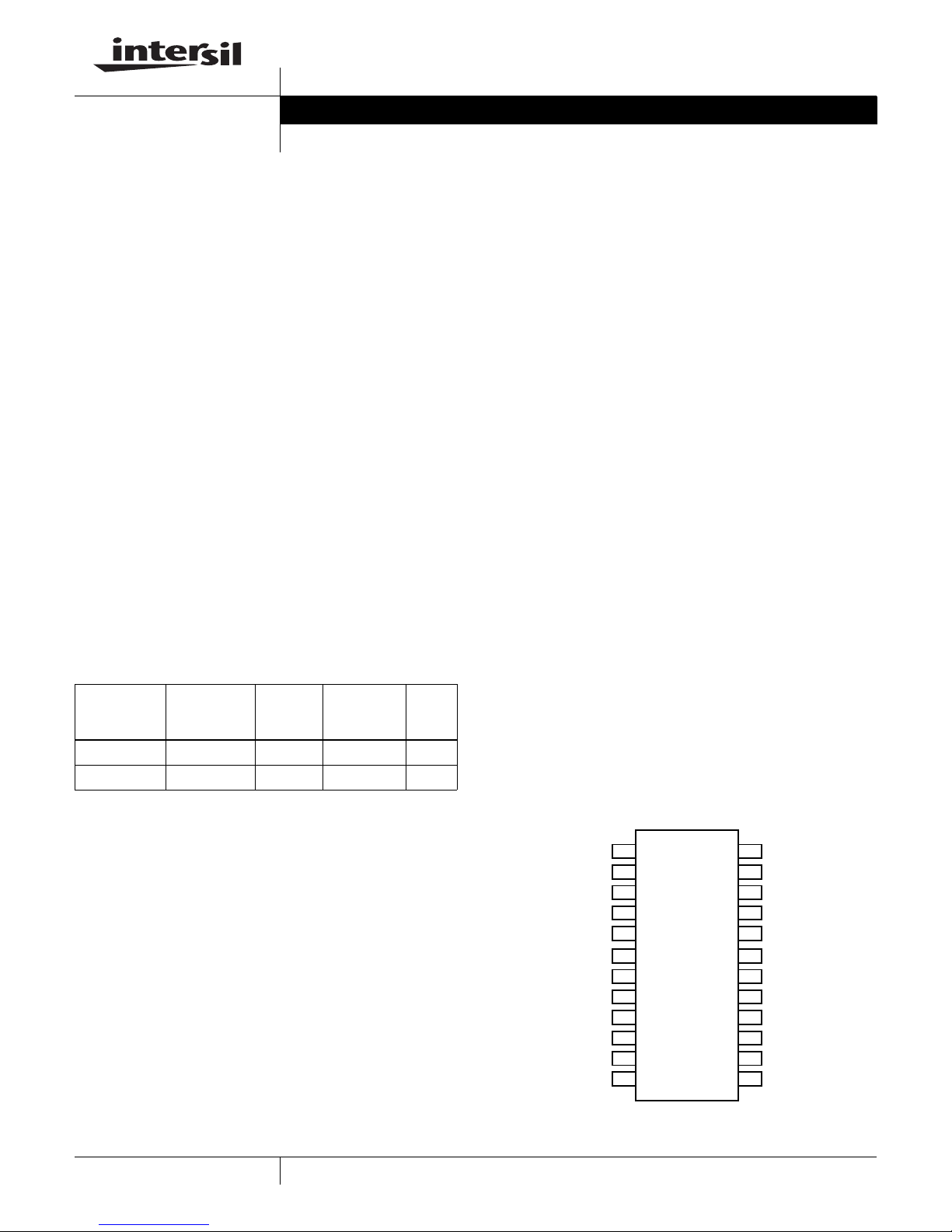
Pinout
ISL6252, ISL6252A
(24 LD QSOP)
TOP VIEW
VDD
EN
CELLS
ICOMP
VCOMP
ICM
VREF
CHLIM
ACLIM
VADJ LGATE
GND PGND
124
223
322
421
520
619
718
817
916
10 15
11 14
12 13
DCIN
ACPRN ACSET
CSON
CSOP
CSIN
CSIP
PHASE
UGATE
BOOT
VDDP
1
CAUTION: These devices are sensitive to electrostatic discharge; follow proper IC Handling Procedures.
1-888-INTERSIL or 1-888-468-3774
| Intersil (and design) is a registered trademark of Intersil Americas Inc.
All other trademarks mentioned are the property of their respective owners.
Copyright Intersil Americas Inc. 2007. All Rights Reserved
Page 2
Application Note 1362
What’s Inside
This Evaluation Board Kit contains the following materials:
• Qty(1) ISL6251EVAL2Z Evaluation Board
• Qty(1) ISL6252EVAL2Z Setup Procedure
What is Needed
The following materials are recommended to perform
testing:
• One adjustable 25V 6A power supply
• Two adjustable electronic loads with constant current
mode and constant voltage mode
• Two DVMs
• One 500MHz four channel oscilloscope
• Four passive oscilloscope voltage probes
• Two 10ADC Current Probes
• One signal generator
Jumper Selection Guide
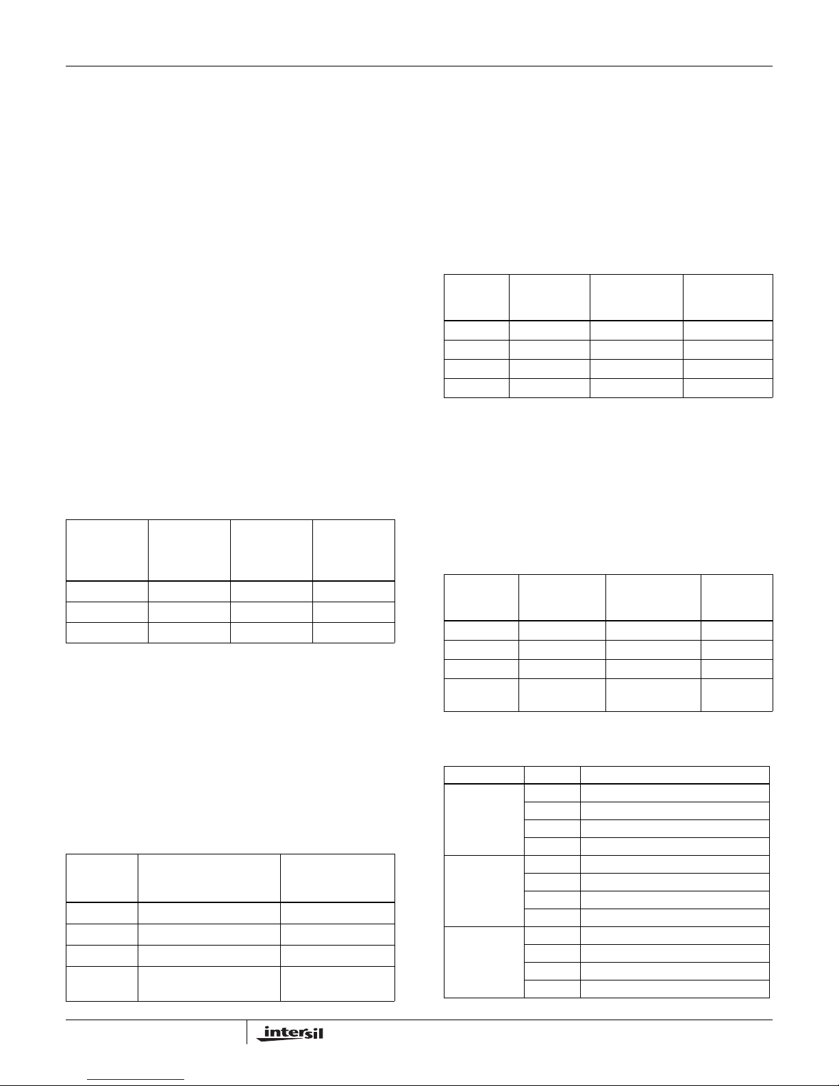
Step 1: Select the Number of Cells (Table 1)
The CELLS pin chooses the correct output voltage clamp for
a given number of cells series-connected in the battery pack.
Select the output voltage by placing a shunt jumper across
the appropriate pins of JP1.
TABLE 1. JUMPER JP1 FUNCTIONS
NUMBER OF
SHUNT
JUMPER
LOCATION
1-2 VDD 4 16.8
2-3 GND 3 12.6
Removed Floating 2 8.4
CELLS PIN
CONNECTED
TO:
CELLS
CONNECTED
IN SERIES
Step 2: Select the Cell Trim Voltage (Table 2)
The VADJ pin trims the battery charger output voltage limi t.
Preset battery charger output voltage limits are selected by
placing a shunt jumper across the appropriate pins of JP6.
For other battery charger output voltage limits install a shunt
jumper across pins 3 and 4 which connects the wiper of
potentiometer R24 to VADJ. Potentiometer R24 may be
removed and replaced with resistors R
R
limits the trim increase to 1%. Shorti ng R20 allows the
20
trim to increase 5%. Decreasing trim range is unaffected.
TABLE 2. JUMPER JP6 FUNCTIONS
SHUNT
JUMPER
LOCATION
1-3 Through R
3-5 To GND -5%
5-6 Floating None
3-4 R24 Wiper or R
VADJ
PIN
to VREF +5%
20
19/R21
and R21. Resistor
19
BATTER Y VOLTAG E
CHANGE PER CELL
Adjustable between
100%
CONSTANT
OUTPUT
VOLTAGE
-5% to +5%
Step 3: Select the Battery Charger Current Limit
(Table 3)
The CHLIM pin chooses the desired battery charger current
limit threshold. Preset battery charger current limit
thresholds are selected by placing a shunt jumper across the
appropriate pins of JP4. For other battery charger current
limit thresholds, install a shunt jumper across pins 3 and 4,
which connects the wiper of potentiometer R22 to CHLIM.
Potentiometer R22 may be removed and replaced with
resistors R
SHUNT
JUMPER
LOCATION
Removed Floating 0V 0A
and R7.
6
TABLE 3. JUMPER JP4 FUNCTIONS
CHLIM PIN
CONNECTED
TO:
1-3 VREF 120mV 4.80A
3-5 GND 0V 0A
3-4 R22 or R
100% CURRENT
FEEDBACK
CSOP TO CSON
0mV to 120mV 0A to 4.8A
6/R7
100%
CONSTANT
CURRENT
Step 4: Select the AC Adapter Current Limit (Table 4)
The ACLIM pin chooses the desired AC adapter current limit
threshold. Preset AC adapter current limit thresholds are
selected by placing a shunt jumper across the appropriate
pins of JP5. For other AC adapter current limit thresholds,
install a shunt jumper across pins 3 and 4 which con nect s the
wiper of potentiometer R23 to ACLIM. Potentiometer R23
may be removed and replaced with resistors R
TABLE 4. JUMPER JP5 FUNCTIONS
SHUNT
JUMPER
LOCATION
1-3 VREF 100mV 5.15A
Removed Floating 75mV 3.90A
3-5 GND 50mV 2.65A
3-4 R23 or R
ACLIM PIN
CONNECTED
TO:
17/R18
100% CURRENT
FEEDBACK
CSIP TO CSIN
50mV to 100mV 2.65A to
and R18.
17
ADAPTER
CURRENT
100%
5.15A
Interface Connections
TABLE 5.
HEADER PIN# CONNECT TO
H1
Input Power
H2
System Load
Output
H3
Battery Charger
Output
1 “+” INPUT POWER
2 “+” SENSE (if used)
3 “-” SENSE (if used)
4 “-” INPUT POWER
1 “+” SYSTEM LOAD OUTPUT
2 “+” SENSE (if used)
3 “-” SENSE (if used)
4 “-” SYSTEM LOAD OUTPUT
1 “+” BATTERY CHARGER OUTPUT
2 “+” SENSE (if used)
3 “-” SENSE (if used)
4 “-” BATTERY CHARGER OUTPUT
2
AN1362.0
October 25, 2007
Page 3
3
AN1362.0
October 25, 2007
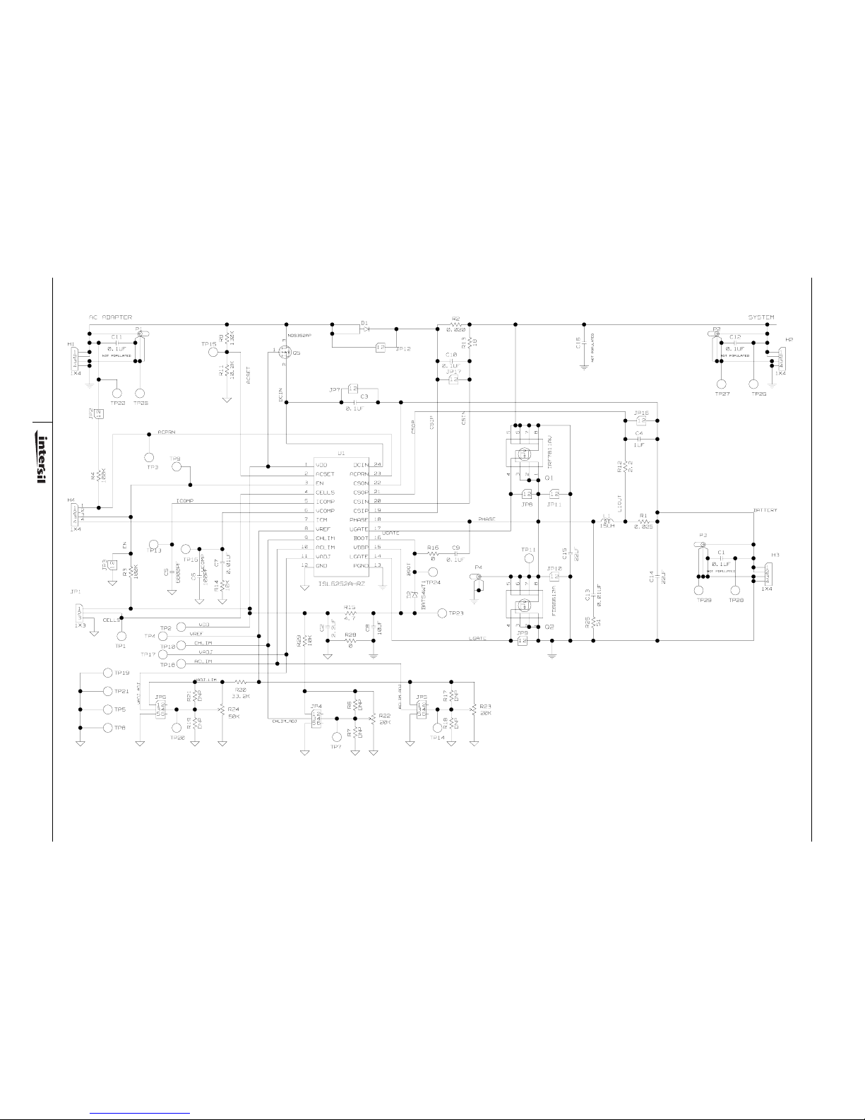
ISL6252AEVAL2Z Schematic
2
4
6
538
1
7
3
4
1
2
C2
TP19
VADJ_ADJ
R19
DNP
33.2K
R20
50K
L1OUT
0.1UF
LGATE
130K
AC ADAPTER
0.1UF
100K
100K
20K
100PF
VCOMP
ACPRN
FDS6612A
BAT54WT1
NOT POPULATED
ISL6252AHRZ
0.01UF
DNP
NOT POPULATED
VREF
NDS352AP
DNP
CELLS
EN
6800PF
CHLIM
VADJ_LIM
ACLIM
DNP
VADJ
10.2K
DCIN
ACSET
CHLIM_ADJ
0
20K
DNP
BOOT
0
0.1UF
CSOP
CSIP
CSIN
PHASE
0.01UF
22UF
22UF
15UH
0.025
2.2
1UF
0.1UF
NOT POPULATED
BATTERY
NOT POPULATED
SYSTEM
UGATE
4.7
0.1UF
VDD
ICOMP
10UF
ACLIM_ADJ
10K
2.2UF
10K
51
IRF7811AV
0.1UF
0.020
18
DNP
H2
TP26
C12
P2
TP27
H3
P3
TP28
C1
TP29
JP16
C4
R12
C16
JP11JP8
C14
R1
L1
C15
C13
JP10
TP11
R25
JP9
Q1
567
8
4
1
2
3
Q2
R2
R13
C10
JP17
JP12
D1
C3
JP7
P4
C9
R16
TP24
TP23
D2
C8
R15
Q5
3
1
2
R8R11
TP15
P1
TP25
TP3
TP9
TP16
C7
R14
C6
TP13
C5
TP2
TP10
TP4
TP17
TP18
C11
TP22
JP2
H1
R4
R3
JP3
H4
TP1
TP21
JP1
R23
JP5
TP14
R22
TP7
JP4
R24
TP20
JP6
TP5
TP8
U1
1
10
11
12 13
14
15
16
17
18
19
2
20
21
22
23
24
3
4
5
6
7
8
9
R28
R29
R7
R21
R6
R17R18
1X4
2
1
3
4
6
4
2
1
5
3
1
2
1X4
2
1
3
4
1X3
1
2
3
6
4
2
1
5
3
6
4
2
1
5
3
EN
DCINVDD
CELLS
ICOMP
VCOMP
VREF
ICM
ACSET
CHLIM
ACLIM
VADJ
GND PGND
LGATE
VDDP
BOOT
UGATE
PHASE
CSIP
CSIN
CSOP
CSON
ACPRN
1
2
1
2
1
2
1
2
1
2
1
2
1
2
1X4
2
1
3
4
1
2
1X4
2
1
3
4
1
2
Application Note 1362
Page 4
Application Note 1362
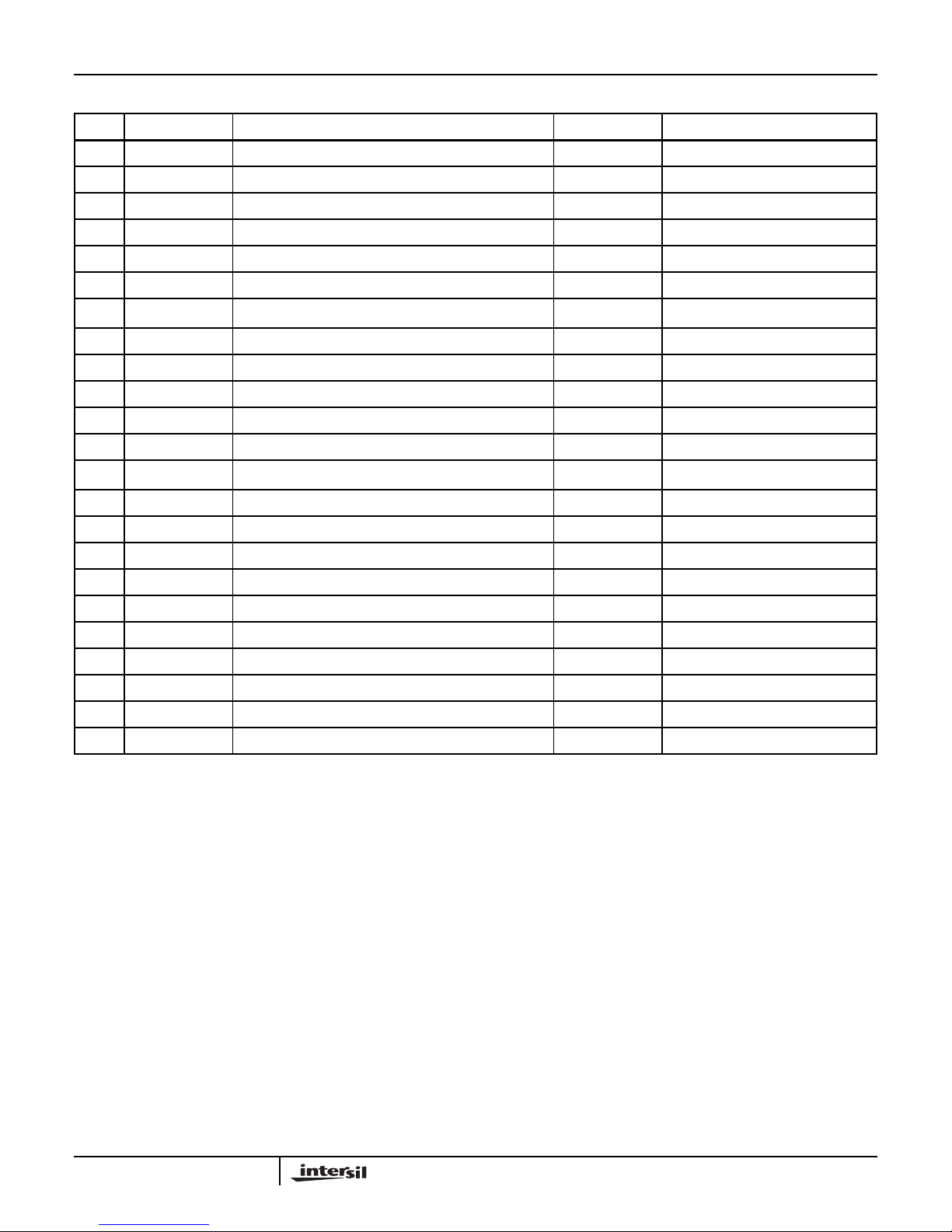
TABLE 6. BILL OF MATERIALS
QTY REF DES DESCRIPTION MFG NAME PART NUMBER
1 C6 Capacitor, SMD, 0603, 100pF, 50V, 5%, COG TDK C1608COG1H101J
1 C7 Capacitor, SMD, 0805, 0.01µF, 50V, 5%, COG TDK C2012COG1H103J
1 C5 Capacitor, SMD, 0805, 6800pF, 50V, 5%, COG TDK C2012COG1H682J
3 C2, C4, C8 Capacitor, SMD, 0805, 1.0µF, 16V, 20%, X7R TDK C2012X7R1C105M
3 C3, C9, C10 Capacitor, SMD, 0805, 0.1µF, 50V, 10%, X7R TDK C2012X7R1H104K
2 C14, C15 Capacitor, SMD, 1812, 22µF, 25V, 20%, X5R TDK C4532X5R1E226M
1D2
1 L1 Choke, SMD, 8mm, 15µH, 20%, 5.65A, Shielded Sumida CDRH127/LD-150NC
1 U1 IC, Battery Charger, 24 Ld QSOP, -10°C to +100°C Intersil ISL6252HAZ
1 Q2 MOSFET, N-CH, 8P, SOIC, 30V, 8.4A, 0.022Ω Fairchild FDS6612A
1 Q1 MOSFET, N-CH, 8P, SOIC, 30V, 10.8A, 0.011Ω IR IRF7811AV
1 Q5 MOSFET, P-CH, 3P, SOT23, -30V, -0.9A, 0.5Ω Fairchild NDS352AP
SURFACE MOUNT SCHOTTKY BARRIER DIODE
Diodes Inc. BAT54WT1
1D1
1 R2 Resistor, Shunt, SMD, 2010, 0.020Ω, 1W, 1% IRC LRC-LRF2010-01-R020-F
1 R1 Resistor, Shunt, SMD, 2010, 0.025Ω, 1W, 1% IRC LRC-LRF2010-01-R025-F
1 R13 Resistor, SMD, 0805, 18Ω, 0.125W, 5% KOA RK73B2AT180J
1 R12 Resistor, SMD, 0805, 2.2Ω, 0.125W, 5% KOA RK73B2AT2R2J
1 R15 Resistor, SMD, 0805, 4.7Ω, 0.125W, 5% KOA RK73B2AT4R7J
1 R14 Resistor, SMD, 0805, 10kΩ, 0.125W, 1% KOA RK73H2AT1002F
1 R11 Resistor, SMD, 0805, 7.87kΩ, 0.125W, 1% KOA RK73H2AT7871F
3 R3, R4, R8 Resistor, SMD, 0805, 100kΩ, 0.125W, 1% KOA RK73H2AT1003F
1 R20 Resistor, SMD, 0805, 33.2kΩ, 0.125W, 1% KOA RK73H2AT3322F
1 R16 Resistor, SMD, 0805, 0Ω, 2A, 50mΩ Max KOA RK73Z2AT
DIODE SCHOTTKY 40V 10A POWERDI5
Diodes Inc. PDS1040-13
4
AN1362.0
October 25, 2007
Page 5
5
AN1362.0
October 25, 2007
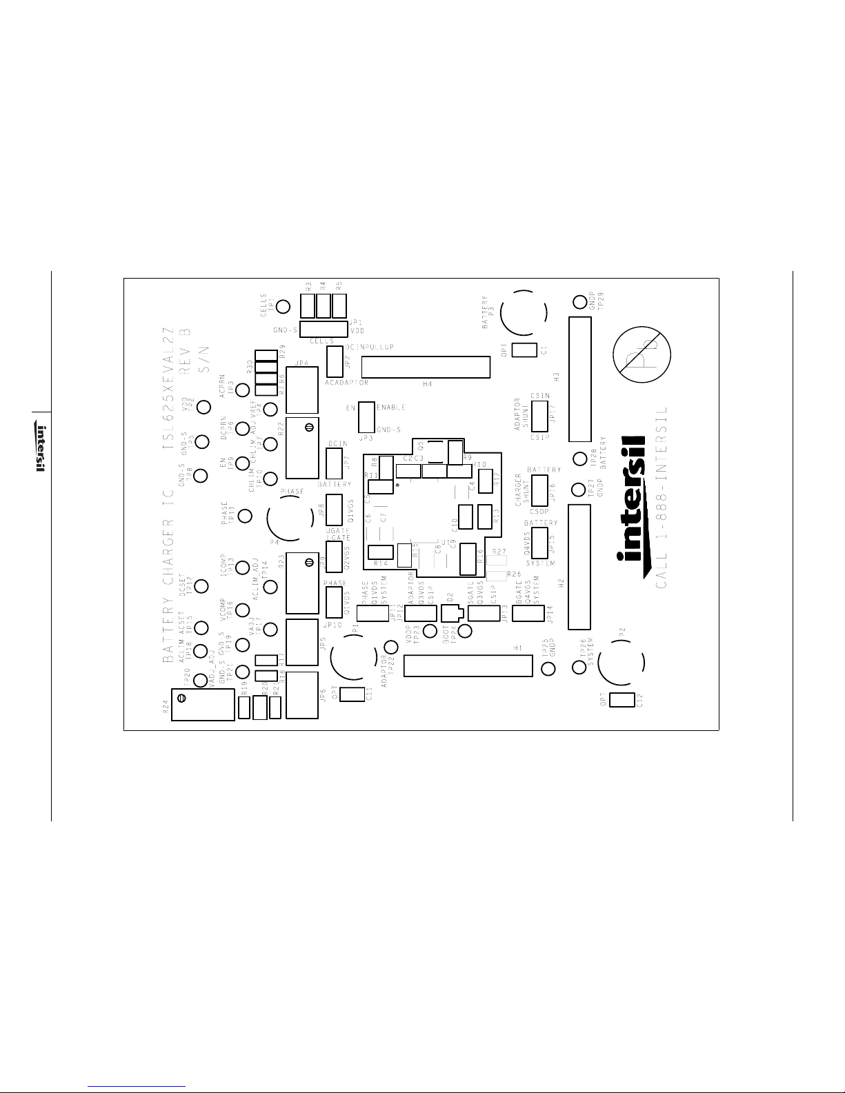
FIGURE 1. TOP SILK
Application Note 1362
Page 6
6
AN1362.0
October 25, 2007
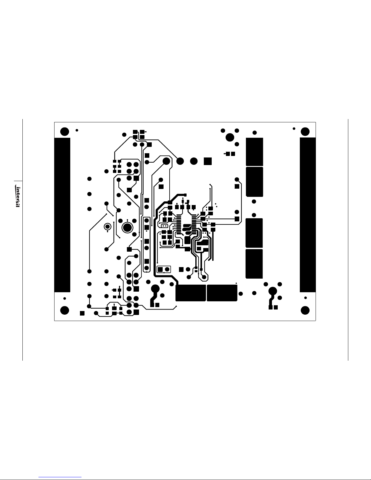
FIGURE 2. TOP LAYER
Application Note 1362
Page 7
7
AN1362.0
October 25, 2007
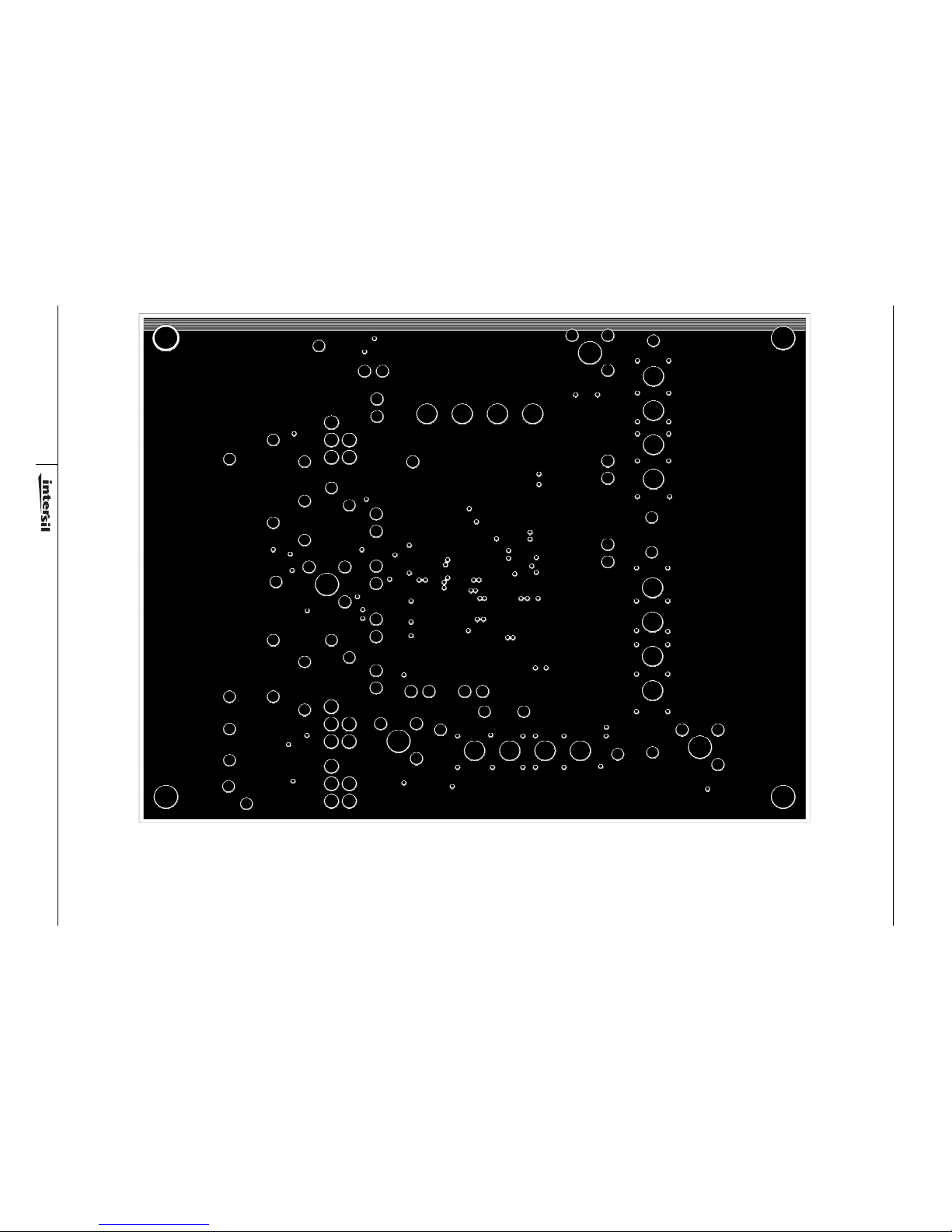
FIGURE 3. LAYER 2 GROUND (TOP VIEW)
Application Note 1362
Page 8
8
AN1362.0
October 25, 2007
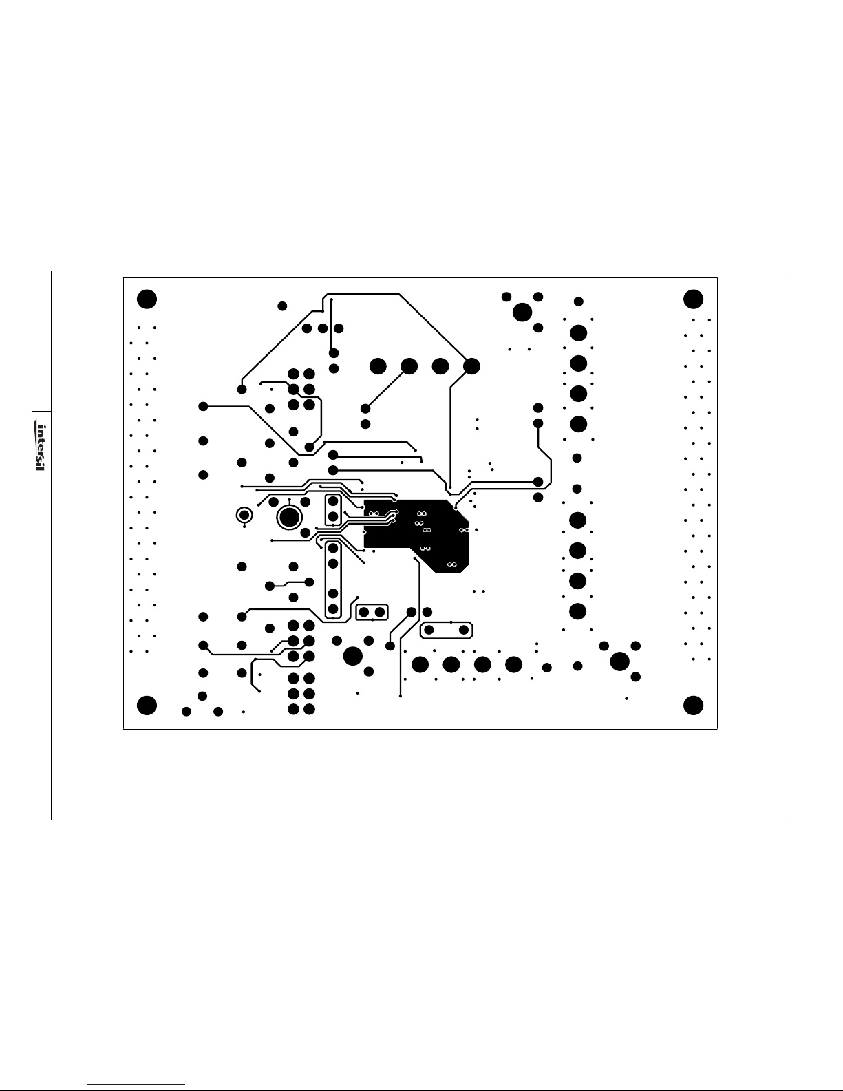
FIGURE 4. LAYER 3 SIGNAL (TOP VIEW)
Application Note 1362
Page 9
9
AN1362.0
October 25, 2007
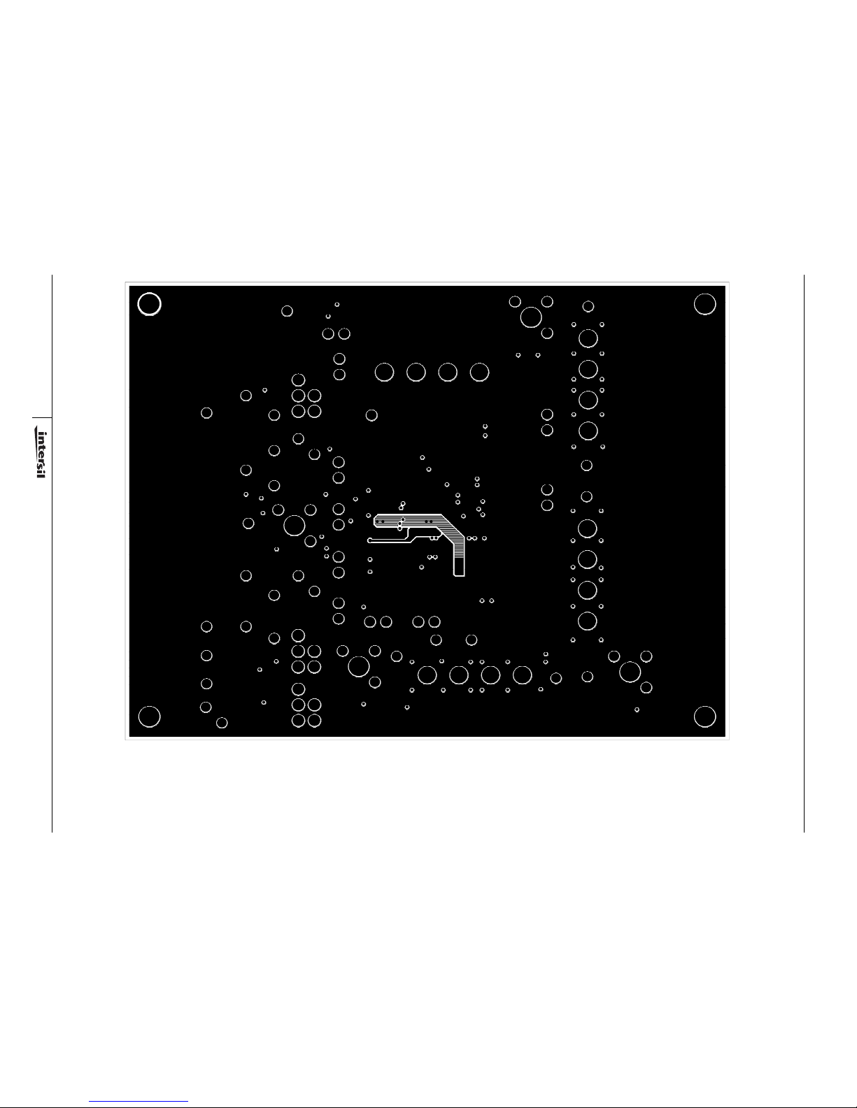
FIGURE 5. LAYER 4 GROUND (TOP VIEW)
Application Note 1362
Page 10
10
AN1362.0
October 25, 2007
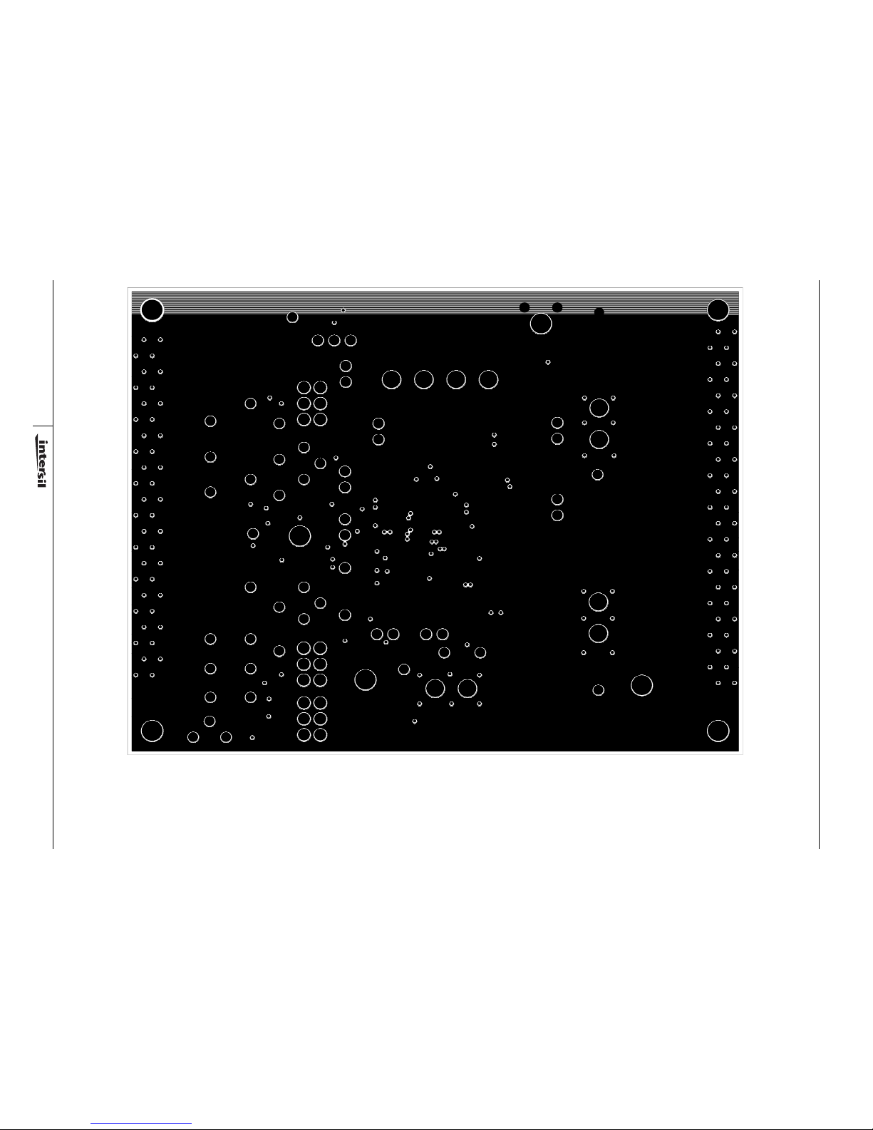
FIGURE 6. LAYER 5 GROUND (TOP VIEW)
Application Note 1362
Page 11
11
AN1362.0
October 25, 2007
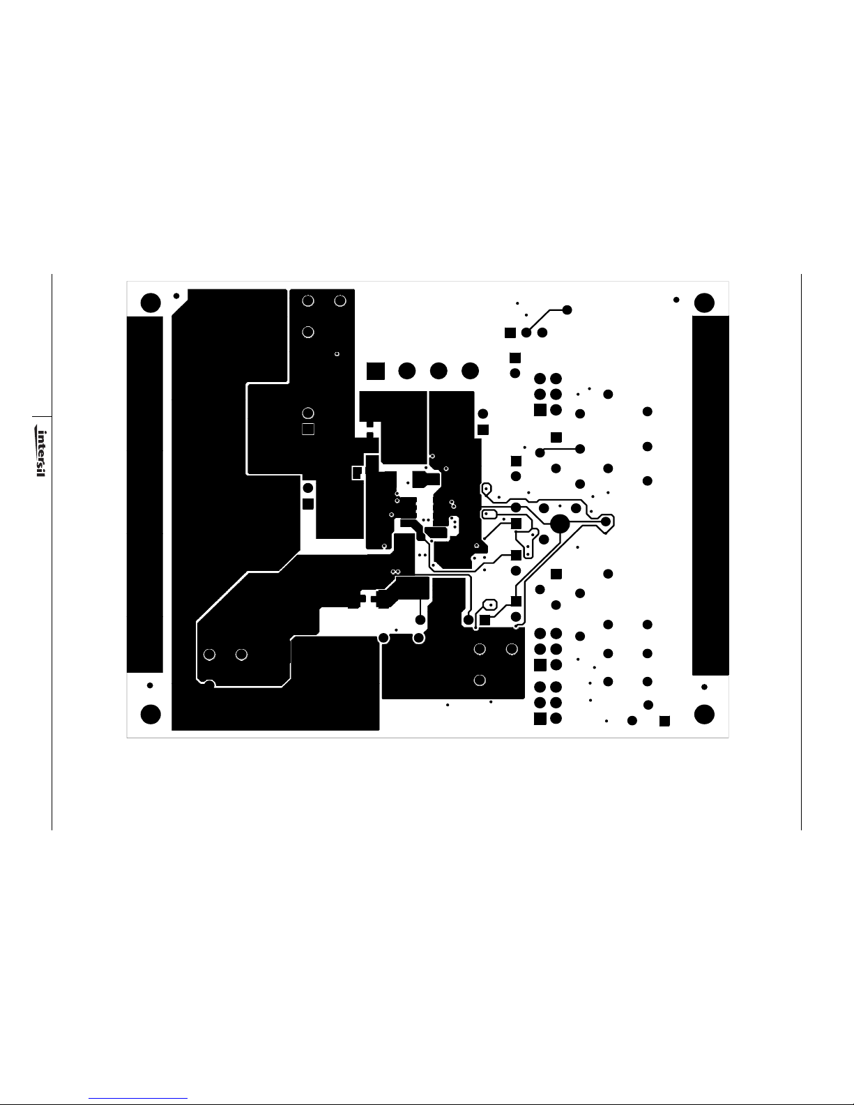
FIGURE 7. BOTTOM COPPER (BOTTOM VIEW)
Application Note 1362
Page 12
12
AN1362.0
October 25, 2007
Intersil Corporation reserves the right to make changes in circuit design, software and/or specifications at any time without notice. Accordingly, the reader is cautioned to verify that the Application Note or Technical Brief is
current before proceeding.
For information regarding Intersil Corporation and its products, see www.intersil.com
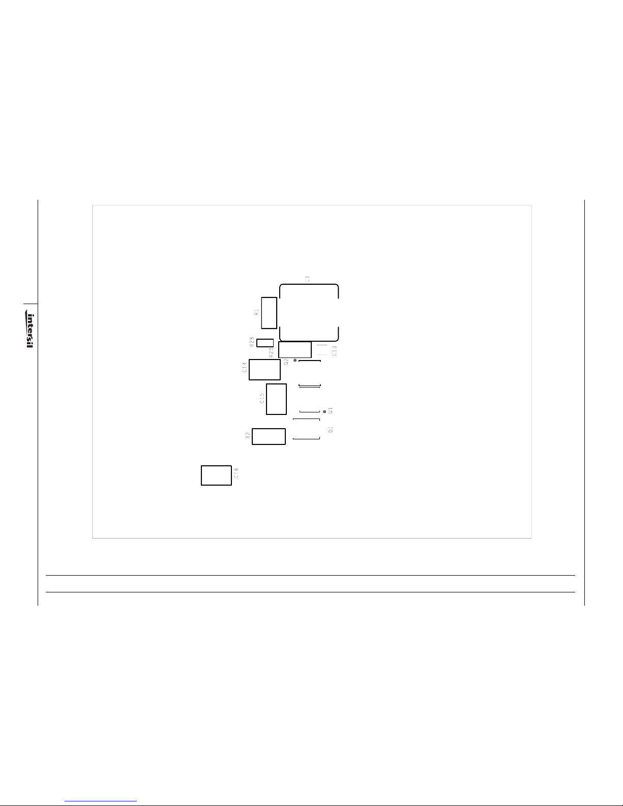
FIGURE 8. BOTTOM SILK SCREEN (BOTTOM VIEW)
Application Note 1362
 Loading...