

Page 1
®
ISL62381, ISL62382 Quad-Output Evaluation
Board User Guide
July 31, 2008 AN1396.0Application Note
Introduction
The ISL62381 and ISL62382 evaluation boards demonstrate
the performance of ISL62381 and ISL62382 Quad-output
controllers. The ISL62381 and ISL62382 controller include
two pulse-width modulation (PWM) controllers featured with
Intersil’s patented R
3
technology, adjustable from 0.6V to
5.5V, and two linear regulators, LDO5 and LDO3, that
generate a fixed 5V and an adjustable output respectively.
The evaluation board includes two independent Enable
switches, two LED Power-Good indicators and various test
points. Included with each switching channel is an on-board
dynamic load generator for evaluating the transient-load
response. There are four different evaluation boards which
provide flexible evaluation options. Table 1 shows a brief
description of the evaluation boards.
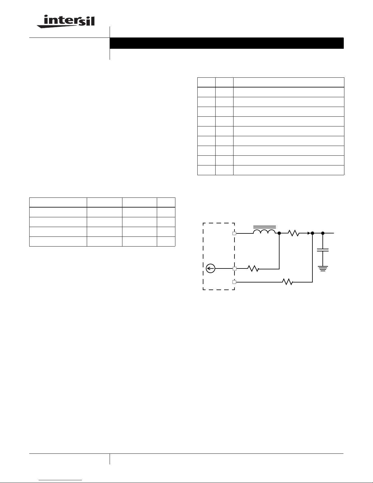
TABLE 1. EVALUATION BOARD DESCRIPTION
EVALUATION BOARD CHANNEL-1 CHANNEL-2 OCP
ISL62381LOEVAL1Z 3.3V/8A 5V/8A ~10A
ISL62381HIEVAL1Z 1.05V/15A 1.5V/15A ~20A
ISL62382LOEVAL1Z 3.3V/8A 5V/8A ~10A
ISL62382HIEVAL1Z 1.05V/15A 1.5V/15A ~20A
What’s Inside
The Evaluation Board Kit contains the following materials:
• ISL6238xxxEVAL1Z Evaluation Board
• ISL62381 and ISL62382 Datasheet
• ISL62381 And ISL62382 Evaluation Board User Guide
(this document)
What’s Needed
The following materials will be needed to perform testing:
• Adjustable +25V, 30A Power Supply
• +12V, 100mA Power Supply
• Precision digital multi-meter
• 4 Electronic Loads
• 4-Channel Oscilloscope
Enable Control
The evaluation board provides flexible control logic to enable
or disable the outputs, and to program the two PWM
channels’ start-up sequence. For start-up timing sequence,
please refer to the datasheet waveforms. Table 2 is the
Enable controller truth table.
.
EN1 EN2 START-UP SEQUENCE
Low Low Both Channel outputs OFF simultaneously
Low Float Both Channel outputs OFF simultaneously
Float Low Both Channel outputs OFF simultaneously
Float Float Both Channel outputs OFF simultaneously
Low High Channel-1 OFF, Channel-2 ON
High Low Channel-1 ON, Channel-2 OFF
High High Both Channel outputs ON simultaneously
Float High Channel-1 enabled after Channel-2 is in regulation
High Float Channel-2 enabled after Channel-1 is in regulation
TABLE 2. ENABLE TRUTH TABLE
Resistor Current Sense Configuration
The evaluation board is pre-configured with inductor DCR
current sense. For more precise overcurrent protection, it
also provides the option of resistor current sense. Figure 1
shows the configuration for resistor current sense.
L
PHASEx
ISL62381
ISL62382
10µA
OCSETx
ISENx
FIGURE 1. RESISTOR CURRENT SENSE CIRCUIT
R
_
V
ROCSET
OCSET
+
For Channel - 1, t h e ISL62381 and ISL62382 monitors th e
OCSET1 pin and the ISEN1 pin voltages. Once the OCSET1
pin voltage is higher than the ISEN1 pin voltage for more than
10µs, the ISL62381 and ISL62382 declare an overcurrent
fault. For a chosen overcurrent, set point I
sense resistor R
SENSE
, the value of R
by Equation 1
IOCR
•
SENSE
R
OCSET
-------------------------------------
=
10μ A
Where:
-R
(Ω) is the resistor used to program the
OCSET
overcurrent setpoint
is the output current threshold that will activate the
-I
OC
OCP circuit
-R
R
is current sense resistor (R3 for Channel-1 and
SENSE
for Channel-2)
25
R
SENSE
+
V
RSENSE
R
O
OCSET
I
L
_
and current
OC
is determined
V
O
C
O
(EQ. 1)
1
CAUTION: These devices are sensitive to electrostatic discharge; follow proper IC Handling Procedures.
1-888-INTERSIL or 1-888-468-3774
| Intersil (and design) is a registered trademark of Intersil Americas Inc.
All other trademarks mentioned are the property of their respective owners.
Copyright Intersil Americas Inc. 2008. All Rights Reserved
Page 2
Application Note 1396
Take Channel-1 as an example, once the value of R
OCSET
is calculated, follow the following procedure to configure the
resistor current sense circuit:
Step 1: Open the “DCR SENSE” sold er bridge and
connect the “RESISTOR SENSE” solder bridge
on the PCB bottom layer;
Step 2: Remove R7 (R22 for Channel 2);
Step 3: Replace R
Step 4: Replace C
(R25 for Channel 2) with R
3
(C25 for Channel 2) with R
6
SENSE
OCSET;
;
Dynamic Load Generator
The evaluation board provides each PWM channel an
on-board dynamic load generator for evaluating the
transient-load response, which are controlled by SW1 and
SW2 respectively. The dynamic load generator applies a
300µs pulse load across V
slew-rate can be trimmed by adjusting the resistors R
for the rising edge, and R
power supply is needed to power the dynamic load
generator.
and GND. The transient load
OUT
, R39 for the falling edge. +12V
38
Step 5: Replace replace R19 (R18 for Channel 2) with
R
OCSET.
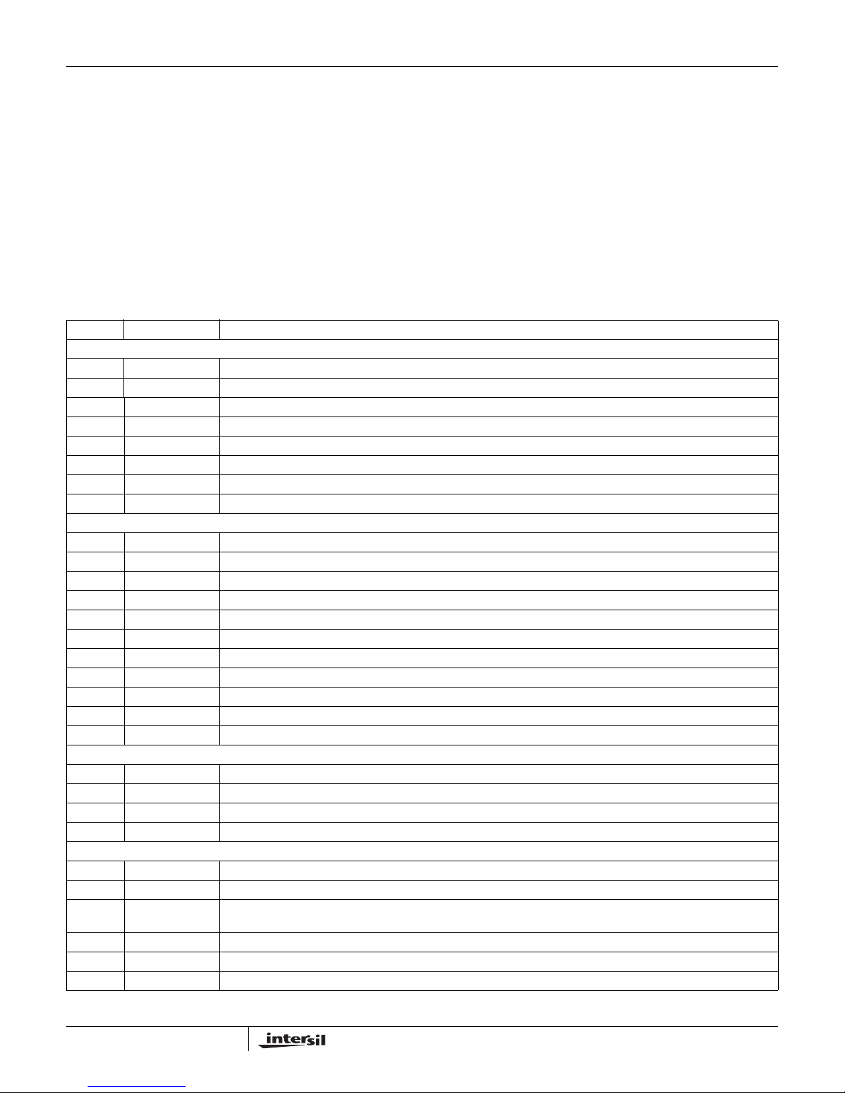
Connections and Test Points The following table describes the function and operation of the evaluation boards.
NUMBER NAME FUNCTION/OPERATION
INTERFACES AND CONNECTIONS
TP3 VBAT V
TP4 GND V
TP1 VOUT1 Channel-1 positive power output
TP2 GND Channel-1 return power output
TP11 VOUT2 Channel-2 positive power output
TP12 GND Channel-2 return power output
TP20 +12V +12V positive power input, used for the power supply of the on-board dynamic-load generator
TP19 GND +12V return power input
TEST POINTS
J1 PHASE2 Scope-probe socket for measuring Channel-2 phase node
J3 PHASE1 Scope-probe socket for measuring Channel-1 phase node
J2 VOUT1 Scope-probe socket for measuring Channel-1 output
J5 VOUT2 Scope-probe socket for measuring Channel-2 output
J4 FLOAT_FCCM Remove the jumper will float the FCCM pin
J6 FLOAT_EN1 Remove the jumper will float the EN1 pin
J7 FLOAT_EN2 Remove the jumper will float the EN2 pin
TP17 EN1 Test point of EN1 pin
TP8 EN2 Test point of EN2 pin
TP9 LDO3EN Test point of LDO3EN pin
TP10 FCCM Test point of FCCM pin
POWER-GOOD INDICATORS
TP13 PGOOD1 Test point of PGOOD1 pin
TP5 PGOOD2 Test point of PGOOD2 pin
D1 Channel-1 Power-Good indicator. Green when VOUT1 is in regulation.
D2 Channel-2 Power-Good indicator. Green when VOUT2 is in regulation.
LINEAR REGULATORS
TP14 LDO5 LDO5 linear regulator positive power output
TP15 GND LDO5 linear regulator return power output
TP16 LDO3IN Input of LDO3 linear regulator. Connect to connected to a voltage greater than the LDO3 set point plus the dropout
TP18 LDO3FB LDO3 linear regulator output voltage feedback test point
TP6 LDO3 LDO3 linear regulator positive power output
TP7 GND LDO3 linear regulator return power output
positive power input
IN
return power input
IN
voltage.
34
, R40
2
AN1396.0
July 31, 2008
Page 3
Application Note 1396
Connections and Test Points The following table describes the function and operation of the evaluation boards. (Continued)
SWITCHES
SW1 ON/OFF control of Channel-2 dynamic-load generator. Toggle to ON will enable the dynamic load, toggle to OFF
SW2 ON/OFF control of Channel-1 dynamic-load generator. Toggle to ON will enable the dynamic load, toggle OFF will
U2 ON: High level for EN1, EN2, LDO3EN and FCCM, respectively
will disable the transient load
disable the transient load
OFF: Low level for EN1, EN2, LDO3EN and FCCM, respectively
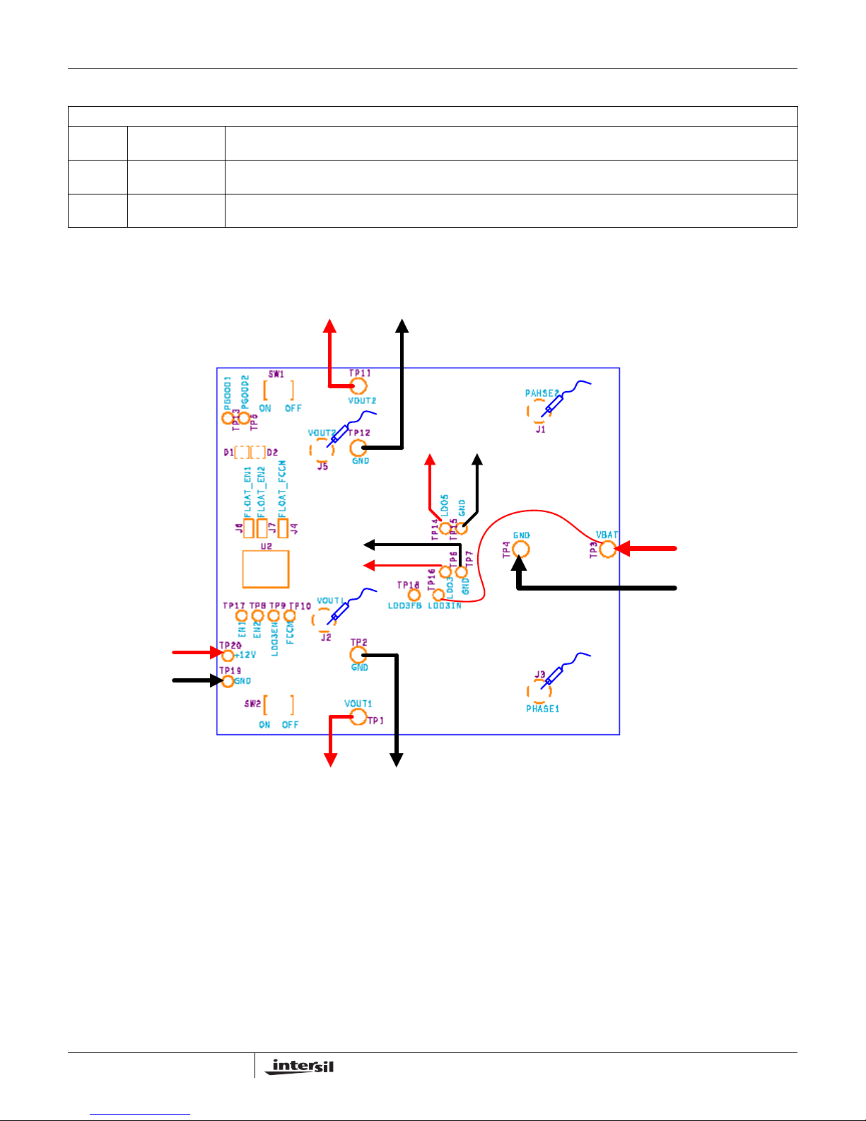
Test Set-up
Figure 2 shows a typical test configuration.
VOUT2
+
(0.6V~5.5V)
-
5V
+
-
+
12V
-
-
LDO3
(0.6V~5.5V)
+
VOUT1
+
(0.6V~5.5V)
FIGURE 2. TYPICAL TEST CONFIGURATION
-
+
VIN
(5.5V~25V)
-
PROBE
3
AN1396.0
July 31, 2008
Page 4
Application Note 1396
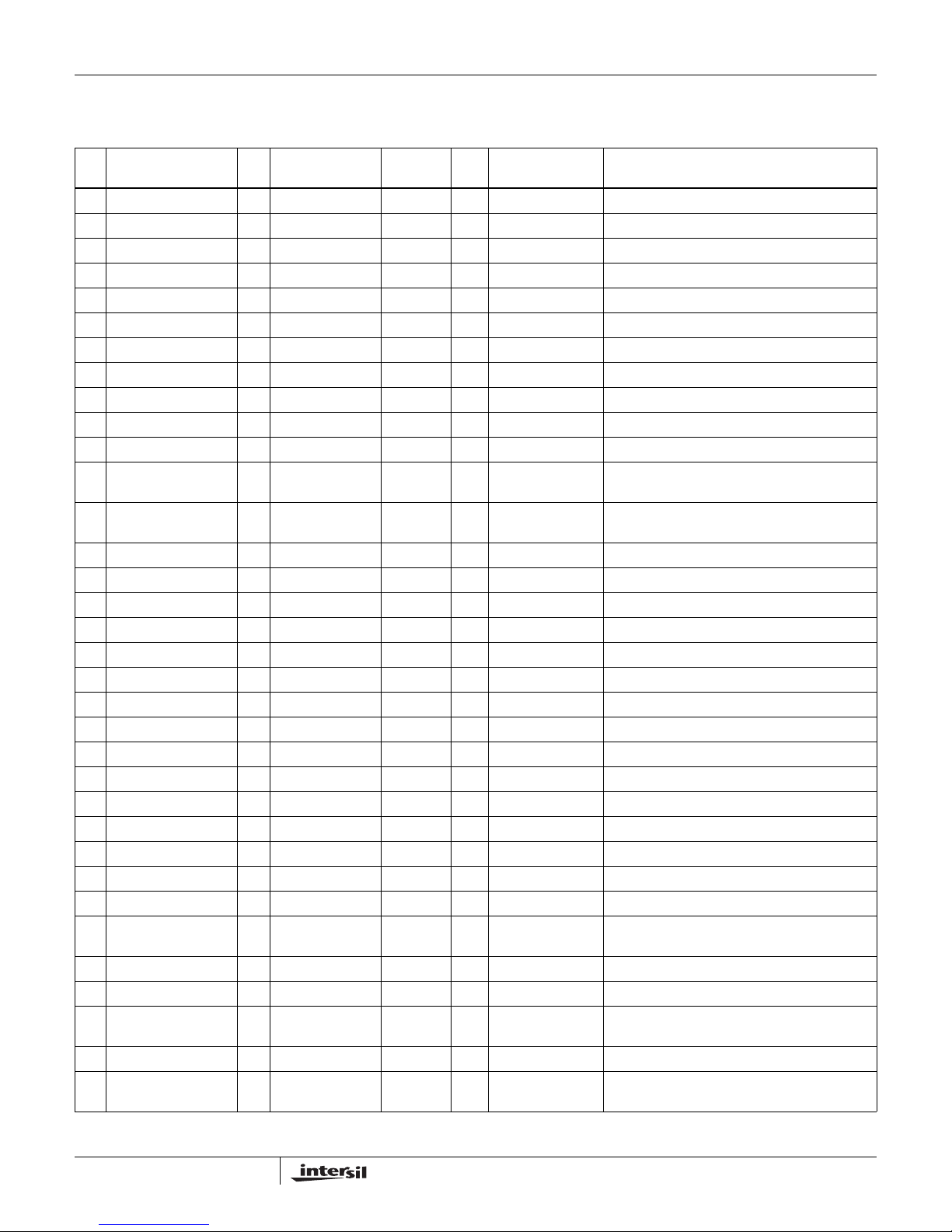
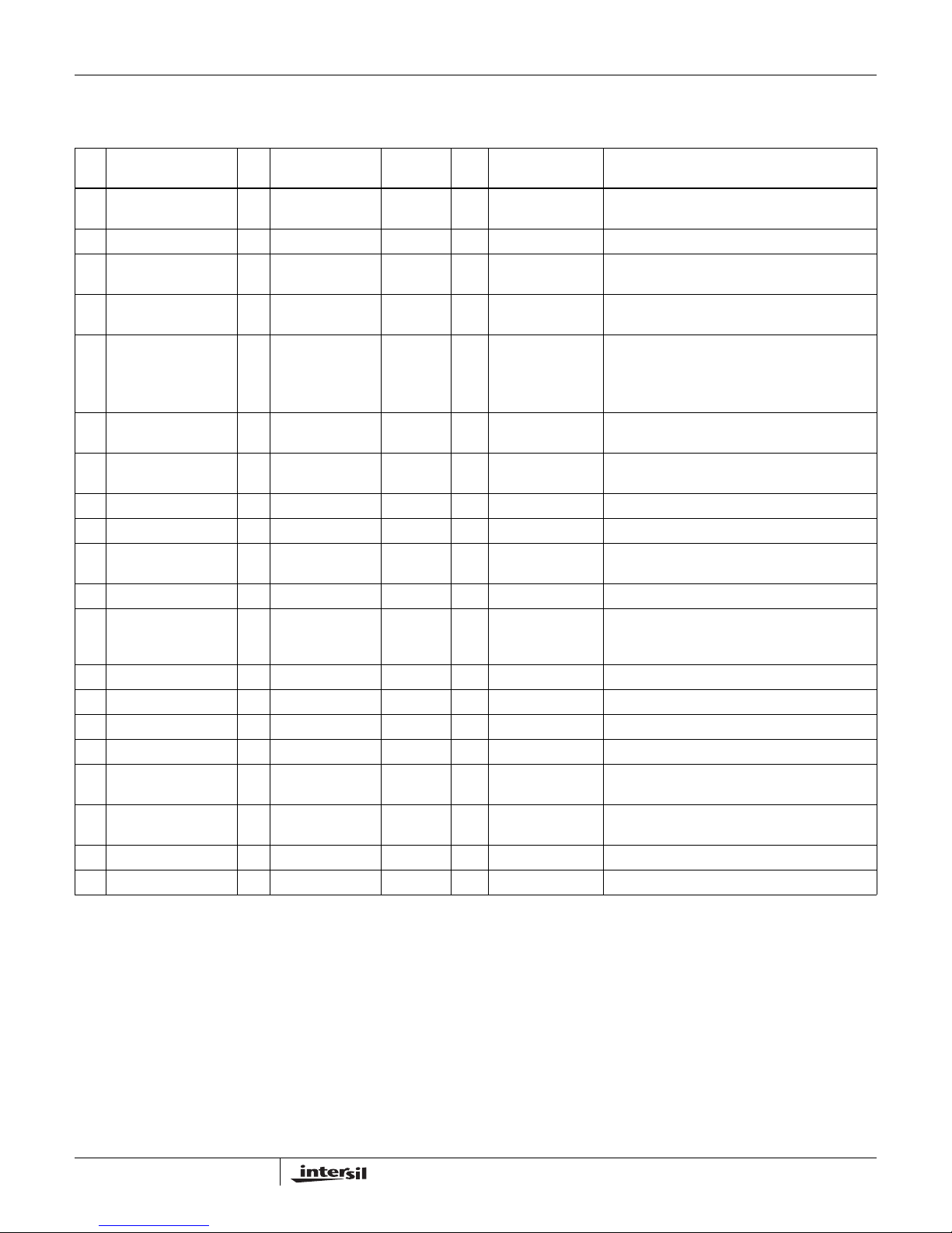
ISL62381LOEVAL1Z, ISL62382LOEVAL1Z Evaluation Board Bill of Materials
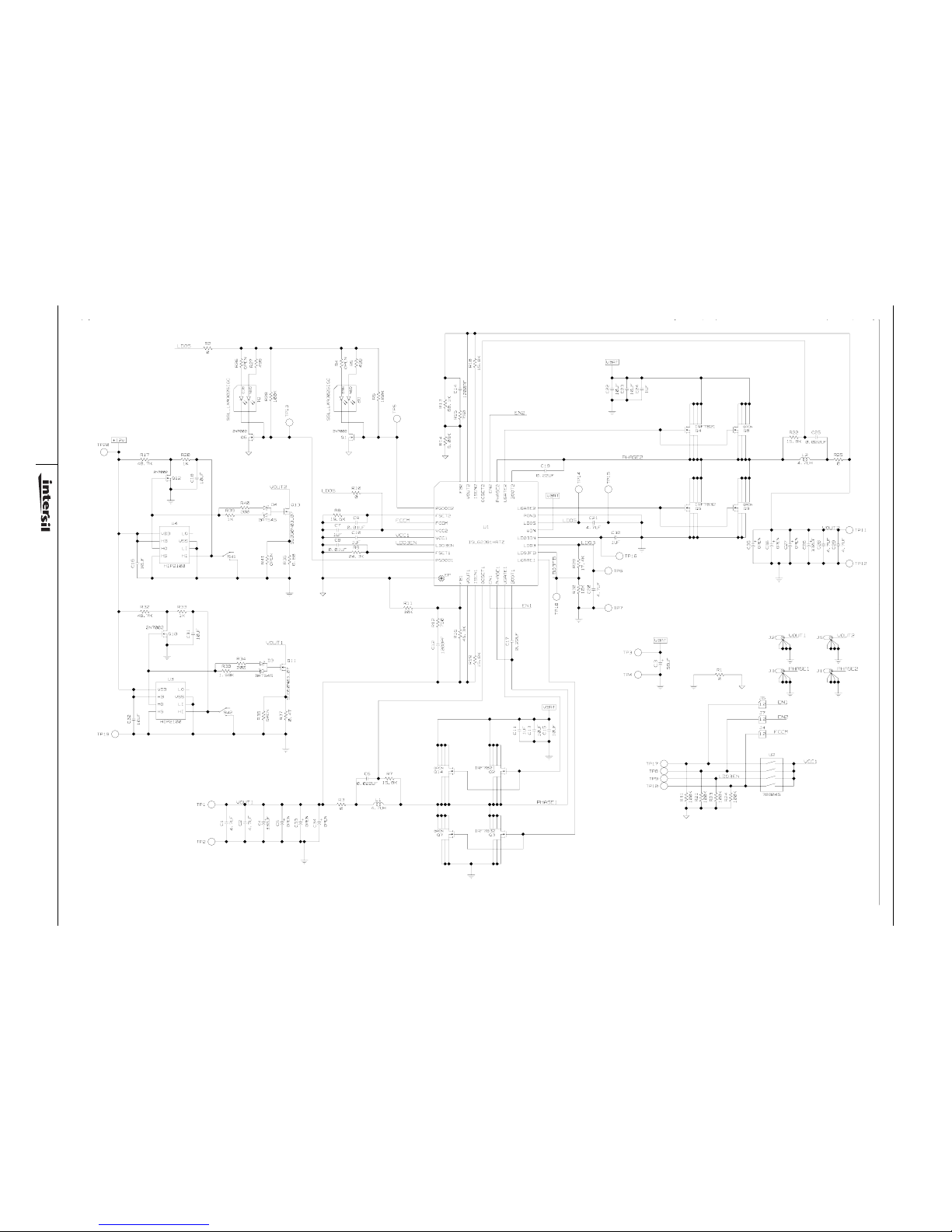
ISL62381LOEVAL1Z and ISL62382LOEVAL1Z evaluation boards use the same PCB and schematic, thus the same bill of materials except for the
controller U1.
REFERENCE
NO.
DESIGNATOR QTY VALUE
1 C6, C25 2 0.022µF 25V 10 GENERIC SM_CAP_0603, 0.022µF , 25V, 10%, X7R, ROHS
2 C8, C9 2 0.01µF 16V 10 GENERIC SM_CAP_0603, 0.01µF, 16V, 10%, X7R, ROHS
3 C17, C19 2 0.22µF 16V 10 GENERIC SM_CAP_0603, 0.22µF, 16V, 10%, X7R, ROHS
4 C13, C15, C22, C23 4 10µF 25V 10 GENERIC SM_CAP_1206, 10µF, 25V, 10%, X7R, ROHS
5 C12, C14 2 1200pF 16V 10 GENERIC SM_CAP_0603, 1200PF, 16V, 10%, X7R, ROHS
6 C7, C10 2 1µF 10V 10 GENERIC SM_CAP_0603, 1µF, 10V, 10%, X7R, ROHS
7 C30 1 1µF 25V 10 GENERIC SM_CAP_0805, 1µF, 25V, 10%, X7R, ROHS
8 C11, C24 2 1µF 25V 10 GENERIC SM_CAP_1206, 1µF, 25V, 10%, X7R, ROHS
9 C1, C2, C28, C29 4 4.7µF 10V 10 GENERIC SM_CAP_0805, 4.7µF, 10V, 10%, X7R, ROHS
10 C20, C21 2 4.7µF 10V 10 GENERIC SM_CAP_1206, 4.7µF, 10V, 10%, X7R, ROHS
11 C16, C18, C31, C32 4 10µF 16V 10 GENERIC SM_CAP_0805, 10µF, 16V, 10%, X5R, ROHS
12 C3 1 56µF 25V 20 SANYO-OSCON RADIAL_POLCAP_RADIAL, 25SP56M, 56µF,
13 C4, C26 2 330µF 6.3V 10 SANYO-POSCAP SM_POLCAP_SMD, 6TPF330M9L, 330UF,
14 R12, R15 2 750 1/10W 1 GENERIC SM_RES_0603, 750, 1/10W, 1%, TF, ROHS
15 R11, R30 2 10k 1/10W 1 GENERIC SM_RES_0603, 10k, 1/10W, 1%, TF, ROHS
16 R14 1 9.09k 1/10W 1 GENERIC SM_RES_0603, 9.09k, 1/10W, 1%, TF, ROHS
17 R13 1 68.1k 1/10W 1 GENERIC SM_RES_0603, 68.1k, 1/10W, 1%, TF, ROHS
18 R7, R18, R19, R22 4 15.8k 1/10W 1 GENERIC SM_RES_0603, 15.8k, 1/10W, 1%, TF, ROHS
19 R29 1 17.4k 1/10W 1 GENERIC SM_RES_0603, 17.4k, 1/10W, 1%, TF, ROHS
20 R8 1 19.6k 1/10W 1 GENERIC SM_RES_0603, 19.6k, 1/10W, 1%, TF, ROHS
21 R9 1 24.3k 1/10W 1 GENERIC SM_RES_0603, 24.3k, 1/10W, 1%, TF, ROHS
22 R16 1 45.3k 1/10W 1 GENERIC SM_RES_0603, 45.3k, 1/10W, 1%, TF, ROHS
23 R20, R33, R39 3 1k 1/10W 1 GENERIC SM_RES_0603, 1k, 1/10W, 1%, TF, ROHS
24 R38 1 1.58k 1/10W 1 GENERIC SM_RES_0603, 1.58k, 1/10W, 1%, TF, ROHS
25 R17, R32 2 48.7k 1/10W 1 GENERIC SM_RES_0603, 48.7k, 1/10W, 1%, TF, ROHS
26 R1, R2, R10 3 0 1/10W 1 GENERIC SM_RES_0603, 0, 1/10W, 1%, TF, ROHS
27 R34, R40 2 200 1/10W 1 GENERIC SM_RES_0603, 200, 1/10W, 1%, TF, ROHS
28 R5, R27 2 499 1 / 10W 1 GENERIC SM_RES_0603, 499, 1/10W, 1%, TF, ROHS
29 R6, R21, R23, R24,
R28, R31
30 R35 1 0.7 1W 1 GENERIC SM_RES_2512, 0.7, 1W, 1%, TF, ROHS
31 R37 1 0.5 1W 1 GENERIC SM_RES_2512, 0.5, 1W, 1%, TF, ROHS
32 D1, D2 2 SSL_LXA3025IGC LUMEX SSL_LXA3025IGC_SMD-SSL-LXA3025IGC,
33 D3, D4 2 BAT54S DIODES SM_SCHOTTKY_BAT54S-BAT54S, SOT23
34 Q2, Q4 2 IRF7821PBF IR 30V 13.6A N-Channel HEXFET Power MOSFET
6 100k 1/10W 1 GENERIC SM_RES_0603, 100k, 1/10W, 1%, TF, ROHS
VOLTAGE/
POWER
TOL.
(%) MANUFACTURER DESCRIPTION
25V, 20%, CASE-CC
6.3V, 10%, CAP_7343
LED_3x2_5MM
(Pb-free)
4
AN1396.0
July 31, 2008
Page 5
Application Note 1396
ISL62381LOEVAL1Z, ISL62382LOEVAL1Z Evaluation Board Bill of Materials
ISL62381LOEVAL1Z and ISL62382LOEVAL1Z evaluation boards use the same PCB and schematic, thus the same bill of materials except for the
controller U1. (Continued)
REFERENCE
NO.
DESIGNATOR QTY VALUE
35 Q3, Q5 2 IRF7832PBF IR 30V 20A N-Channel HEXFET Power MOSFET
36 Q1, Q6, Q10, Q12 4 2N7002-7-F FAIRCHILD 2N7002_SOT23-2N7002-7-F,SOT23
37 Q11, Q13 2 SUD50N03-07 VISHAY SUD50N03_07_TO252-SUD50N03-07,
38 SW1, SW2 2 GT11MSCBE-T C&K GT11MSCKE_SMT-GT11MSCBE-T,
39 TP5, TP6, TP7, TP8,
TP9, TP10, TP13,
TP14, TP15, TP16,
TP17, TP18, TP19,
40 TP1, TP2, TP3, TP4,
TP11, TP12
41 J1, J2, J3, J5 4 131-5031-00 TEKTRONIX SCOPE_PROBE_5P_CONN-131-5031-00,
42 J4, J6, J7 3 68000-236 FCI CONN2_DIP2-68000-236, CONN2
43 U2 1 78B04S GRAYHILL DIP_SW4_SPST_DIP-78B04S, DIP8-SW4
44 U1 1 ISL62381HRTZ
45 U3, U4 2 HIP2100IBZ INTERSIL HIP2100_SOIC-HIP2100IBZ,SOIC8_150_50
46 L1, L2 2 4.7µH 20% VISHAY VISHAY_IHLP_5050CE_SMT-20%-IHLP-
47 R3, R25 2 Wire GENERIC Wire short
48 DCR SENSE 4 Wire GENERIC Wire short
49 Jumper Connector 3 SPC02SYAN SULLINS Connector Jumper for J4, J6, J7
50 1 PCB TBD ISL62381EVAL1ZREVA PCB
51 1 Label TBD LABEL, FOR SERIAL NUMBER AND BOM
52 C5, C27, C33, C34,
C35, C36
53 R4, R26, R36, R41 4 No-pop
54 Q7, Q8, Q9, Q14 4 No-pop
14 5002 KEYSTONE TEST_POINT_THOLE-5002,MTP500X
6 1514-2 KEYSTONE TEST_POINT_THOLE-1514-2,TP-150C100P
(ISL62382HRTZ)
6 No-pop
VOLTAGE/
POWER
TOL.
(%) MANUFACTURER DESCRIPTION
(Pb-FREE)
TO-252AA
GT13MSCKE
TEK131-5031-00
INTERSIL ISL62381HRTZ, 32 LD 5x5 TQFN
(ISL62382HRTZ, 32 LD 5x5 TQFN)
5050CE-01-4R7M, 4.7µH, 24A, 20%,
VISHAY_IHLP-5050CE
REV #
5
AN1396.0
July 31, 2008
Page 6
Application Note 1396
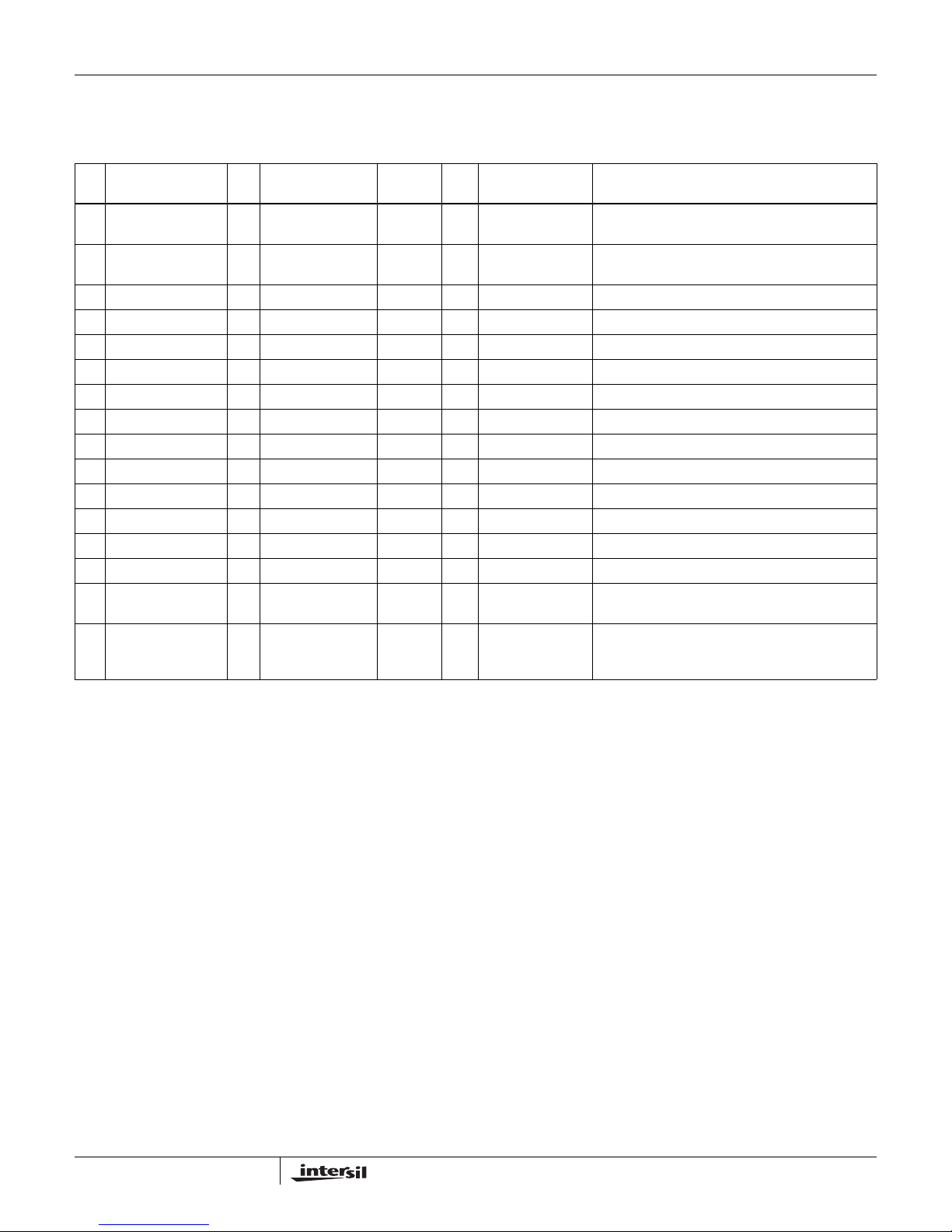
ISL62381HIEVAL1Z, ISL62382HIEVAL1Z Evaluation Board Bill of Materials
The ISL62381HIEVAL1Z, ISL62382HIEVAL1Z evaluation boards use the same PCB and schematic as the ISL62381LOEVAL1Z,
ISL62382LOEVAL1Z evaluation boards but dif ferent bill of materials (BOM). The following table shows the BOM dif ference of ISL62381HIEVAL1Z,
ISL62382HIEVAL1Z in comparison with ISL62381LOEVAL1Z, ISL62382LOEVAL1Z.
REFERENCE
NO.
DESIGNATOR QTY VALUE
1 Q8, Q14 2 IRF7821PBF IR 30V 13.6A N-Channel HEXFET Power MOSFET
2 Q7, Q9 2 IRF7832PBF IR 30V 20A N-Channel HEXFET Power MOSFET
3 R8 1 14k 1/10W 1 GENERIC SM_RES_0603, 14k, 1/10W, 1%, TF, ROHS
4 R9 1 17.4k 1/10W 1 GENERIC SM_RES_0603, 17.4k, 1/10W, 1%, TF, ROHS
5 R11 1 23.2k 1/10W 1 GENERIC SM_RES_0603, 23.2k, 1/10W, 1%, TF, ROHS
6 R16 1 17.8k 1/10W 1 GENERIC SM_RES_0603, 17.8k, 1/10W, 1%, TF, ROHS
7 R13 1 15k 1/10W 1 GENERIC SM_RES_0603, 15k, 1/10W, 1%, TF, ROHS
8 R14 1 10k 1/10W 1 GENERIC SM_RES_0603, 10k, 1/10W, 1%, TF, ROHS
9 R7, R18, R19, R22 4 16.2k 1/10W 1 GENERIC SM_RES_0603, 16.2k, 1/10W, 1%, TF, ROHS
10 R35 1 0.2 1W 1 GENERIC SM_RES_2512, 0.2, 1W, 1%, TF, ROHS
11 R37 1 0.1 1W 1 GENERIC SM_RES_2512, 0.1, 1W, 1%, TF, ROHS
12 R38 1 4.02k 1/10W 1 GENERIC SM_RES_0603, 4.02k, 1/10W, 1%, TF, ROHS
13 R12, R15 2 590 1/10W 1 GENERIC SM_RES_0603, 590, 1/10W, 1%, TF, ROHS
14 C12, C14 2 1800pF 16V 10 GENERIC SM_CAP_0603, 1800PF, 16V, 10%, X7R, ROHS
15 C33, C36 2 330µF 6.3V 10 SANYO-POSCAP SM_POLCAP_SMD, 6TPF330M9L, 330µF, 6.3V,
16 L1, L2 2 2.2µH 20 VISHAY VISHAY_IHLP_5050CE_SMT-20%-IHLP-5050CE-
VOLTAGE
/POWER
TOL.
(%) MANUFACTURER DESCRIPTION
(Pb-free)
(Pb-free)
10%, CAP_7343
01-2R2M,2.2µH, 29A, 20%, VISHAY_IHLP5050CE
6
AN1396.0
July 31, 2008
Page 7
7
AN1396.0
July 31, 2008
ISL6238xxxEVAL1Z Evaluation Board Schematic
ISL62381LOEVAL1Z
04/10/08
REV A
11
Q14
0.68
R35
OPEN
C35
L2
4.7UH
1200PF
R13
C14
1200PF
VOUT1
SUD50N03_07
Q11
Q13
SUD50N03_07
2N7002
IRF7821
Q4
IRF7832
IRF7821
10UF
1UF
R34
200
SW1
BAT54S
SSL_LXA3025IGC
2N7002
Q6
ISL62381HRTZ
R9
OPEN
C36
OPEN
R23
TP16
R38
TP5
R10
C9
C19
L1
R3
R7C6
R37
R36
J7
J6
R19
R16
R41
C8
U1
R39
R40
R25
R14
C25R22
R18
R4
R26
D4
C16
R2
R27
R8
C7
R11
R12
C17
D1
D2
TP20
R17
R20
C18
U4
U3
R32 R33
Q10
C31
C32
SW2
TP19
D3
Q12
TP13
R28
R5
R6
C24
Q8
Q5
TP14
TP15
C21
TP7
C11
C13
C15
Q2
Q7 Q3
U2
J3
J1
TP17
TP8
TP9
TP10
R31
R21
R24
C34
C22
C23
C30
TP6
TP18
Q1
R15
J5
R29
C10
TP3
C12
Q9
TP2
TP1
C1
C2
C33
C4
C5
TP11
TP12
C29
C28
C26
C27
J4
1.58K
10K
VCC1
0.22UF
0.01UF
0.22UF
10UF
2N7002
LDO3EN
EN1
EN2
OPEN
100K
78B04S
1UF
4.7UF
10UF
0.022UF
PHASE2
1UF
45.3K
15.8K
15.8K
15.8K
68.1K
LDO5
0
OPEN
EN2
750
PHASE2
10UF
VCC1
PHASE1
100K
0
VOUT11KVOUT2
200
0
1K
EN1
10UF
9.09K
100K
2N7002
4.7UH
LDO3EN
10UF
HIP2100
10UF
1K
1UF
0
LDO5
0
HIP2100
10UF
OPEN
0.47
499
OPEN
19.6K
BAT54S
499
1UF
48.7K
750
15.8K
OPEN
100K
100K
LDO3
10K
LDO5
FCCM
100K
VOUT2
SSL_LXA3025IGC
OPEN
LDO3FB
17.4K
48.7K
0.01UF
24.3K
OPEN
4.7UF
VOUT1
4.7UF
330UF
4.7UF
4.7UF
330UF
VOUT2
OPEN
OPEN
OPEN
OPEN
R1
J2
C3
56UF
TP4
0.022UF
IRF7832
PHASE1
4.7UF
C20
R30
FCCM
1
2
EP
FB1
OCSET2
FB2
VOUT2
ISEN2
EN2
PHASE2
UGATE2
BOOT2
LGATE2
PGND
LDO5
VIN
LDO3IN
LDO3
LDO3FB
LGATE1
BOOT1
UGATE1
PHASE1
EN1
OCSET1
ISEN1
VOUT1
PGOOD1
FSET1
FSET2
PGOOD2
FCCM
VCC2
LDO3EN
VCC1
RED
GRN
1
2
1
2
HI
LO
HS
HO
LI
VSS
VDD
HB
+12V
HI
LO
HS
HO
LI
VSS
VDD
HB
VBAT
VBAT
VBAT
VBAT
RED
GRN
TITLE:
ENGINEER:
DRAWN BY:
SHEET:
DATE:
REV:
OF
E
D
C
B
A
765432
1
E
D
C
B
A
FF
8
Application Note 1396
Page 8
Application Note 1396
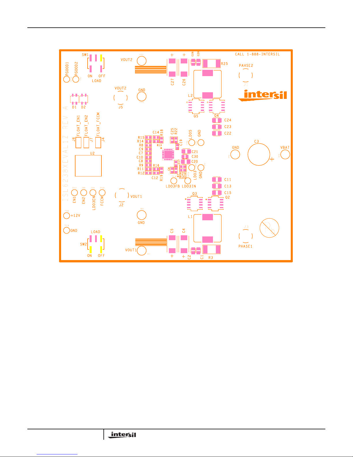
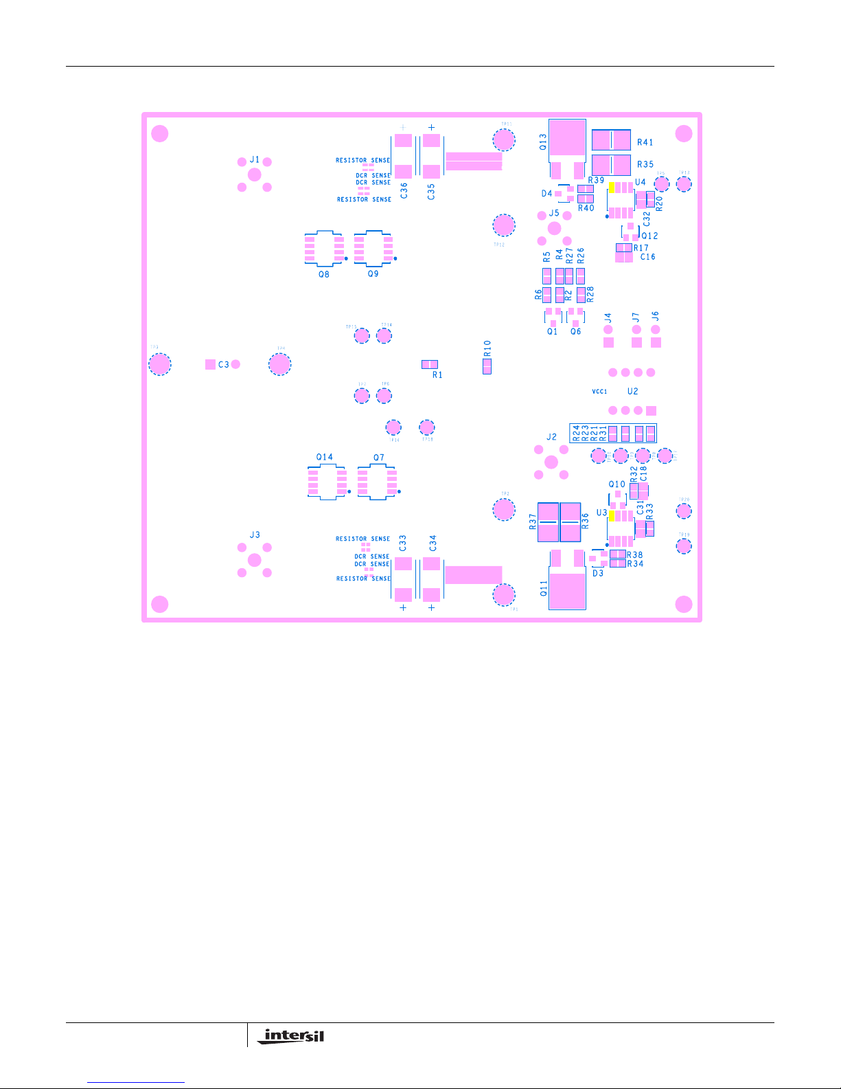
ISL6238xxxEVAL1Z Evaluation Board Layout
FIGURE 3. TOP SILKSCREEN
8
AN1396.0
July 31, 2008
Page 9
Application Note 1396
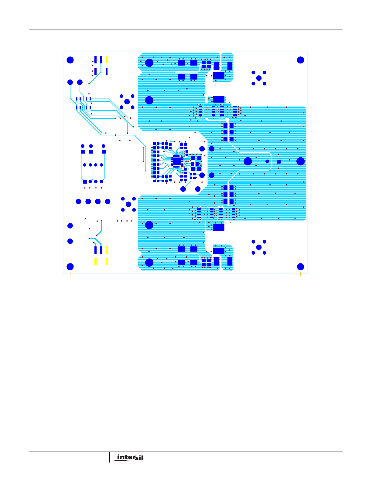
ISL6238xxxEVAL1Z Evaluation Board Layout (Continued)
FIGURE 4. BOTTOM SILKSCREEN
9
AN1396.0
July 31, 2008
Page 10
Application Note 1396
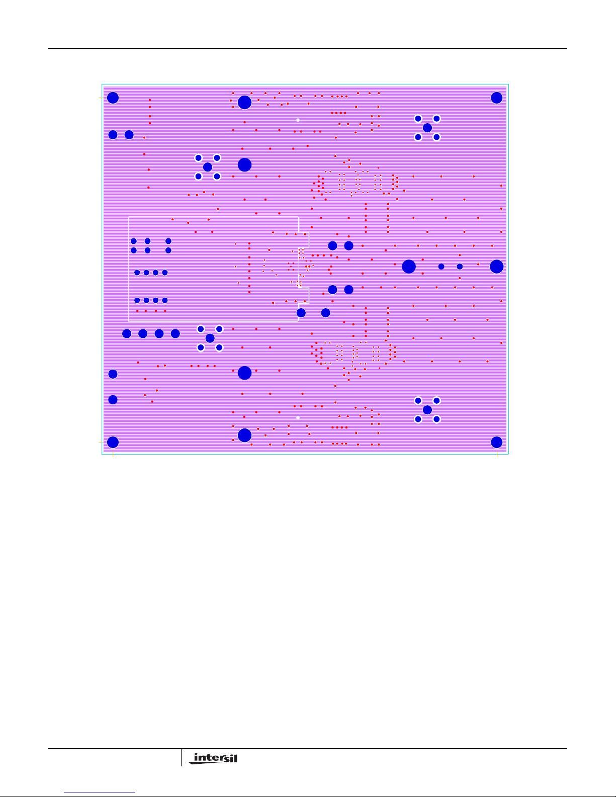
ISL6238xxxEVAL1Z Evaluation Board Layout (Continued)
10
FIGURE 5. LAYER 1
AN1396.0
July 31, 2008
Page 11
Application Note 1396
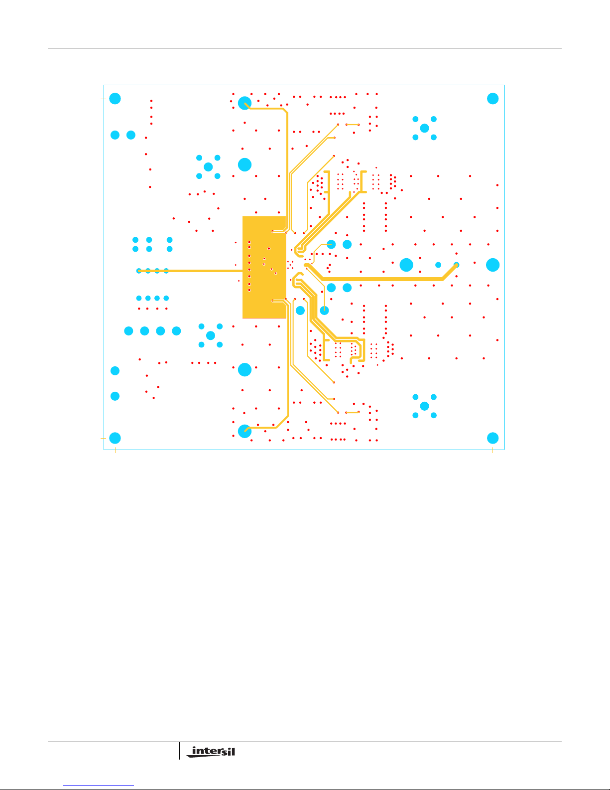
ISL6238xxxEVAL1Z Evaluation Board Layout (Continued)
11
FIGURE 6. LAYER 2
AN1396.0
July 31, 2008
Page 12
Application Note 1396
ISL6238xxxEVAL1Z Evaluation Board Layout (Continued)
12
FIGURE 7. LAYER 3
AN1396.0
July 31, 2008
Page 13
Application Note 1396
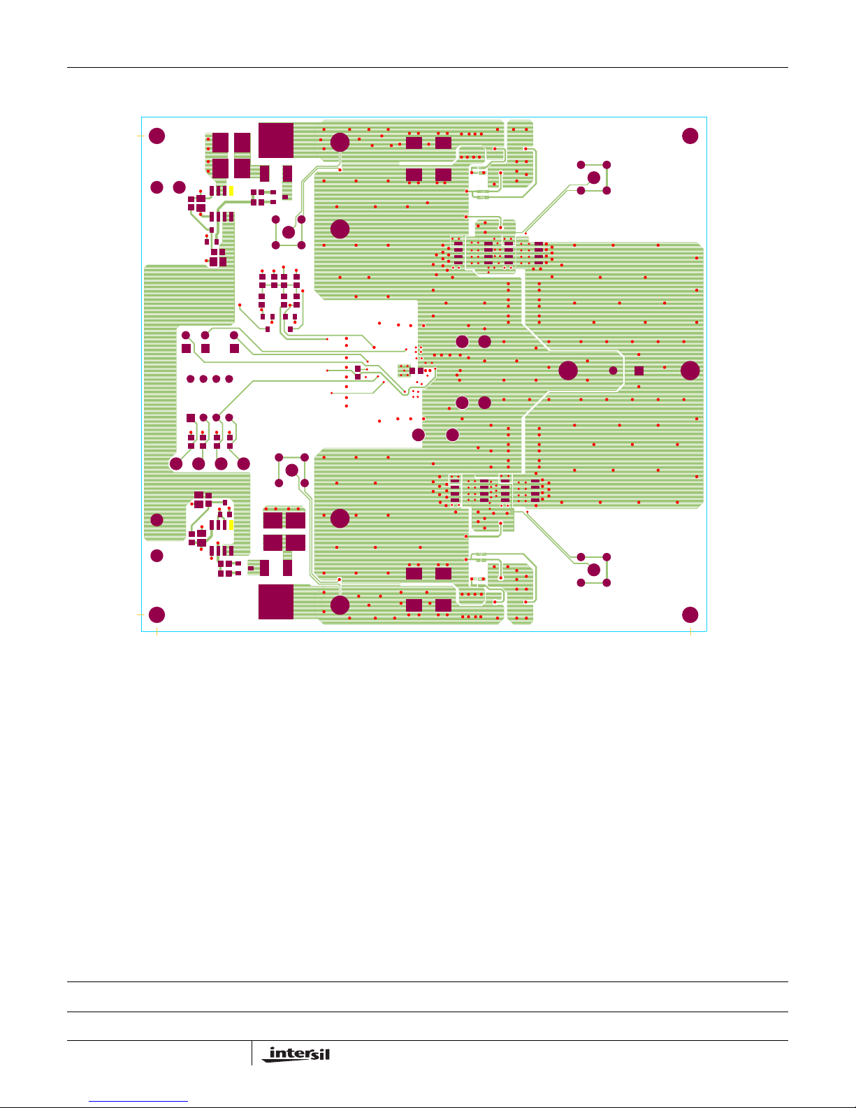
ISL6238xxxEVAL1Z Evaluation Board Layout (Continued)
FIGURE 8. LAYER 4
Intersil Corporation reserves the right to make changes in circuit design, software and/or specifications at any time without notice. Accordingly, the reader is cautioned to
verify that the Application Note or Technical Brief is current before proceeding.
For information regarding Intersil Corporation and its products, see www.intersil.com
13
AN1396.0
July 31, 2008
 Loading...