

Page 1
®
ISL6228EVAL3Z User Guide
Application Note May 17, 2007
Introduction
The ISL6228EVAL3Z evaluation board demonstrates the
performance of the ISL6228 dual-channel PWM controller.
The ISL6228 features Intersil's Robust Ripple Regulator (R
technology. Channel-1 output voltage is 1.5V or 1.8V,
pending the state of switch S5. Channel-2 output voltage is
1.8V. Each channel has an on-board dynamic-load
generator included for evaluating the transient-load
response. It applies a 300µs pulse of 4.5A load across V
and GND, and it applies a 300µs pulse of 5A load across
V
and GND.
O2
Contents of this document include:
• Recommended Test Equipment
• Interface Connections
• Switch Descriptions
• Test Point Descriptions
• Design Criteria
• Typical Performance
- Efficiency
- Start-up
- Shut-down
- Steady State, CCM
- Steady State, DCM
- Load-transient response
• Evaluation Board Documentation
- Bill of materials
- Schematic
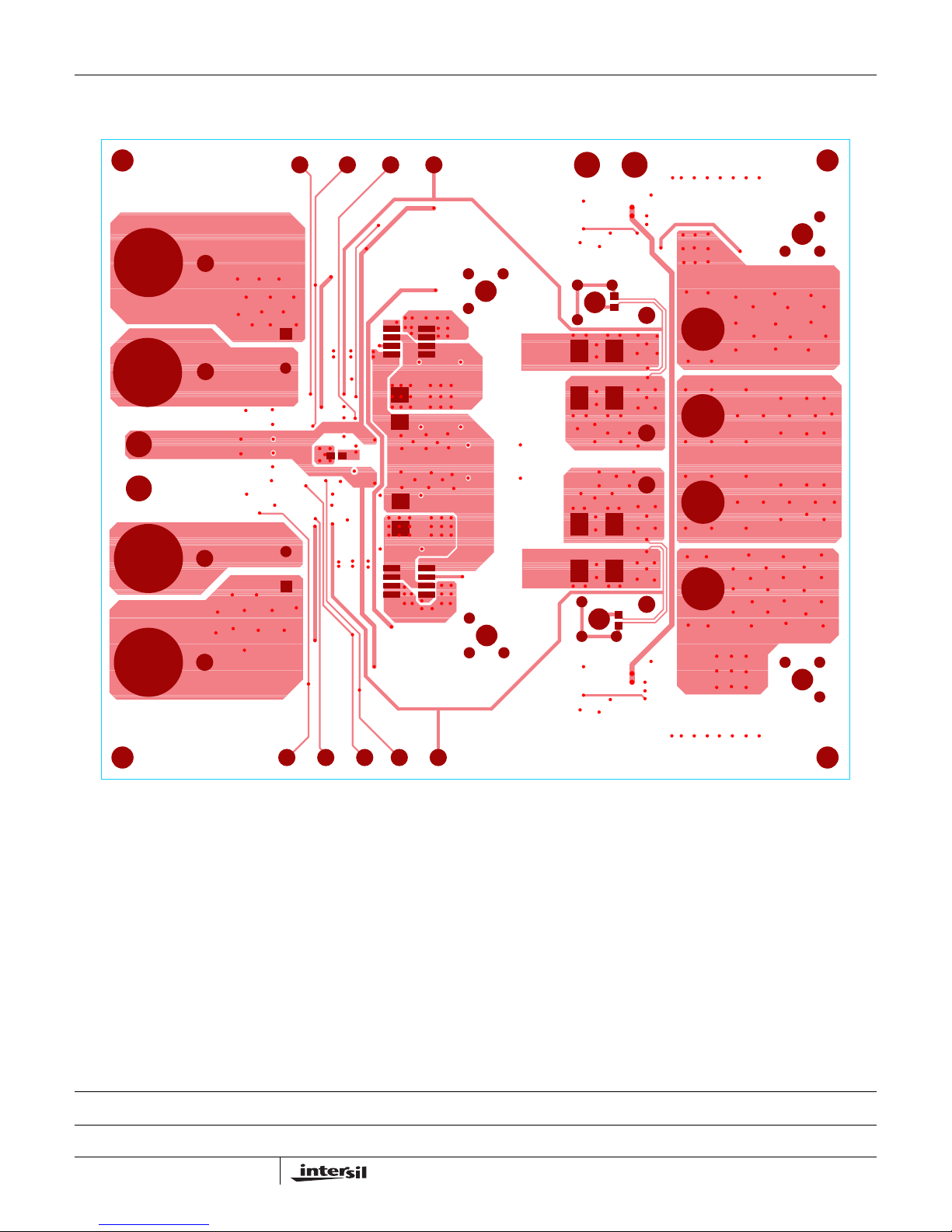
- Silk-screen plots
- Board layer plots
TABLE 1. DC/DC DESIGN CRITERIA
PARAMETER VALUE UNITS
V
IN
V
O
Full-load 8 ADC
PWM Frequency 270, 300 kHz
3.3 to 25 VDC
0.6 to 5 VDC
O1
AN1291.0
Author: Jia Wei
Recommended Equipment
• (QTY 2) Adjustable 25V, 3A Power Supply
3
)
• (QTY 1) Fixed 5V, 100mA Power Supply
• (QTY 1) Fixed 12V, 100mA Power Supply
• (QTY 1) Adjustable 20A Constant Current Electronic Load
• (QTY 1) Digital Voltmeter
• (QTY 1) Four-Channel Oscilloscope
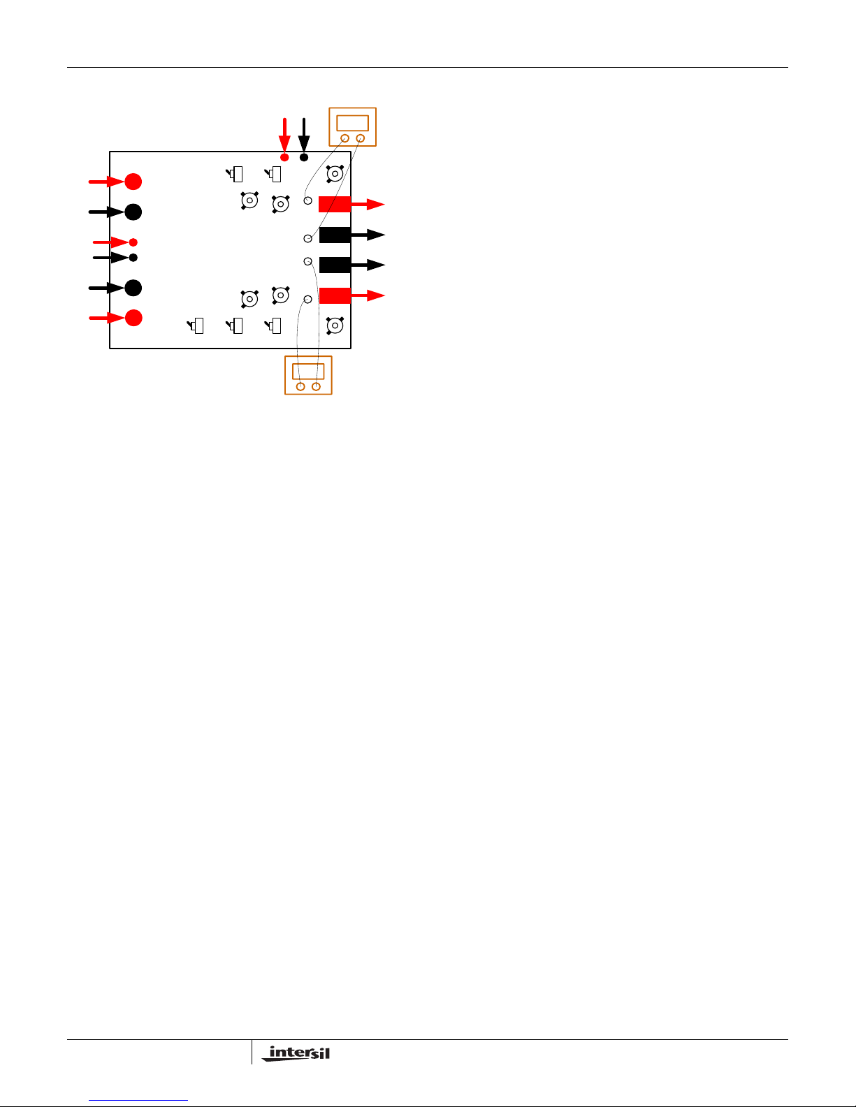
Interface Connections
•V
: Input voltage to the power stage of Channel-1
IN1
- J14: V
-TP20: V
- J14: V
-TP21: V
•V
IN2
-J1: V
-TP9: V
-J2: V
-TP10: V
•V
O1:
-J9: VO1 positive power output
-TP13: V
- J10: V
-TP14: VO1 return voltage sense
•V
: Regulated output voltage from Channel-2
O2
-J7: VO2 positive power output
-TP11: V
-J8: V
-TP12: V
• VCC: +5V input voltage
- TP1: 5V positive input
- TP2: 5V return input
• +12V: Input voltage for the dynamic-load generator
- TP15: 12V positive input
- TP16: 12V return input
positive power input
IN1
positive voltage sense
IN1
return power input
IN1
return voltage sense
IN1
: Input voltage to the power stage of Channel-2
positive power input
IN2
positive voltage sense
IN2
return power input
IN2
return voltage sense
IN2
Regulated output voltage from Channel-1
positive voltage sense
O1
return power output
O1
positive voltage sense
O2
return power output
O2
return voltage sense
O2
1
CAUTION: These devices are sensitive to electrostatic discharge; follow proper IC Handling Procedures.
1-888-INTERSIL or 1-888-468-3774
| Intersil (and design) is a registered trademark of Intersil Americas Inc.
All other trademarks mentioned are the property of their respective owners.
Copyright Intersil Americas Inc. 2007. All Rights Reserved
Page 2
Application Note 1291
Test Set-up
_
12V+
+
TP15 TP16
OFF
OFF
+
V
IN2
_
+
5V
_
_
V
IN1
+
J1
J2
TP1
TP2
J14
J13
VO1 INCREASE
ISL6228EVAL3Z
ON
J3
J4
OFF
ON
ON
S3
J5
J6
OFF
ON
S2
S1 S4S5
J11
TP11
J7
J8
TP12
J10
TP14
J9
TP13
J12
V
_
+
FIGURE 1. TEST SET-UP
Switch Descriptions
• S1: Channel-1 Enable
- OFF: Short the Channel-1 EN pin to GND (disable
PWM)
- ON: Allow the Channel-1 EN pin to pull-up to +5V
(enable PWM)
• S4: Channel-1 Dynamic Load
- OFF: On-board Channel-1 dynamic load disabled
- ON: On-board Channel-1 dynamic load enabled
• S5: Channel-1 V
-OFF: V
O1
- ON: Parallel R
• S2: Channel-2 Enable
- OFF: Short the Channel-2 EN pin to GND (disable
PWM)
- ON: Allow the Channel-2 EN pin to pull-up to +5V
(enable PWM)
• S3: Channel-2 Dynamic Load
- OFF: On-board Channel-2 dynamic load disabled
- ON: On-board Channel-2 dynamic load enabled
Increase
O
is 1.5V, determined by R15 and R23.
with R15. VO1 is 1.8V.
49
V
READING
V
O1
READING
Test-point Descriptions
• J4: Scope-probe socket for measuring PHASE1
_
V
O2
+
V
O2
_
_
V
O1
+
• J6: Scope-probe socket for measuring V
O1
• J12: Scope-probe socket for measuring the current of the
Channel-1 on-board transient-load emulator
• J3: Scope-probe socket for measuring the PHASE2 node
• J5: Scope-probe socket for measuring V
O2
• J11: Scope-probe socket for measuring the current of the
Channel-2 on-board transient-load emulator
• TP1: Monitor the 5V positive input
• TP2: Monitor the 5V return input
• TP3: Monitor the PGOOD2 pin
• TP4: Monitor the PGOOD1 pin
• TP5: The common node of R
and R20; Useful for
24
Channel-1 loop gain measurement.
• TP6: The common node of R
and R23; Useful for
25
Channel-2 loop gain measurement
• TP7: The V
side of R24; Useful for Channel-1 loop gain
O1
measurement.
• TP8: The V
side of R25; Useful for Channel-1 loop gain
O2
measurement.
• TP9: Monitor the V
• TP10: Monitor the V
• TP11: Monitor the positive V
• TP12: Monitor the V
• TP13: Monitor the positive V
• TP14: Monitor the V
positive input
IN1
return input
IN1
return output
O1
return output
O2
O1
O2
output
output
• TP15: Monitor the 12V positive input
• TP16: Monitor the 12V return input
• TP17: Monitor the EN1 pin
• TP18: Monitor the gate of transistor Q
18
• TP19: Monitor the EN2 pin
• TP20: Monitor the V
• TP21: Monitor the V
positive input
IN2
return input
IN2
2
AN1291.0
May 17, 2007
Page 3
Application Note 1291
Typical Performance
100
VIN = 8V
95
90
85
80
75
EFFICIENCY (%)
70
65
60
012345678
VIN = 12V
VIN = 19V
I
OUT
(A)
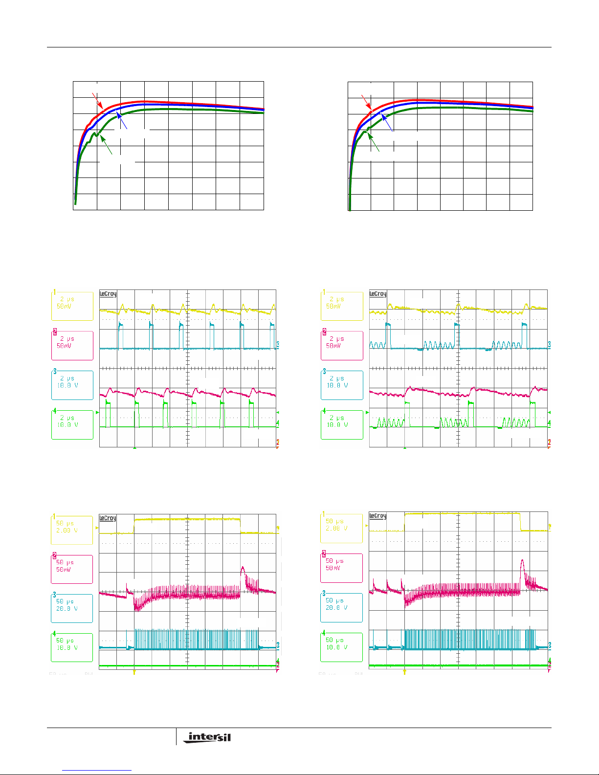
FIGURE 2. CHANNEL-1 EFFICIENCY AT VO= 1.5V FIGURE 3. CHANNEL-2 EFFICIENCY AT VO=1.8V
V
O1
100
VIN = 8V
95
90
85
80
75
EFFICIENCY (%)
70
65
60
01 234 5678
VIN = 12V
VIN = 19V
(A)
I
OUT
V
O1
V
O2
FIGURE 4. CCM STEADY-STA TE OPERA TION, V
V
= 1.5V, IO1=3A, VO2= 1.8A, IO2=4A
O1
I
O1
V
O1
PHASE1
PHASE2
= 12V,
IN
PHASE1
PHASE1
V
O2
FIGURE 5. DCM STEADY-STA TE OPERA T ION, V
V
= 1.5V, IO1= 0.5A, VO2= 1.8V, IO2=0.5A
O1
I
O2
V
O2
PHASE2
=12V,
IN
PHASE2
FIGURE 6. TRANSIENT RESPONSE, V
I
= 0.1A/4.6A @ 2.55A/µs
O
IN
3
= 19V, VO=1.5V,
FIGURE 7. TRANSIENT RESPONSE, V
I
= 0.1A/5.1A @ 2.55A/µs
O
= 19V, VO=1.8V,
IN
May 17, 2007
AN1291.0
Page 4
Typical Performance (Continued)
I
O1
V
O1
Application Note 1291
I
O2
V
O2
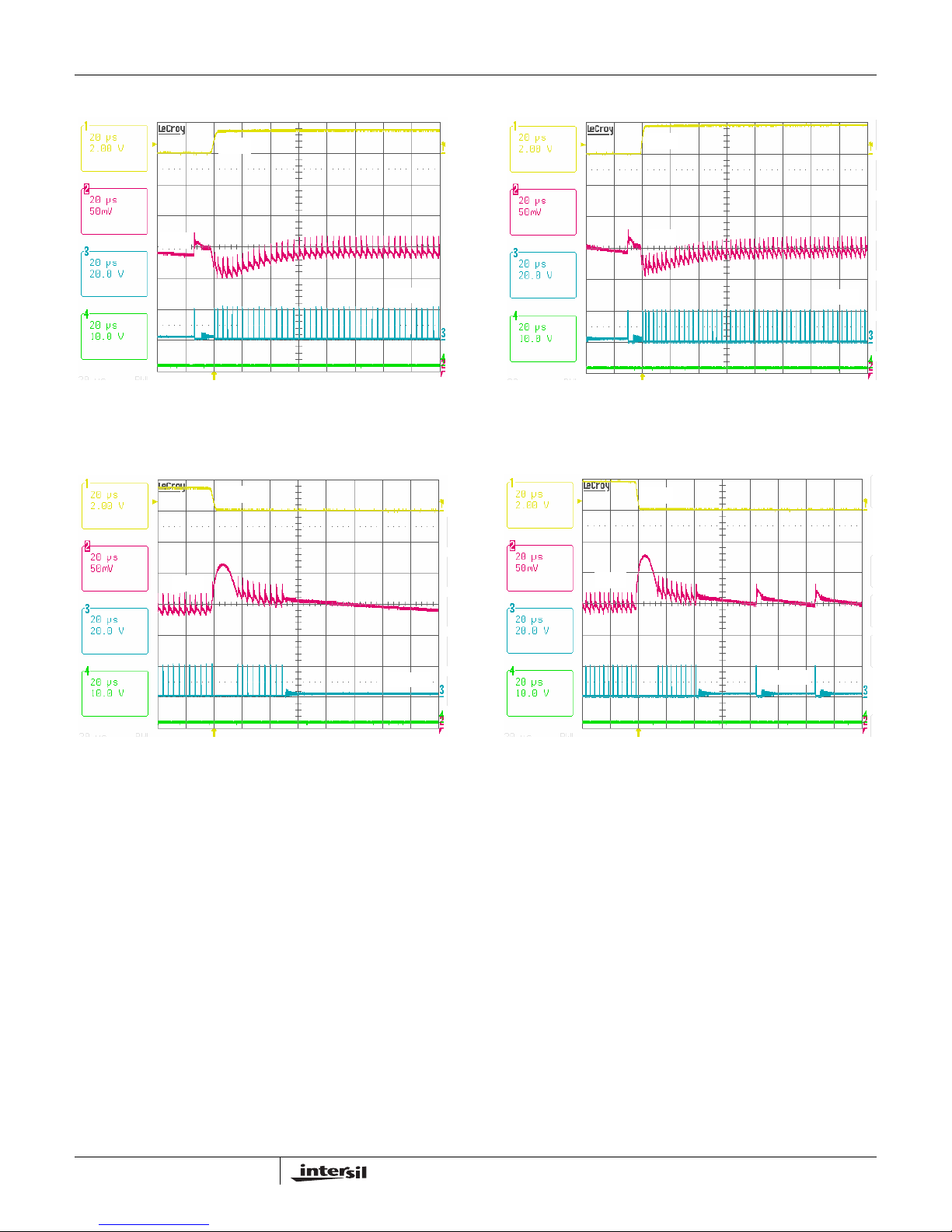
FIGURE 8. LOAD INSERTION RESPONSE, VIN=19V,
V
= 1.5V, IO= 0.1A/4.6A @ 2.55Aµs
O
I
O1
V
O1
FIGURE 10. LOAD RELEASE RESPONSE, V
V
= 1.5V, IO= 0.1A/4.6A @ 2.55A/µs
O
IN
= 19V,
PHASE1
PHASE1
FIGURE 9. LOAD INSERTION RESPONSE, V
V
= 1.8V, IO= 0.1A/5.1A @ 2.55A/µs
O
I
O2
V
O2
FIGURE 11. LOAD RELEASE RESPONSE, V
V
= 1.8V, IO= 0.1A/5.1A @ 2.55A/µs
O
IN
PHASE2
=19V,
IN
PHASE2
= 19V,
4
AN1291.0
May 17, 2007
Page 5
Application Note 1291
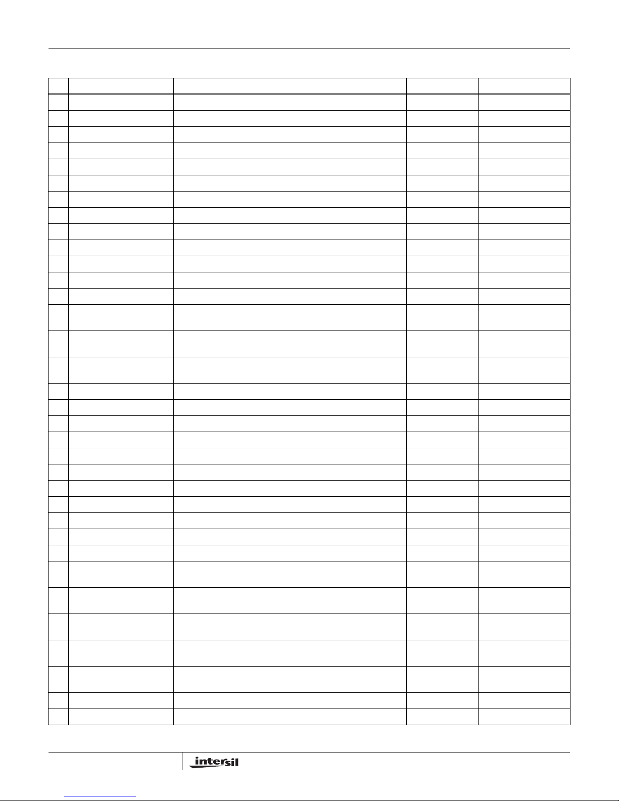
Bill of Materials
QTY REFERENCE DESCRIPTION MANUFACTURER PART NUMBER
0 DNP (C8, C9) CAP, RADIAL, 56µF, 25V, ROHS SANYO 25SP56M
2 C1, C3 CAP, SMD, 0603, 1000pF, 16V, 10%, X7R, ROHS VENKEL H1045-00102-16V10-T
5 C20, C21, C37, C40, C41 CAP, SMD, 0603, 0.1µF, 16V, 10%, X7R, ROHS MURATA H1045-00104-16V10-T
6 C2, C7, C30, C31, C36, C39 CAP, SMD, 0603, 1µF, 16V, 20%, Y5V, ROHS MURATA H1045-00105-16V20-T
2 C18, C19 CAP, SMD, 0603, 10µF, 6.3V, 20%, X5R, ROHS TDK H1045-00106-6R3V20-T
2 C5, C6 CAP, SMD, 0603, 2200pF, 50V, 10%, X7R, ROHS MURATA H1045-00222-50V10-T
2 C14, C15 CAP, SMD, 0603, 0.22µF, 16V, 10%, X7R, ROHS TDK H1045-00224-16V10-T
2 C4, C38 CAP, SMD, 0603, 0.22µF, 25V, 20%, X7R, ROHS VENKEL H1045-00224-25V20-T
2 C34, C35 CAP, SMD, 0805, 4.7µF, 16V, 10%, X5R, ROHS PANASONIC H1046-00475-16V10-T
0 DNP (C32, C33) CAP, SMD, 0805, 4.7µF, 16V, 10%, X5R, ROHS PANASONIC H1046-00475-16V10-T
2 C16, C17 CAP, SMD, 1206, 1µF, 25V, 20%, X5R, ROHS PANASONIC H1065-00105-25V20-T
4 C10 to C13 CAP, SMD, 1206, 10µF, 25V, 20%, X5R, ROHS PANASONIC H1065-00106-25V20-T
2 C24, C27 CAP-L O W ESR, SMD, D 3 L , 330µF, 6. 3 V, 2 0 % , POSCAP, ROHS SANYO 6TPF330M9L
0 DNP (C22, C23, C25, C26,
C28, C29)
2 J1, J13 CONN-GEN, BIND.POST, INSUL-RED, THMBNUT-GND JOHNSON
2 J2, J14 CONN-GEN, BIND.POST, INSUL-BLK, THMBNUT-GND JOHNSON
0 J3 to J6, J11, J12 CONN-SCOPE PROBE TEST POINT, PCB MNT TEKTRONIX 131-4353-00
4 TP1, TP2, TP15, TP16 CONN-TURRET, TERMINAL POST, TH, ROHS KEYSTONE 1514-2
15 TP3 to TP14, TP17 to TP19 CONN-MINI TEST POINT, VERTICAL, WHITE, ROHS KEYSTONE 5002
0 DNP (D3, D4) DIODE-SCHOTTKY, SMD, SMB, 2P, 40V , 3A LOW VF, Pb-FREE DIODES INC. B340LB-13-F-T
2 D5, D6 DIODE-S CH OT TK Y, SMD, SOT2 3, 3 P, 3 0V, 20 0m A, DU AL DI O DE FAIRCHILD BAT54S-T
2 D1, D2 LED, SMD, 4P, OTHER, POLARIZEDRED/GRN LUMEX SSL-LXA3025IGC
2 L1, L2 PWR CHOKE COIL, SMD, 13x12.9, 3.3µH, 20%, 18A, ROHS Vishay IHLP5050FDER3R3M01
2 U2, U3 IC-HI FREQ BRIDGE DRIVER, 8P, SOIC, 100V, ROHS INTERSIL HIP2100IBZ
1 U1 IC-DUAL CHANNEL CONTROLLER, 28P, QFN, ROHS INTERSIL ISL6228HRZ
5 Q11 to Q14, Q18 TRANSISTOR, N-CHANNEL, 3LD, SOT -23, 60V, 1 15mA, ROHS DIODES INC. 2N7002-7-F-T
0 DNP (Q5, Q10) TRANSISTOR-DUAL N-CHANNEL, 8P, SOIC, 30V, 7.5A, ROHS FAIRCHILD FDS6990AS
0 DNP (Q2, Q7) TRANSISTOR-MOS, N-CHANNEL, 8P, SOIC, 30V, 9.1mΩ RDS,
2 Q1, Q6 TRANSISTOR-MOS, N-CHANNEL, 8P, SOIC, 30V , 9.1mΩ RDS,
0 DNP (Q4, Q9) TRANSISTOR-MOS, N-CHANNEL, 8P, SOIC, 30V , 4.0mΩ RDS,
2 Q3, Q8 TRANSISTOR-MOS, N-CHANNEL, 8P, SOIC, 30V , 4.0mΩ RDS,
2 Q15, Q16 TRANSISTOR-MOS, N-CHANNEL, SMD, TO-252, 30V, 20A,
4 R9, R52, R53, R54 RES, SMD, 0603, 2Ω, 1/10W, 1%, TF, ROHS YAGEO H2511-00020-1/10W1-T
0 DNP (R12, R13, R57, R58) RESISTOR, SMD, 0603, 0Ω, 1/10W, TF, ROHS KOA H2511-00R00-1/10W-T
CAP-LOW ESR, S MD, D3L, 330µF, 6.3V, 2 0 %, POSCAP, ROHS SANYO 6TPF330M9L
111-0702-001
COMPONENTS
111-0703-001
IRF7821PBF
IRF7821PBF
IRF7832PBF
IRF7832PBF
ROHS
ROHS
ROHS
ROHS
ROHS
COMPONENTS
INTERNATIONAL
RECTIFIER
INTERNATIONAL
RECTIFIER
INTERNATIONAL
RECTIFIER
INTERNATIONAL
RECTIFIER
VISHAY SUD50N03-07-E3
5
AN1291.0
May 17, 2007
Page 6
Application Note 1291
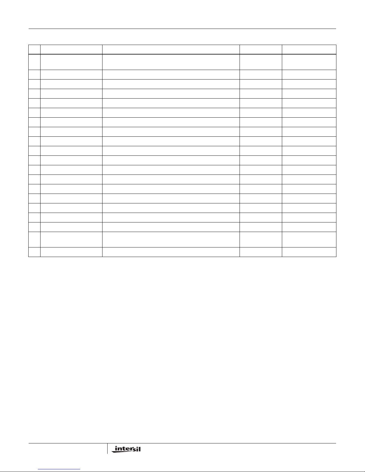
Bill of Materials (Continued)
QTY REFERENCE DESCRIPTION MANUFACTURER PART NUMBER
10 R10, R11, R24, R25, R48,
R50, R55, R56, R59, R60
5 R7, R8, R21, R22, R51 RES, SMD, 0603, 10k, 1/10W, 1%, TF, ROHS KOA H2511-01002-1/10W1-T
2 R35, R37 RES, SMD, 0603, 1.07k, 1/10W, 1%, TF, ROHS PANASONIC H2511-01071-1/10W1-T
1 R49 RES, SMD, 0603, 162k, 1/10W, 1%, TF, ROHS YAGEO H2511-01623-1/10W1-T
2 R26, R27 RES, SMD, 0603, 2k, 1/10W, 1%, TF, ROHS KOA H2511-02001-1/10W1-T
1 R3 RES, SMD, 0603, 20k, 1/10W, 1%, TF, ROHS KOA H2511-02002-1/10W1-T
1 R4 RES, SMD, 0603, 22.1k, 1/10W, 1%, TF, ROHS PANASONIC H2511-02212-1/10W1-T
2 R34, R36 RES, SMD, 0603, 2.49k, 1/10W, 1%, TF, ROHS KOA H2511-02491-1/10W1-T
1 R14 RES, SMD, 0603, 22.6k, 1/16W, 1%, TF, ROHS VENKEL H2511-02262-1/10W1-T
4 R1, R2, R5, R6 RES, SMD, 0603, 499Ω, 1/10W, 1%, TF, ROHS KOA H2511-04990-1/10W1-T
2 R30, R31 RES, SMD, 0603, 49.9k, 1/10W, 1%, TF, ROHS VENKEL H2511-04992-1/10W1-T
1 R15 RES, SMD, 0603, 53.6k, 1/10W, 1%, TF, ROHS YAGEO H2511-05362-1/10W1-T
4 R16, R17, R28, R29 RES, SMD, 0603, 5.76k, 1/10W, 1%, TF, ROHS ROHM H2511-05761-1/10W1-T
2 R18, R19 RES, SMD, 0603, 590Ω, 1/10W, 1%, TF, ROHS VENKEL H2511-05900-1/10W1-T
2 R20, R23 RES, SMD, 0603, 80.6k, 1/10W, 1%, TF, ROHS VENKEL H2511-08062-1/10W1-T
0 DNP (R32, R33) RES, SMD, 1206, 1.5Ω, 1/4W, 1%, TF, ROHS VENKEL H2513-001R5-1/4W1-T
4 R41, R43, R45, R47 RES, SMD, 1206, 1.5Ω, 1/4W, 1%, TF, ROHS VENKEL H2513-001R5-1/4W1-T
5 R38, R40, R42, R44, R46 RES, SMD, 1206, 1.8Ω, 1/4W, 1%, TF, ROHS VENKEL H2513-001R8-1/4W1-T
5 S1 to S5 SWITCH-TOGGLE, SMD, ULTRAMINI, 1P, SPST MINI C&K
4 J7 to J10 MTG HDWR, CBL.TERMINAL-LUG and SCREW, 6 to 14AWG BERG/FCI KPA8CTP
RESISTOR, SMD, 0603, 0Ω, 1/10W, TF, ROHS KOA H2511-00R00-1/10W-T
GT11MSCBE-T
COMPONENTS
6
AN1291.0
May 17, 2007
Page 7
7
AN1291.0
May 17, 2007
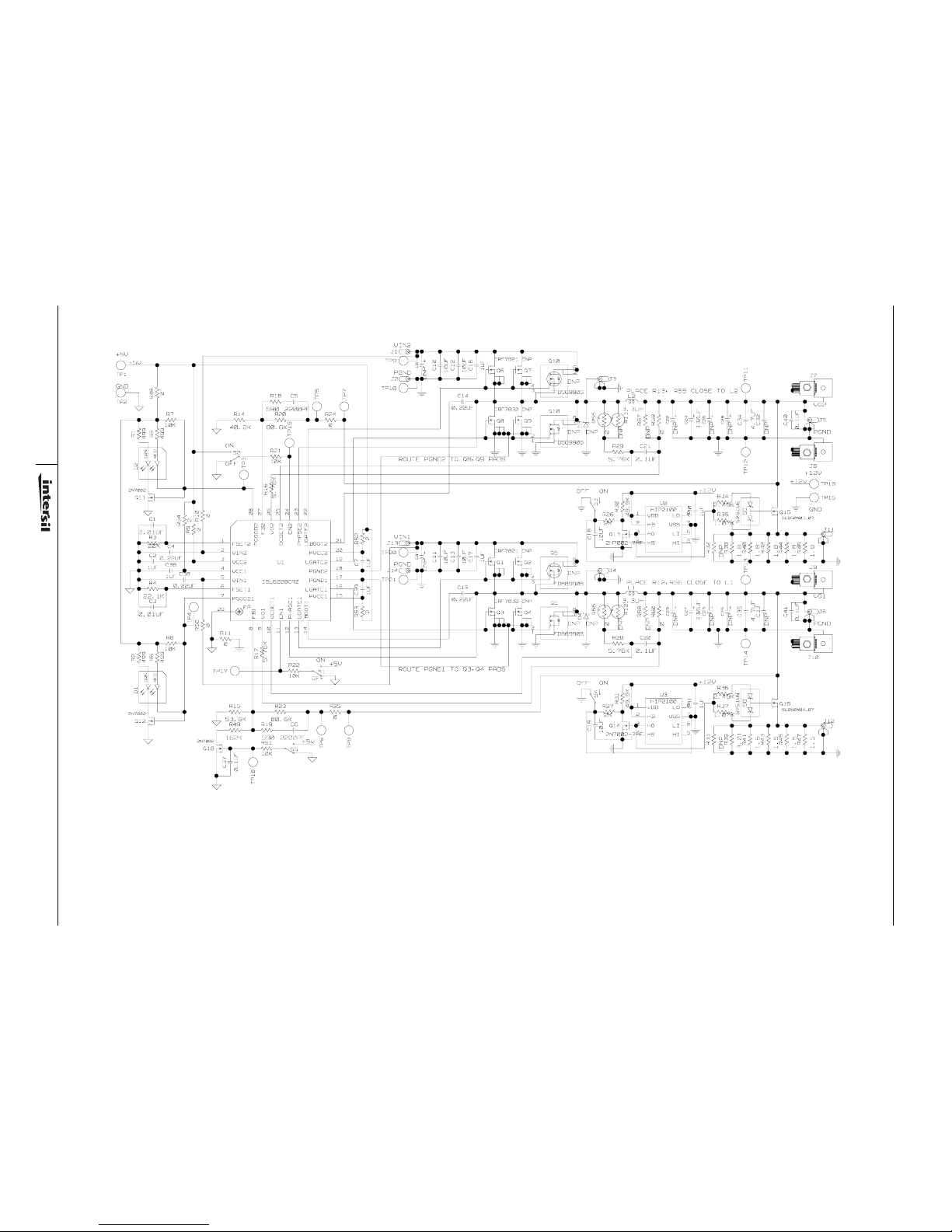
ISL6228EVAL3Z Evaluation Board Schematic
40.2K
IRF7821
DNP
0
DNP
0.1UF
APR 16, 2007ISL6228EVAL3Z REV.B
JIA WEI
DNP
0.01UF
162K 590
2200PF
20K
22.1K
ON
2200PF
OFF
1.5
2K
2K
1.07K
1.07K
2.49K
2.49K
3.3UH
PLACE R12,R56 CLOSE TO L1
3.01
1.8
DNP
DNP
1.8
DNP
1.5
1.5 1.8
1.8
1.8
1.5
DNP
0.01UF
OFF
ROUTE PGND1 TO Q3,Q4 PADS
80.6K
PLACE R13, R55 CLOSE TO L2
330UF
ON
80.6K
5.76K
GND
590
53.6K
ON
DNP
0.1UF
5.76K
5.76K
5.76K
DNP
0
4.7UF
DNP DNP
4.7UF
ROUTE PGND2 TO Q8,Q9 PADS
DNP
DNP
DNP
IRF7832
DNP
330UF
GND
DNP
DNP DNP
PGND
DNP
DNP
DNP
DNPDNP
VIN2
DNP
OFF
0
DNP
DNP
0
IRF7821
3.3UH
ON
PGND
+5V
1OF1
+12V
OFF
PGND
VO2
VO1
IRF7832
VIN1
PGND
Q18
10UF
C13
1UF
C39
2N7002-7-F
C29
Q16
SUD50N03_07
TP13
R44
J10
FDS6990S
R26
R30
49.9K
U2
+12V
R38
0.1UF
10K
Q2
R42
R32
8
D3
FDS6990S
3
6
R34
1UF
Q1
C14
TP19
TP18
TP8
J14
R52
21
20
19
18
BAT54S
J4
C18
10UF
R55
R13
3
4
C40
Q15
5
TP5
FDS6990S
C37
C6
4
C11
1UF
13
0
C10
TP20
J13
L2
R57
J6
0
C21
C28
Q8
22
R49
R17
R3
Q14
Q3
12
2
3
4
C4
U1
R8
1UF
0.22UF
2N7002
R15
R54
0
R10
0
10K
TP21
TP17
R48
S5
R51
J11
J12
TP16
TP15
C19
1
8
4
3
5
2
R27
R31
R39
R37
R36
D6
R47 R46
S3
Q13
7
6
TP4
TP7
R25
R24
TP2
TP10
TP9
R20
R18
C5
R23
S1
D1
R1
R5
R7
Q12
R6
R2
D2
C1
C3
J9
J8
C9
C16
C12
C31
J2
J1
Q4
1
2
8
6
5
1
2
7
4
Q7
0
+5V
10K
22
10UF
10UF
+12V
1UF
49.9K
2N7002-7-F
+5V
10K
1UF
0
10UF
499
499
499
+5V
2
2
C2
2N7002
Q11
R9
R4
0.22UF
5
281262725
17
15
11
9
8
7
6
29
J3
5
J7
8
0.1UF
10UF
3
L1
R40
TP3
Q10
+12V
Q10
0.1UF
R21
14
FDS6990S
R56
R12
1UF
Q6
Q9
C8
Q5
1
D4
7
Q5
R60
J5
C30
1UF
R35
BAT54S
D5
SUD50N03_07
2
C24C27
C23
C25
C22
C34
C32
C35
C33
TP11
TP12TP14
10
ISL6228CRZ
S2
TP1
R16
24
R14
C26
C7
R53
R59
R29
R19
10K
R50
R41
R45
C41
R43
HIP2100
TP6
R22
R11
C38
2N7002
499
C36
0.22UF
6
HIP2100
U3
R58
7
R33
S4
C20R28
C17
C15
0.22UF
16
23
HI
LO
HS
HO
LI
VSS
VDD
HB
HI
LO
HS
HO
LI
VSS
VDD
HB
EP
VIN2
VCC1
VIN1
PGOOD2
FSET2
VO2
FB2
EN2
OCSET2
PHASE2
UGATE2
BOOT2
PVCC2
LGATE2
PGND2
PGND1
LGATE1
PVCC1
BOOT1
UGATE1
PHASE1
EN1
OCSET1
VO1
FB1
PGOOD1
FSET1
VCC2
RED
GRN
RED
GRN
PAGE:
DATE:
TITLE:
ENGINEER:
A A
B B
C C
D
D
1
1
2
2
3
3
4
45
56
6
7
7
8
8
FIGURE 12. ISL6228EVAL3Z SCHEMATIC
Application Note 1291
Page 8
Application Note 1291
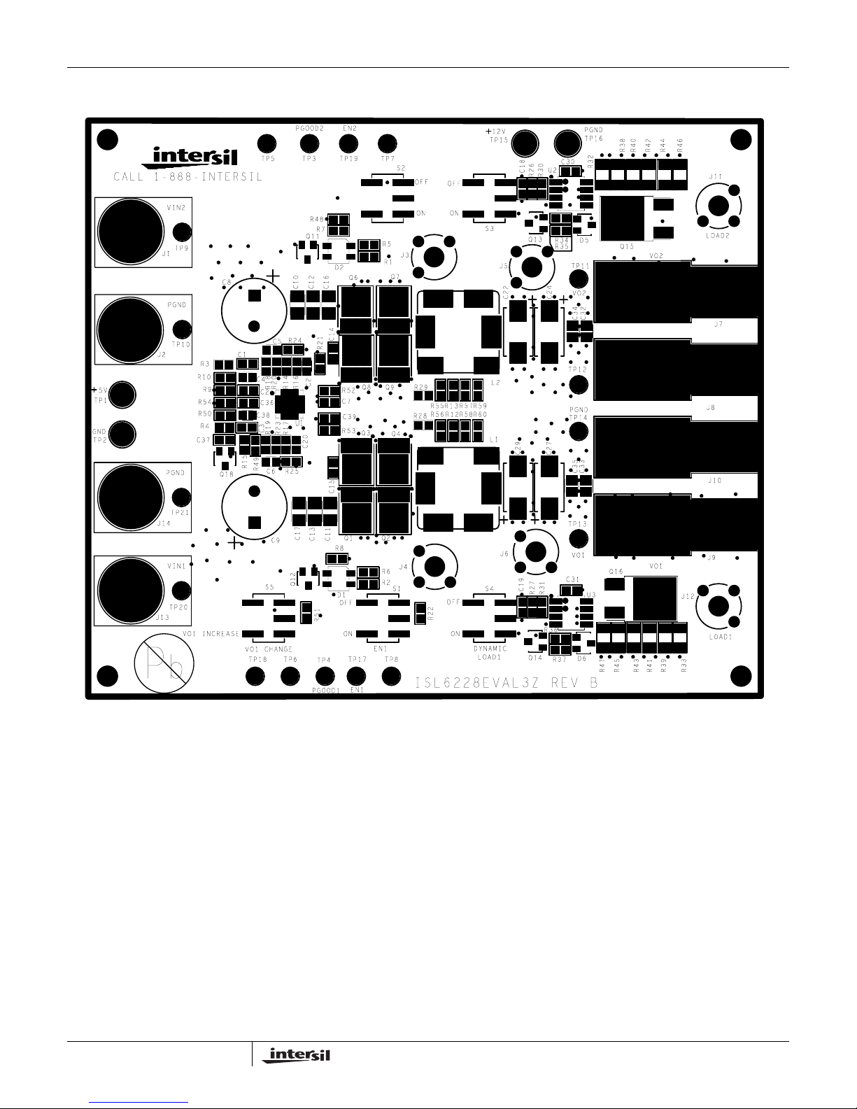
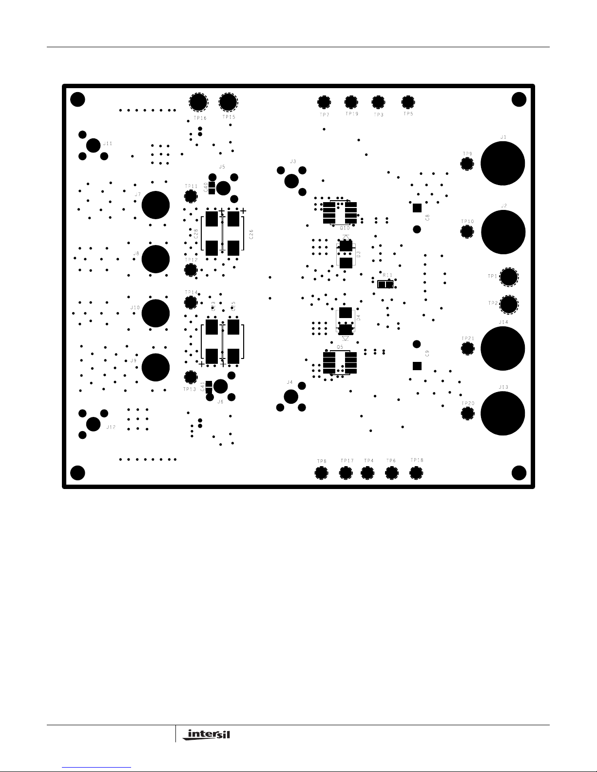
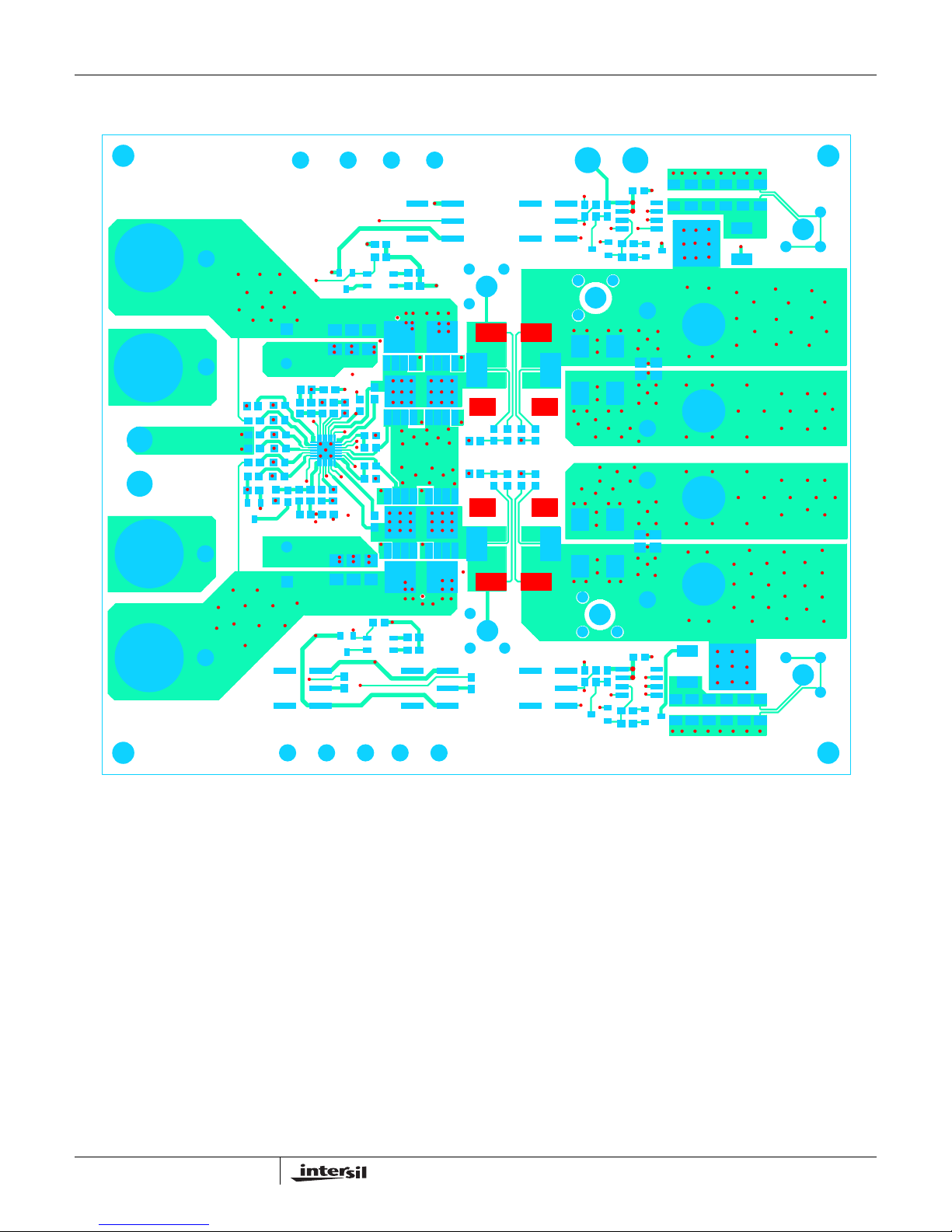
ISL6228EVAL3Z Evaluation Board Layout
8
FIGURE 13. TOP SILKSCREEN
AN1291.0
May 17, 2007
Page 9
Application Note 1291
ISL6228EVAL3Z Evaluation Board Layout (Continued)
9
FIGURE 14. BOTTOM SILKSCREEN
AN1291.0
May 17, 2007
Page 10
Application Note 1291
ISL6228EVAL3Z Evaluation Board Layout (Continued)
10
FIGURE 15. LAYER 1
AN1291.0
May 17, 2007
Page 11
Application Note 1291
ISL6228EVAL3Z Evaluation Board Layout (Continued)
11
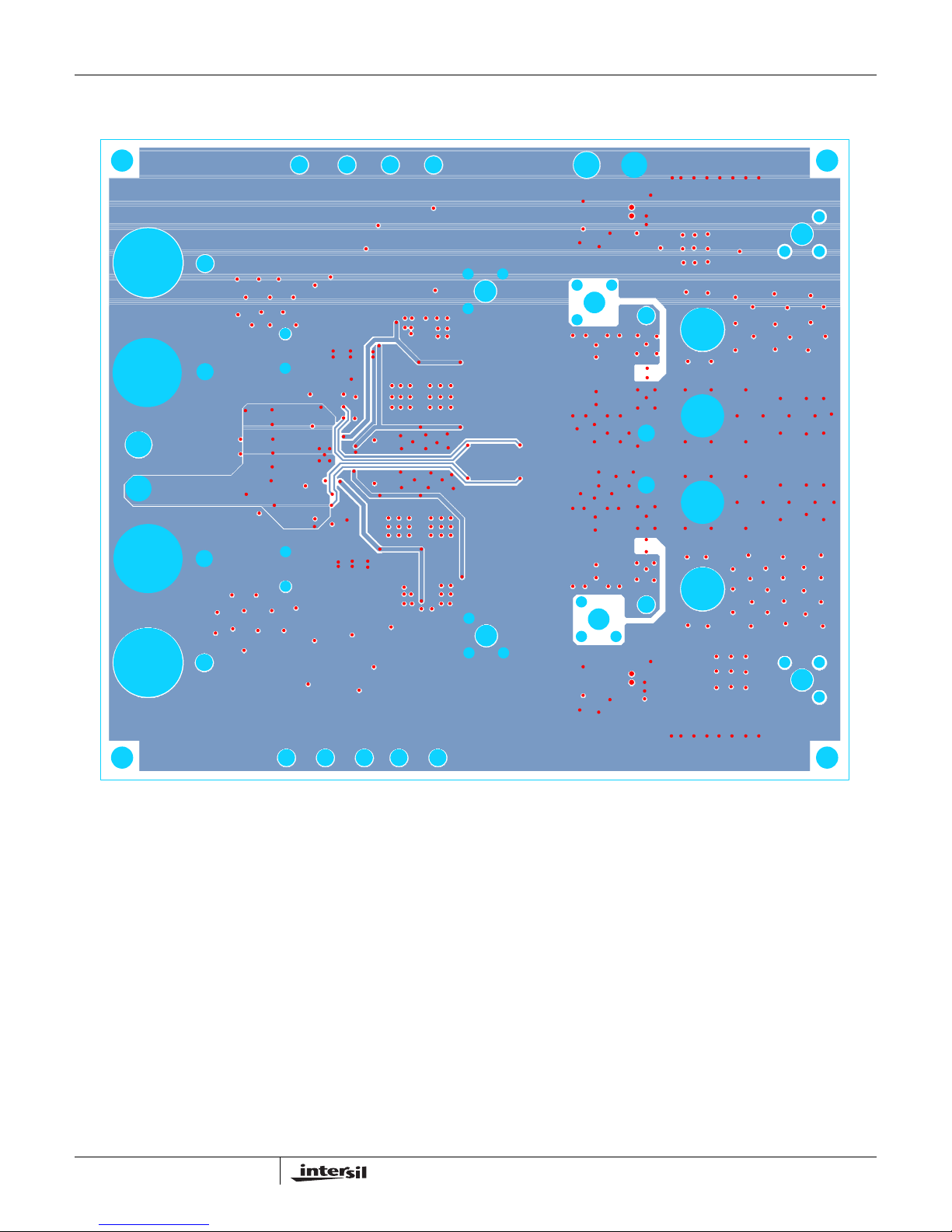
FIGURE 16. LAYER 2
AN1291.0
May 17, 2007
Page 12
Application Note 1291
ISL6228EVAL3Z Evaluation Board Layout (Continued)
12
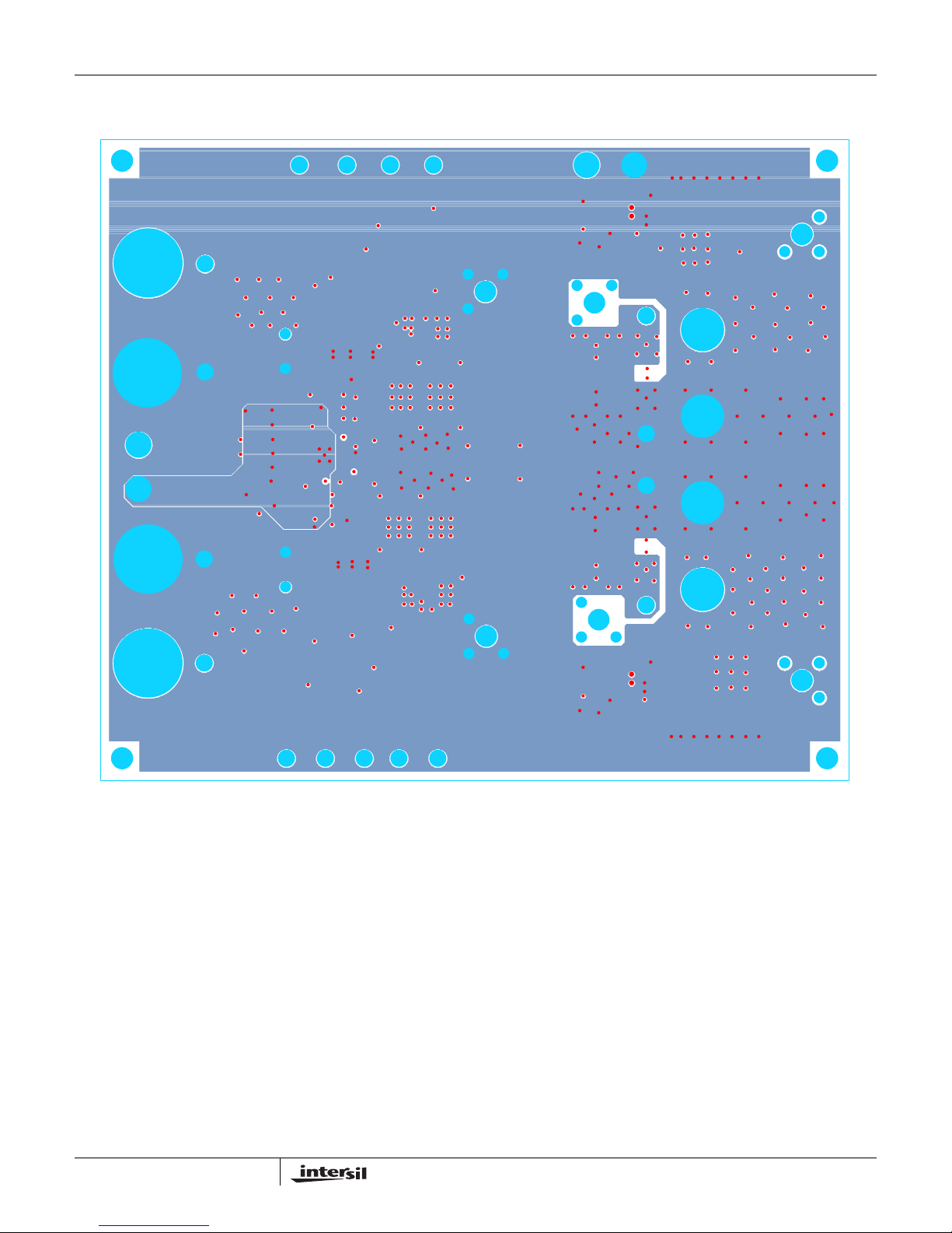
FIGURE 17. LAYER 3
AN1291.0
May 17, 2007
Page 13
Application Note 1291
ISL6228EVAL3Z Evaluation Board Layout (Continued)
Intersil Corporation reserves the right to make changes in circuit design, software and/or specifications at any time without notice. Accordingly, the reader is cautioned to
verify that the Application Note or Technical Brief is current before proceeding.
For information regarding Intersil Corporation and its products, see www.intersil.com
13
FIGURE 18. LAYER 4
AN1291.0
May 17, 2007
 Loading...