

Page 1
®
www.BDTIC.com/Intersil
ISL6161
Data Sheet July 2004
Dual Power Distribution Controller
The ISL6161 is a HOT SWAP dual supply power distribution
controller that can be used in PCI-Express applications.
Two external N-Channel MOSFETs are driven to distribute
and control power while providing load fault isolation. At turnon, the gate of each external N-Channel MOSFET is
charged with a 10µA current source. Capacitors on each
gate (see the Typical Application Diagram), create a
programmable ramp (soft turn-on) to control inrush currents.
A built in charge pump supplies the gate drive for the 12V
supply N-Channel MOSFET switch.
Over current protection is facilitated by two external current
sense resistors and FETs. When the current through either
resistor exceeds the user programmed value the controller
enters the current regulation mode. The time-out capacitor,
C
, starts charging as the controller enters the time out
TIM
period. Once C
N-Channel MOSFETs are latched off. In the event of a hard
and fast fault of at least three times the programmed current
limit level, the N-Channel MOSFET gates are pulled low
immediately before entering the time out period. The
controller is reset by a rising edge on the ENABLE
The ISL6161 constantly monitors both output voltages and
reports either one being low on the PGOOD output as a low.
The 12V PGOOD Vth is ~10.8V and the 3.3V Vth is ~2.8V
nominally.
charges to a 2V threshold, both the
TIM
pin.
FN9104.3
Features
• HOT SW AP Dual Pow er Distribution and Control f or +12V
and +3.3V
• Provides Fault Isolation
• Programmable Current Regulation Level
• Programmable Time Out
• Charge Pump Allows the Use of N-Channel MOSFETs
• Power Good and Over Current Latch Indicators
• Adjustable Turn-On Ramp
• Protection During Turn-On
• Two Levels of Current Limit Detection Provide Fast
Response to Varying Fault Conditions
•1µs Response Time to Dead Short
•3µs Response Time to 200% Current Overshoot
• Pb-free available
Applications
• PCI-Express Applications
• Power Distribution and Control
• Hot Plug, Hot Swap Components
TEMP. RANGE
PART NUMBER
(oC) PACKAGE
ISL6161CB -0 to 70 14 Ld SOIC M14.15
ISL6161CBZA
(See Note)
*Add “-T” suffix to part number for tape and reel packaging.
NOTE: Intersil Pb-free products employ special Pb-free material sets; molding
compounds/die attach materials and 100% matte tin plate termination finish, which
is compatible with both SnPb and Pb-free soldering operations. Intersil Pb-free
products are MSL classified at Pb-free peak reflow temperatures that meet or
exceed the Pb-free requirements of IPC/JEDEC J Std-020B.
-0 to 70 14 Ld SOIC
(Pb-free)
PKG.
DWG. #
M14.15
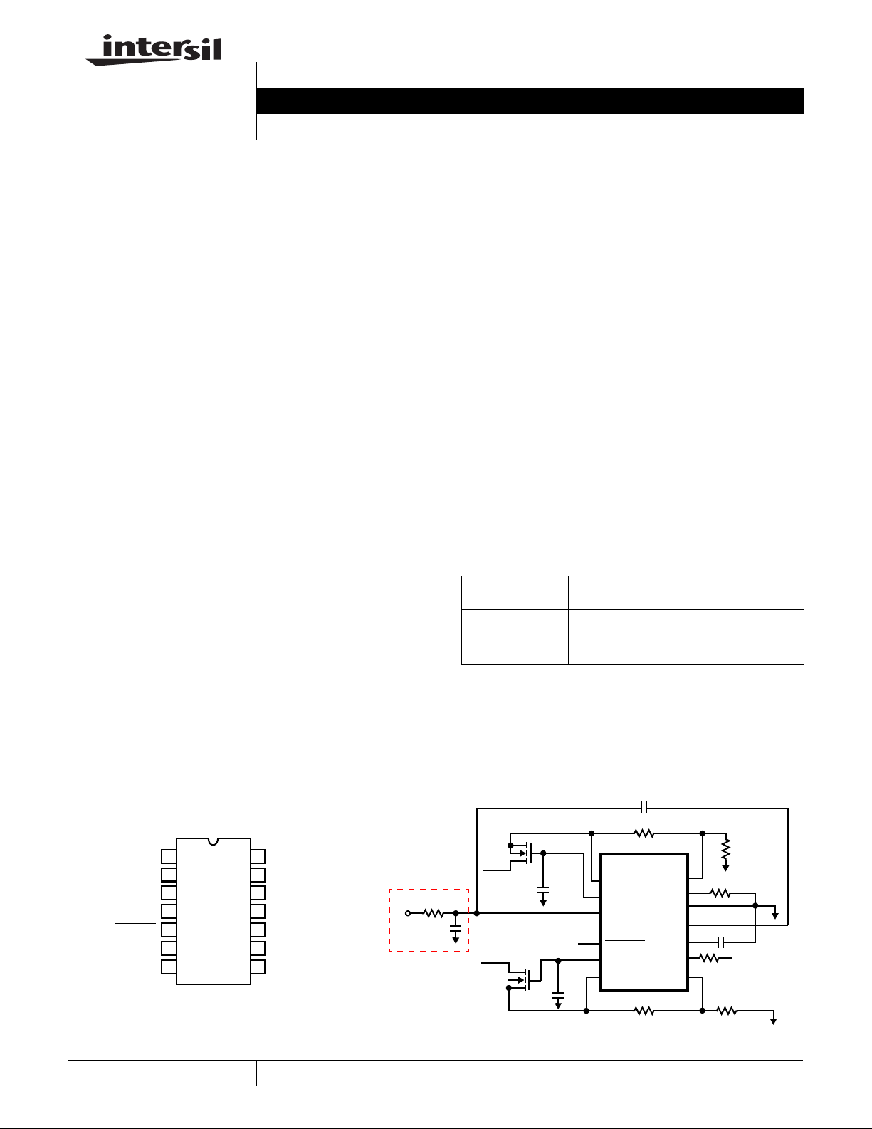
Pinout
Typical Application Diagram
ISL6161 (SOIC)
TOP VIEW
12VS
12VG
V
DD
NC
ENABLE
3VG
3VS
1
2
3
4
5
6
7
12VISEN
14
R
13
ILIM
GND
12
C
11
PUMP
C
10
TIM
PGOOD
9
3VISEN
8
1
Copyright © Intersil Americas Inc. 2001, 2003-2004. All Rights Reserved. Hot Plug™ is a trademark of Core International, Inc.
OPTIONAL
R
FILTER
V
DD
C
FILTER
CAUTION: These devices are sensitive to electrostatic discharge; follow proper IC Handling Procedures.
1-888-INTERSIL or 321-724-7143
12V
C
GATE
ENABLE
3.3V
C
GATE
| Intersil (and design) is a registered trademark of Intersil Americas Inc.
All other trademarks mentioned are the property of their respective owners.
INPUT
R
SENSE
ISL6161
12VS
12VG
V
DD
ENABLE
3VG
3VS
R
SENSE
C
PUMP
12VISEN
R
ILIM
GND
C
PUMP
C
TIM
PGOOD
3ISEN
R
ILIM
R
C
TIM
LOAD
R
3.3V
LOAD
Page 2
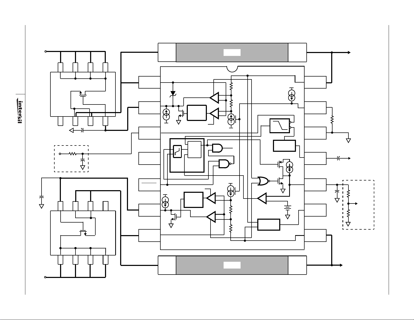
Simplified Schematic
www.BDTIC.com/Intersil
12VIN
R
SENSE
TO LOAD
10µA
12ISEN
R
ILIM
GND
C
PUMP
C
TIM
PGOOD
3ISEN
R
ILIM
ISL6161
C
PUMP
C
TIM
TO V
OPTIONAL
DD
OC
LATCH
2
C
GATE
OPTIONAL
R
FILTER
C
FILTER
C
GATE
VDD
12VS
12VG
VDD
NC
ENABLE
3VG
3VS
OC
CLIM
+
-
FALLING
EDGE
10µA
18V
RISING
EDGE
RESET
12V
10µA
DELAY
ENABLE
R
QN
R
Q
S
ENABLE
FALLING
EDGE
DELAY
+
3X
+
-
CLIM
+
OC
3X
R
2R
18V
ENABLE
12V
2R
R
POR
+
-
PGOOD
100µA
QPUMP
12V
2V
12V
+
-
5VIN
ISL6161
R
SENSE
TO LOAD
Page 3
ISL6161
www.BDTIC.com/Intersil
Pin Descriptions
PIN # SYMBOL FUNCTION DESCRIPTION
1 12VS 12V Source Connect to source of associated external N-Channel MOSFET switch to sense output
2 12VG 12V Gate Connect to the gate of associated N-Channel MOSFET switch. A capacitor from this node
3V
4 NC Not Connected
5 ENABLE
6 3VG 3V Gate Connect to the gate of the external 3V N-Channel MOSFET. A capacitor from this node to
7 3VS 3 Source Connect to the source side of 3V external N-Channel MOSFET switch to sense output
8 3VISEN 3V Current Sense Connect to the load side of the 3V sense resistor to measure the voltage drop across this
9 P GOOD Power Good indicator Indicates that all output voltages are within specification. PGOOD is driven by an open drain
DD
Chip Supply Connect to 12V supply. This can be either connected directly to the +12V rail supplying the
Enable / Reset ENABLE is used to turn-on and reset the chip. Both outputs turn-on when this pin is driven
voltage.
to ground sets the turn-on ramp. At turn-on this capacitor will be charged to ~17.4V by a
10µA current source.
load voltage or to a dedicated V
V
decoupling must be paid to prevent sagging as heavy loads are switched on.
DD
low. After a current limit time out, the chip is reset by the rising edge of a reset signal applied
to the ENABLE
5V open drain and standard logic.
ground sets the turn-on ramp. At turn-on this capacitor will be charged to ~11.4V by a 10µA
current source.
voltage.
resistor between 3VS and 3VISEN pins.
N-Channel MOSFET. It is pulled low when any output is not within specification.
pin. This input has 100µA pull up capability which is compatible with 3V and
+12V supply. If the former is chosen special attention to
DD
10 C
11 C
12 GND Chip Ground
13 R
14 12VISEN 12V Current Sense Connect to the load side of sense resistor to measure the v olt age drop acr oss this resisto r.
TIM
PUMP
ILIM
Current Limit Timing
Capacitor
Charge Pump
Capacitor
Current Limit Set
Resistor
Connect a capacitor from this pin to ground. This capacitor controls the time between the
onset of current limit and chip shutdown (current limit time-out). The duration of current limit
time-out (in seconds) = 200kΩ x C
Connect a 0.1µF capacitor between this pin and VDD (pin 3). Provides charge storage for
12VG drive.
A resistor connected between this pin and ground determines the current level at which
current limit is activated. This current is determined by the ratio of the R
sense resistor (R
). The ISL6161 is limited to a 10kΩ min. value (OC Vth = 100mV) resistor whereas
R
SENSE
the ISL6161 can accommodate a 5kΩ resistor for a lower OC Vth (50mV).
). The current at current limit onset is equal to 10µA x (R
SENSE
TIM
(Farads).
resistor to the
ILIM
ILIM
/
3
Page 4

ISL6161
www.BDTIC.com/Intersil
Absolute Maximum Ratings T
VDD . . . . . . . . . . . . . . . . . . . . . . . . . . . . . . . . . . . . . . .-0.3V to +16V
12VG, C
12VISEN, 12VS . . . . . . . . . . . . . . . . . . . . . . . . . . -5V to V
3VISEN, 3VS . . . . . . . . . . . . . . . . . . . . . . . . . . . . . . . . . . -5V to 7.5V
PGOOD, R
ENABLE
ESD Classification . . . . . . . . . . . . . . . . . . . . . . . . . . . . 2kV (Class 2)
. . . . . . . . . . . . . . . . . . . . . . . . . . . . . . . .-0.3V to 21V
PUMP
. . . . . . . . . . . . . . . . . . . . . . . . . . . . . . . -0.3V to 7.5V
ILIM
, C
, 3VG . . . . . . . . . . . . . . . . . . . . .-0.3V to VDD + 0.3V
TIM
=25oC Thermal Information
A
Thermal Resistance (Typical, Note 1) θ
DD
+ 0.3V
SOIC Package . . . . . . . . . . . . . . . . . . . . . . . . . . . . . 67
Maximum Junction Temperature (Plastic Package) . . . . . . . .150
Maximum Storage Temperature Range. . . . . . . . . . -65
Maximum Lead Temperature (Soldering 10s) . . . . . . . . . . . . .300
(SOIC - Lead Tips Only)
(oC/W)
JA
o
C to 150oC
o
o
Operating Conditions
VDD Supply Voltage Range. . . . . . . . . . . . . . . . . .+10.5V to +13.2V
Temperature Range (T
CAUTION: Stresses above those listed in “Absolute Maximum Ratings” may cause permanent damage to the device. This is a stress only rating and operation of the
device at these or any other conditions above those indicated in the operational sections of this specification is not implied.
NOTES:
1. θ
is measured with the component mounted on a high effective thermal conductivity test board in free air. See Tech Brief TB379 for details.
JA
2. All voltages are relative to GND, unless otherwise specified.
Electrical Specifications V
PARAMETER SYMBOL TEST CONDITIONS MIN TYP MAX UNITS
12V CONTROL SECTION
Current Limit Threshold Voltage
(Voltage Across Sense Resistor)
3X Current Limit Threshold Voltage
(Voltage Across Sense Resistor)
±20% Current Limit Response Time
(Current within 20% of Regulated Value)
±10% Current Limit Response Time
(Current within 10% of Regulated Value)
±1% Current Limit Response Time
(Current within 1% of Regulated Value)
Response Time To Dead Short RT
Gate Turn-On Time t
Gate Turn-On Current I
3X Gate Discharge Current 3XdisI 12VG = 18V 0.5 0.75 - A
12V Under Voltage Threshold 12V
Charge Pumped 12VG Voltage V12VG C
3.3V CONTROL SECTION
Current Limit Threshold Voltage
(Voltage Across Sense Resistor)
3X Current Limit Threshold Voltage
(Voltage Across Sense Resistor)
±20% Current Limit Response Time
(Current within 20% of regulated value)
±10% Current Limit Response Time
(Current within 10% of Regulated Value)
±1% Current Limit Response Time
(Current within 1% of Regulated Value)
Response Time To Dead Short RT
) . . . . . . . . . . . . . . . . . . . . . . . . 0oC to 70oC
A
= 12V, CVG = 0.01µF, C
DD
Unless Otherwise Specified
V
IL12V
3XV
IL12VRILIM
20%iLrt 200% Current Overload, R
10%iLrt 200% Current Overload, R
1%iLrt 200% Current Overload, R
SHORTC12VG
ON12V
ON12V
V
IL3V
3XV
SHORTCVG
R
ILIM
R
ILIM
R
ILIM
R
SHORT
R
SHORT
R
SHORT
C
12VG
C
12VG
VUV
PUMP
R
ILIM
R
ILIM
IL3VRILIM
R
ILIM
200% Current Overload, R
R
SHORT
200% Current Overload, R
R
SHORT
200% Current Overload, R
R
SHORT
= 0.1µF, R
TIM
= 10kΩ 92 100 108 mV
= 5kΩ 47 53 59 mV
= 10kΩ 250 300 350 mV
= 5kΩ 100 165 210 mV
= 6.0Ω
= 6.0Ω
= 6.0Ω
= 0.01µF - 500 1000 ns
= 0.01µF-12-ms
= 0.01µF 8 10 12 µA
= 0.1µF 16.8 17.3 17.9 V
= 10kΩ 92 100 108 mV
= 5kΩ 47 53 59 mV
= 10kΩ 250 300 350 mV
= 5kΩ 100 155 210 mV
= 2.5Ω
= 2.5Ω
= 2.5Ω
= 0.01µF - 500 800 ns
SENSE
= 0.1Ω, C
= 10kΩ,
ILIM
= 10kΩ,
ILIM
= 10kΩ,
ILIM
= 10kΩ,
ILIM
= 10kΩ,
ILIM
= 10kΩ,
ILIM
= 220µF, ESR = 0.5Ω, TA = TJ = 0oC to 70oC,
BULK
-2-µs
-4-µs
-10-µs
10.5 10.8 11.0 V
-2-µs
-4-µs
-10-µs
C
C
4
Page 5

ISL6161
www.BDTIC.com/Intersil
Electrical Specifications V
PARAMETER SYMBOL TEST CONDITIONS MIN TYP MAX UNITS
Gate Turn-On Time t
Gate Turn-On Current I
3X Gate Discharge Current 3XdisI C
3.3V Under Voltage Threshold 3.3V
3.3VG High Voltage 3VG 11.2 11.9 - V
SUPPLY CURRENT AND IO SPECIFICATIONS
V
Supply Current I
DD
POR Rising Threshold 9.5 10.0 10.7 V
V
DD
POR Falling Threshold 9.3 9.8 10.3 V
V
DD
Current Limit Time-Out T
ENABLE
ENABLE
ENABLE
ENABLE
Current Limit Time-Out Threshold (C
C
C
C
R
Charge Pump Output Current Qpmp_Io C
Charge Pump Output Voltage Qpmp_Vo No load 17.2 17.4 - V
Charge Pump Output Voltage - Loaded Qpmp_VIo Load current = 100µA 16.2 16.7 - V
Charge Pump POR Rising Threshold Qpmp+Vth 15.6 16 16.5 V
Charge Pump POR Falling Threshold Qpmp-Vth 15.2 15.7 16.2 V
Pull-up Voltage PWRN_V ENABLE pin open 1.8 2.4 3.2 V
Rising Threshold PWR_Vth 1.1 1.5 2 V
Hysteresis PWR_hys 0.1 0.2 0.3 V
Pull-Up Current PWRN_I 60 80 100 µA
Charging Current C
TIM
Discharge Current C
TIM
Pull-Up Current C
TIM
Pin Current Source Output R
ILIM
= 12V, CVG = 0.01µF, C
DD
Unless Otherwise Specified (Continued)
ON3V
ON3V
VUV
VDD
ILIM
)C
TIM
_Vth 1.8 2 2.2 V
TIM
_I 8 10 12 µA
TIM
_disI 1.7 2.6 3.5 mA
TIM
_disI V
TIM
_Io 90 100 110 µA
ILIM
= 0.1µF, R
TIM
C
= 0.01µF-5-ms
VG
C
= 0.01µF 8 10 12 µA
VG
= 0.01µF, ENABLE = Low 0.5 0.75 - A
VG
C
= 0.1µF162024ms
TIM
= 8V 3.556.5mA
CTIM
= 0.1µF, C
PUMP
= 0.1Ω, C
SENSE
= 16V 320 560 800 µA
PUMP
= 220µF, ESR = 0.5Ω, TA = TJ = 0oC to 70oC,
BULK
2.7 2.85 3.0 V
4810mA
ISL6161 Description and Operation
The ISL6161 is a multi featured +12V and +3.3V dual power
supply distribution controller, features include programmable
current regulation (CR) limiting and time to latch off .
At turn-on, the gate capacitor of each external N-Channel
MOSFET is charged with a 10µA current source. These
capacitors create a programmable ramp (soft turn-on). A
charge pump supplies the gate drive for the 12V supply control
FET switch driving that gate to 17V .
The load currents pass through two external current sense
resistors. When the voltage across either resistor quickly
exceeds the user programmed Current Regulation voltage
threshold (CRVth) lev el, the controller enters current regulation.
The CRVth is set by the e xternal resistor value on R
this time the time-out capacitor, C
, starts charging with a
TIM
10µA current source and the controller enters the time out
period. The length of the time out period is set by the single
external capacitor (see Table 2) placed from the C
10) to ground and is characterized by a lowered gate drive
5
ILIM
TIM
pin. At
pin (pin
voltage to the appropriate external N-Channel MOSFET. Once
C
charges to 2V, an internal comparator is tripped resulting
TIM
in both N-Channel MOSFETs being latched off. If the voltage
across the sense resistors rises slowly in response to an OC
condition, then the CR mode is entered at ~95% of the
programmed CR level. This difference is due to the necessary
hysteresis and response time in the CR control circui try.
Table 1 shows Rsense and Rilim recommendations and
resulting CR level f or the PCI-Express add-in card connector
sizes specified.
TABLE 1.
SENSE
12V R
(mΩ),
NOMINAL
CR (A)
3.3V R
NOMINAL
(mΩ),
CR (A)
PCI-EXPRESS
ADD-IN CARD
CONNECTOR
X1 10 30, 3.3 150, 0.7 100
R
ILIM
(kΩ)
4.99 15, 3.5 90, 0.6 53
SENSE
NOMINAL
CRVth
(mV)
Page 6

ISL6161
www.BDTIC.com/Intersil
TABLE 1. (Continued)
SENSE
12V R
(mΩ),
NOMINAL
CR (A)
3.3V R
NOMINAL
TABLE 2.
(mΩ),
CR (A)
PCI-EXPRESS
ADD-IN CARD
CONNECTOR
X4/X8 10 30, 3.3 40, 2.5 100
X16 10 30, 3.3 16, 6.3 100
NOTE: Nominal CR Vth = Rilim x 10µA.
C
TIM
NOTE: Nominal time-out period in seconds = C
R
ILIM
(kΩ)
4.99 15, 3.5 20, 2.6 53
4.99 15, 3.5 8, 6.6 53
CAPACITOR NOMINAL TIME OUT PERIOD
0.022µF4.4ms
0.047µF9.4ms
0.1µF 20ms
SENSE
x 200kΩ.
TIM
NOMINAL
CRVth
(mV)
The ISL6161 responds to a load short (defined as a current
level 3X the OC set point with a fast transition) by
immediately driving the rele vant N-Channel MOSFET gate to
0V in ~3µs. The gate voltage is then slowly ramped up soft
starting the N-Channel MOSFET to the programmed current
regulation limit level, this is the start of the time out period if
the abnormal load condition still exists. The programmed
current regulation level is held until either the OC event
passes or the time out period expires. If the former is the
case then the N-Channel MOSFET is fully enhanced and the
C
charging current is diverted away from the capacitor. If
TIM
the time out period expires prior to OC resolution then both
gates are quickly pulled to 0V turning off both N-Channel
MOSFETs simultaneously.
With the ENABLE internal pull-up the ISL6161 is well suited
for implementation on either side of the connector where a
motherboard prebiased condition or a load board staggered
connection is present. In either case the ISL6161 turns on in
a soft start mode protecting th e supply rail from sudden
current loading.
During the Time Out delay period with the ISL6161 in
current limit mode, the V
of the external N-Channel
GS
MOSFETs is reduced driving the N-Channel MOSFET
switch into a high r
state. Thus avoid extended time
DS(ON)
out periods as the external N-Channel MOSFETs may be
damaged or destroyed due to excessive internal power
dissipation. Refer to the MOSFET manufacturers data sheet
for SOA information.
With the high levels of inrush current e.g., highly capacitive
loads and motor start up currents, choosing the current
regulation (CR) level is crucial to provide both protection
and still allow for this inrush current without latching off.
Consider this in addition to the time out delay when choosing
MOSFETs for your design.
Physical layout of Rsense resistors is critical to avoid
inadvertently lowering the CR and trip levels. Ideally trace
routing between the Rsense resistors and the ISL6161 is
direct and as short as possible with zero current in the sense
lines.
CORRECT
TO ISEN AND
R
ISET
INCORRECT
Upon any UV condition the PGOOD signal will pull low when
tied high through a resistor to the logic supply. This pin is a
fault indicator but not the OC latch off indicator. For an OC
latch off indication, monitor CTIM, pin 10. This pin will rise
rapidly to 12V once the time out period expires. See block
diagram for OC latch off circuit suggestion.
The ISL6161 is reset by a rising edge on the ENABLE
and is turned on by the ENABLE
pin being driven low.
pin
ISL6161 Application Considerations
In a non PCI-Express, motor drive application Current loop
stabilization is facilitated through a small value resistor in
series with the gate timing capacitor. As the ISL6161 drives
Open load detection can be accomplished by monitoring
the ISEN pins. Although gated off the external FET I
cause the ISEN pin to float above ground to some voltage
when there is no attached load. If this is not desired 5K
resistors from the xISEN pins to ground will prevent the
outputs from floating when the external switch FETs are
disabled and the outputs are open.
FIGURE 1. SENSE RESISTOR PCB LAYOUT
a highly inductive current load, instability characterized by
the gate voltage repeatedly ramping up and down may
appear. A simple method to enhance stability is provided by
the substitution of a larger value gate resistor. Typically this
situation can be avoided by eliminating long point to point
For PCI-Express applications the ISL6161 and the
ISL6118 provide the fundamental hotswap function for the
+12V & +3.3V main rails and the +3.3V aux respectively as
shown in Figure 13.
wiring to the load.
6
CURRENT
SENSE RESISTOR
DSS
will
Page 7

Typical Performance Curves
www.BDTIC.com/Intersil
ISL6161
8.4
8.2
8.0
7.8
7.6
SUPPLY CURRENT (mA)
7.4
7.2
-40 -200 20406080
-30 -10 10 30 50 70
TEMPERAT URE (
o
C)
FIGURE 2. SUPPLY CURRENT FIGURE 3. R
10.7
10.6
10.5
CURRENT SOURCE (µA)
10.4
TIM
C
10.3
-40 -20 0 20 40 60-30 -10 10 30 50 70 80
TEMPERATURE (oC)
FIGURE 4. C
CURRENT SOURCE FIGURE 5. C
TIM
105
104
103
CURRENT (µA)
102
-40 -20 0 20 40 60 80
TEMPERATURE (
SOURCE CURRENT
ILIM
2.04
2.02
2.00
1.98
OC VOLTAGE THRESHOLD (V)
1.96
TIM
C
1.94
-40 -20 0 20 40 60-30 -10 10 30 50 70 80
TEMPERATURE (oC)
OC VOLTAGE THRESHOLD
TIM
o
C)
70503010-10-30
2.875
2.8725
2.870
2.8675
3.3V UV THRESHOLD (V)
2.865
10.902
10.886
12V UV THRESHOLD (V)
10.92
10.87
20 40 60 80-40 -20 0
TEMPERATURE (oC)
FIGURE 6. 12V UV THRESHOLD FIGURE 7. 3.3V UV THRESHOLD
7
20 40 60 80-40 -20 0
TEMPERATURE (
o
C)
Page 8

Typical Performance Curves (Continued)
www.BDTIC.com/Intersil
ISL6161
17.36
17.34
17.32
17.30
12V GATE DRIVE (V)
17.28
17.26
54.5
54.0
12V VG
3.3VG
TEMPERATURE (
11.935
11.930
11.925
11.920
11.915
11.910
11.905
20 40 60 80-40 0-20
o
C)
11.900
3.3V GATE DRIVE (V)
VOLTAGE (V)
17.6
17.4
17.2
17.0
16.8
16.6
CHARGE PUMP VOLTAGE
NO LOAD
CHARGE PUMP VOLTAGE
100µA LOAD
TEMPERATURE (oC)
20 40 60 80-40 0-20
FIGURE 8. 12V, 3V GATE DRIVE FIGURE 9. PUMP VOLTAGE
102.5
12 OC Vth
102.0
12 OC VTth
53.5
53.0
VOLTAGE THRESHOLD (mV)
52.5
3.3 OC Vth
20 40 60 80-40 0-20
TEMPERATURE (
o
C)
FIGURE 10. OC VOLTAGE THRESHOLD WITH R
10.2
10.0
9.8
POWER ON RESET (V)
101.5
101.0
VOLTAGE THRESHOLD (mV)
100.5
= 5kΩ FIGURE 11. OC VOLTAGE THRESHOLD WITH R
LIM
VDD LOW TO HIGH
VDD HIGH TO LOW
3.3 OC Vth
20 40 60 80-40 0-20
TEMPERAT URE (
o
C)
= 10kΩ
LIM
9.6
-40 -20 0 20 40 60 80-30 -10 10 30 50 70
TEMPERATURE (oC)
FIGURE 12. POWER ON RESET VOLTAGE THRESHOLD
8
Page 9

PCI-EXPRESS Implementation of ISL6161 and ISL6118
www.BDTIC.com/Intersil
INTERSIL
ISL6161
12V, 3.3V
POWER CONTROLLER
9
INTERSIL
ISL6161
12V, 3.3V
POWER CONTROLLER
SLOT 1 PWREN#
SLOT 2 PWREN#
SLOT 1 PWRGD
SLOT 2 PWRGD
3.3V
3.3V
12V
+12V
3.3V GATE SWITCH
+12V GATE SWITCH
3.3V GATE SWITCH
+12V GATE SWITCH
CONTROLLER
ISL6161
SLOT 1 PRSNT
SLOT 2
PRSNT
SLOT 2 PWREN#
SLOT 1 PWREN#
SLOT 2 PWRFLT#
SLOT 1 PWRFLT#
3.3V
3.3V
+12V
+12V
PCI-EXPRESS SLOT 1
PCI-EXPRESS SLOT 2
3.3VSB
INTERSIL ISL6118
DUAL 3.3VAUX
POWER CONTROLLER
FIGURE 13.
3.3VAUX
3.3VAUX
Page 10

Small Outline Plastic Packages (SOIC)
www.BDTIC.com/Intersil
ISL6161
N
INDEX
AREA
123
-AD
e
B
0.25(0.010) C AM BS
NOTES:
1. Symbols are defined in the “MO Series Symbol List” in Section 2.2 of
Publication Number 95.
2. Dimensioning and tolerancing per ANSI Y14.5M-1982.
3. Dimension “D” does not include mold flash, protrusions or gate burrs.
Mold flash, protrusion and gate burrs shall not exceed 0.15mm (0.006
inch) per side.
4. Dimension “E” does not include interlead flash or protrusions. Interlead
flash and protrusions shall not exceed 0.25mm (0.010 inch) per side.
5. The chamfer on the body is optional. If it is not present, a visual index
feature must be located within the crosshatched area.
6. “L” is the length of terminal for soldering to a substrate.
7. “N” is the number of terminal positions.
8. Terminal numbers are shown for reference only.
9. The lead width “B”, as measured 0.36mm (0.014 inch) or greater
above the seating plane, shall not exceed a maximum value of
0.61mm (0.024 inch).
10. Controlling dimension: MILLIMETER. Converted inch dimensions
are not necessarily exact.
E
-B-
SEATING PLANE
A
-C-
M
0.25(0.010) BM M
H
α
µ
A1
0.10(0.004)
L
h x 45
o
C
M14.15 (JEDEC MS-012-AB ISSUE C)
14 LEAD NARROW BODY SMALL OUTLINE PLASTIC
PACKAGE
INCHES MILLIMETERS
SYMBOL
A 0.0532 0.0688 1.35 1.75 -
A1 0.0040 0.0098 0.10 0.25 -
B 0.013 0.020 0.33 0.51 9
C 0.0075 0.0098 0.19 0.25 D 0.3367 0.3444 8.55 8.75 3
E 0.1497 0.1574 3.80 4.00 4
e 0.050 BSC 1.27 BSC H 0.2284 0.2440 5.80 6.20 h 0.0099 0.0196 0.25 0.50 5
L 0.016 0.050 0.40 1.27 6
N14 147
o
α
0
o
8
o
0
o
8
Rev. 0 12/93
NOTESMIN MAX MIN MAX
-
All Intersil U.S. products are manufactured, assembled and tested utilizing ISO9000 quality systems.
Intersil Corporation’s quality certifications can be viewed at www.intersil.com/design/quality
Intersil products are sold by description only. Intersil Corporation reserves the right to make changes in circuit design, software and/or specifications at any time without
notice. Accordingly, the reader is cautioned to verify that data sheets are current before placing orders. Information furnished by Intersil is believed to be accurate and
reliable. However, no responsibility is assumed by Intersil or its subsidiaries for its use; nor for any infringements of patents or other rights of third parties which may result
from its use. No license is granted b y implica tion or ot herw ise un der any patent or patent rights of Intersil or its subs idi aries.
For information regarding Intersil Corporation and its products, see www.intersil.com
10
 Loading...