

Page 1
®
www.BDTIC.com/Intersil
ISL6140, ISL6150
PRELIMINARY
Data Sheet February 2004
Negative Voltage Hot Plug Controller
The ISL6140 is an 8-pin, negative voltage hot plug controller
that allows a board to be safely inserted and removed from a
live backplane. Inrush current is limited to a programmable
value by controlling the gate voltage of an external
N-channel pass transistor. The pass transistor is turned off if
the input voltage is less than the undervoltage threshold, or
greater than the overvoltage threshold. A programmable
electronic circuit breaker protects the system against shorts.
The active low PWRGD
signal can be used to directly enable
a power module (with a low enable input)
The ISL6150 is the same part, but with an active high
PWRGD signal.
Ordering Information
TEMP.
PART NUMBER
ISL6140CB 0 to 70 8 Ld SOIC M8.15
ISL6140CBZ
(Note 1)
ISL6140IB -40 to 85 8 Lead SOIC M8.15
ISL6140IBZ
(Note 1)
ISL6150CB 0 to 70 8 Ld SOIC M8.15
ISL6150CBZ
(Note 1)
ISL6150IB -40 to 85 8 Lead SOIC M8.15
ISL6150IBZ
(Note 1)
NOTES:
1. Intersil Lead-Free products employ special lead-free material sets;
molding compounds/die attach materials and 100% matte tin plate
termination finish, which is compatible with both SnPb and leadfree soldering operations. Intersil Lead-Free products are MSL
classified at lead-free peak reflow temperatures that meet or
exceed the lead-free requirements of IPC/JEDEC J Std-020B.
2. Add suffix “-T” to Part Number for Tape and Reel.
RANGE (°C) PACKAGE
0 to 70 8 Ld SOIC
(Lead-Free)
-40 to 85 8 Lead SOIC
(Lead-Free)
0 to 70 8 Ld SOIC
(Lead-Free)
-40 to 85 8 Lead SOIC
(Lead-Free)
PKG.
DWG. #
M8.15
M8.15
M8.15
M8.15
Pinout
ISL6140 OR ISL6150 (8 LEAD SOIC)
TOP VIEW
PWRGD
1
OV
2
3
UV
V
4
EE
ISL6140 has active Low (L version) PWRGD output pin
ISL6150 has active High (H version) PWRGD output pin
8
7
6
5
V
DD
DRAIN
GATE
SENSE
FN9039.2
Features
• Low Side External NFET Switch
• Operates from -10V to -80V (-100V absolute max rating)
or +10V to +80V (+100V absolute max rating)
• Programmable Inrush Current
• Programmable Electronic Circuit Breaker (Over-Current
shutdown)
• Programmable Overvoltage Protection
• Programmable Undervoltage Lockout
• Power Good Control Output
- PWRGD Active High: (H Version) ISL6150
-PWRGD
active Low: (L Version) ISL6140
• Lead-Free Available as an Option
Applications
• VoIP (Voice over Internet Protocol) Servers
• Telecom systems at -48V
• Negative Power Supply Control
• +24V Wireless Base Station Power
Related Literature
• ISL6140/50EVAL1 Board Set, Document # AN9967
• ISL6116 Hot Plug Controller, Document # FN4778
NOTE: See www.intersil.com/hotplug for more information.
Typical Application (RL and CL are the Load)
GND GND
R4
UV
R5
OV
R6
-48V IN
R1 = 0.02Ω (1%)
R2 = 10Ω (5%)
R3 = 18kΩ (5%)
R4 = 562kΩ (1%)
R5 = 9.09kΩ (1%)
R6 = 10kΩ (1%)
V
EE
R1
V
DD
R3
PWRGD
C2
ISL6140
SENSE GATE DRAIN
C1
R2
Q1
C1 = 150nF (25V)
C2 = 3.3nF (100V)
Q1 = IRF530 (100V, 17A, 0.11Ω)
CL = 100µF (100V)
(LOAD)
CL
RL
-48V OUT
1
CAUTION: These devices are sensitive to electrostatic discharge; follow proper IC Handling Procedures.
1-888-INTERSIL or 321-724-7143
| Intersil (and design) is a registered trademark of Intersil Americas Inc.
All other trademarks mentioned are the property of their respective owners.
Copyright © Intersil Americas Inc. 2003. All Rights Reserved
Page 2
ISL6140, ISL6150
www.BDTIC.com/Intersil
Pin Description
PWRGD (ISL6140; L Version) Pin 1 - This digital output is
an open-drain pull-down device. The Power Good
comparator looks at the DRAIN pin voltage compared to the
internal VPG reference (VPG is nominal 1.7V); this
essentially measures the voltage drop across the external
FET and sense resistor. If the voltage drop is small (<1.7V is
normal), the PWRGD
used as an active low enable for an external module. If the
voltage drop is too large (>1.7V indicates some kind of short
or overload condition), the pull-down device shuts off, and
the pin becomes high impedance. Typically, an external pullup of some kind is used to pull the pin high (many brick
regulators have a pull-up function built in).
PWRGD (ISL6150; H Version) Pin 1 - This digital output is
a variation of an open-drain pull-down device. The Power
Good comparator is the same as described above, but the
polarity of the output is reversed, as follows:
If the voltage drop across the FET is too large (>1.7V), the
open drain pull-down device will turn on, and sink current to
the DRAIN pin. If the voltage drop is small (<1.7V), a 2nd
pull-down device in series with a 6.2K resistor (nominal)
sinks current to VEE; if the external pull-up current is low
enough (<1mA, for example), the voltage drop across the
resistor will be big enough to look like a logic high signal (in
this example, 1mA * 6.2kΩ = 6.2V). This pin can thus be
used as an active High enable signal for an external module.
Note that for both versions, although this is a digital pin
functionally, the logic high level is determined by the external
pull-up device, and the power supply to which it is
connected; the IC will not clamp it below the VDD voltage.
Therefore, if the external device does not have its own
clamp, or if it would be damaged by a high voltage, then an
external clamp might be necessary.
OV (Over-Voltage) Pin 2 - This analog input compares the
voltage on the pin to an internal voltage reference (nominal
1.223V). When the input goes above the reference (low to
high transition), that signifies an OV (Over-Voltage)
condition, and the GATE pin is immediately pulled low to
shut off the external FET. Since there is 20mV of nominal
hysteresis built in, the GATE will remain off until the OV pin
drops below a 1.203V (nominal) high to low threshold. A
typical application will use an external resistor divider from
VDD to VEE, to set the OV level as desired; a three-resistor
divider can set both OV and UV.
UV (Under-Voltage) Pin 3 - This analog input compares the
voltage on the pin to an internal voltage reference (nominal
1.223V). When the input goes below the reference (high to
low transition), that signifies an UV (Under-Voltage)
condition, and the GATE pin is immediately pulled low to
shut off the external FET. Since there is 20mV of nominal
hysteresis built in, the GATE will remain off until the UV pin
pin pulls low (to VEE); this can be
rises above a 1.243V (nominal) low to high threshold. A
typical application will use an external resistor divider from
VDD to VEE, to set the UV level as desired; a three-resistor
divider can set both OV and UV.
If there is an Over-Current condition, the GATE pin is latched
off, and the UV pin is then used to reset the Over-Current
latch; the pin must be externally pulled below its trip point,
and brought back up (toggled) in order to turn the GATE
back on (assuming the fault condition has disappeared).
VEE Pin 4 - This is the most Negative Supply Voltage, such
as in a -48V system. Most of the other signals are
referenced relative to this pin, even though it may be far
away from what is considered a GND reference.
SENSE Pin 5 - This analog input measures the voltage drop
across an external sense resistor (between SENSE and
VEE), to determine if the current exceeds an Over-Current
trip point, equal to nominal (50mV / Rsense). Noise spikes of
less than 2µs are filtered out; if longer spikes need to be
filtered, an additional RC time constant can be added to
stretch the time (See Figure 29; note that the FET must be
able to handle the high currents for the additional time). To
disable the Over-Current function, connect the SENSE pin
to VEE.
GATE Pin 6 - This analog output drives the gate of the
external FET used as a pass transistor. The GATE pin is
high (FET is on) when UV pin is high (above its trip point);
the OV pin is low (below its trip point), and there is no OverCurrent condition (VSENSE - VEE <50mV). If any of the 3
conditions are violated, the GATE pin will be pulled low, to
shut off the FET.
The Gate is driven high by a weak (-45µA nominal) pull-up
current source, in order to slowly turn on the FET. It is driven
low by a strong (32mA nominal) pull-down device, in order to
shut off the FET very quickly in the event of an Over-Current
or shorted condition.
DRAIN Pin 7 - This analog input compares the voltage of
the external FET DRAIN to the internal VPG reference
(nominal 1.7V), for the Power Good function.
Note that the Power Good comparator does NOT turn off the
GATE pin. However, whenever the GATE is turned off (by
OV, UV or SENSE), the Power Good Comparator will usually
then switch to the power-NOT-good state, since an off FET
will have the supply voltage across it.
VDD Pin 8 - This is the most positive Power Supply pin. It
can range from +10 to +80V (Relative to VEE). If operation
down near 10V is expected, the user should carefully
choose a FET to match up with the reduced GATE voltage
shown in the spec table.
2
Page 3
ISL6140, ISL6150
www.BDTIC.com/Intersil
.
Absolute Maximum Ratings Thermal Information
Supply Voltage (VDD to VEE) . . . . . . . . . . . . . . . . . . . -0.3V to 100V
DRAIN, PWRGD, PWRGD Voltage . . . . . . . . . . . . . . . -0.3V to 100V
UV, OV Input Voltage . . . . . . . . . . . . . . . . . . . . . . . . . . . -0.3V to 60V
SENSE, GATE Voltage . . . . . . . . . . . . . . . . . . . . . . . . . -0.3V to 20V
ESD Rating
Human Body Model (Per MIL-STD-883 Method 3015.7) . . .2000V
Thermal Resistance (Typical, Note 3) θ
8 Lead SOIC . . . . . . . . . . . . . . . . . . . . . . . . . . . . . . 95
Maximum Junction Temperature (Plastic Package) . . . . . . . . 150°C
Maximum Storage Temperature Range. . . . . . . . . . . -65°C to 150°C
Maximum Lead Temperature (Soldering 10s) . . . . . . . . . . . . . 300°C
Operating Conditions
Temperature Range (Industrial) . . . . . . . . . . . . . . . . . .-40°C to 85°C
Temperature Range (Commercial). . . . . . . . . . . . . . . . . 0°C to 70°C
Supply Voltage Range (Typical). . . . . . . . . . . . . . . . . . . 36V to 72V
CAUTION: Stresses above those listed in “Absolute Maximum Ratings” may cause permanent damage to the device. This is a stress only rating and operation of the
device at these or any other conditions above those indicated in the operational sections of this specification is not implied.
NOTES:
3. θ
is measured with the component mounted on a high effective thermal conductivity test board in free air. See Tech Brief TB379 for details.
JA
4. Typical value depends on VDD voltage; see Figure 13, “VGATE vs VDD” (<20V).
5. PWRGD is referenced to DRAIN; V
PWRGD-VDRAIN
= 0V.
Electrical Specifications VDD = +48V, VEE = +0V Unless Otherwise Specified. All tests are over the full temperature range; either
Commercial (0°C to 70°C) or Industrial (-40°C to 85°C). Typical specs are at 25°C.
(°C/W)
JA
PARAMETER SYMBOL
DC PARAMETRIC
Supply Operating Range V
Supply Current I
GATE PIN
Gate Pin Pull-Up Current I
Gate Pin Pull-Down Current I
External Gate Drive delta-
SENSE PIN
Circuit Breaker Trip Voltage V
SENSE Pin Current I
UV PIN
UV Pin High Threshold Voltage V
UV Pin Low Threshold Voltage V
UV Pin Hysteresis V
UV Pin Input Current I
OV PIN
OV Pin High Threshold Voltage V
OV Pin Low Threshold Voltage V
OV Pin Hysteresis V
OV Pin Input Current I
DD
DD
PU
PD
V
GATE
CB
SENSEVSENSE
UVH
UVL
UVHY
INUV
OVH
OVL
OVHY
INOV
TEST
LEVEL
TEST
CONDITIONS
UV = 3V; OV = VEE; SENSE = VEE;
= 80V
V
DD
Gate Drive on, V
Gate Drive off; any fault condition 24 32 70 mA
(V
GATE - VEE)
(V
GATE - VEE)
VCB = (V
UV Low to High Transition 1.213 1.243 1.272 V
UV High to Low Transition 1.198 1.223 1.247 V
VUV = V
OV Low to High Transition 1.198 1.223 1.247 V
OV High to Low Transition 1.165 1.203 1.232 V
VOV = V
GATE = VEE
, 17V ≤ VDD ≤ 80V 10 14 15 V
, 10V ≤ VDD ≤ 17V 4 5.4 6.2 15 V
- VEE) 405060mV
SENSE
= 50mV - 0 -0.5 µA
EE
EE
OR
NOTES
PART NUMBER
OR GRADE
UNITSMIN TYP MAX
10 - 80 V
0.6 0.9 1.3 mA
-30 -45 -60 µA
72050mV
- -0.05 -0.5 µA
72050mV
- -0.05 -0.5 µA
3
Page 4
ISL6140, ISL6150
www.BDTIC.com/Intersil
Electrical Specifications VDD = +48V, VEE = +0V Unless Otherwise Specified. All tests are over the full temperature range; either
Commercial (0°C to 70°C) or Industrial (-40°C to 85°C). Typical specs are at 25°C. (Continued)
PARAMETER SYMBOL
DRAIN PIN
Power Good Threshold (L to H) V
Power Good Threshold (H to L) V
Power Good Threshold Hysteresis V
Drain Input Bias Current I
ISL6140 (PWRGD
PWRGD
Output Leakage I
ISL6150 (PWRGD PIN: H VERSION)
PWRGD Output Low Voltage (PWRGD-DRAIN) V
PWRGD Output Impedance R
AC TIMING
OV High to GATE Low
OV Low to GATE High
UV Low to GATE Low
UV High to GATE High
SENSE High to GATE Low
ISL6140 (L VERSION)
DRAIN Low to PWRGD
DRAIN High to PWRGD
ISL6150 (H VERSION)
DRAIN Low to (PWRGD-DRAIN) High
DRAIN High to (PWRGD-DRAIN) Low
Output Low Voltage V
PIN: L VERSION)
Low
High
tPHLOV
tPLHOV
tPHLUV
tPLHUV
tPHLSENSE
tPHLPG
tPLHPG
tPHLPG
tPLHPG
PGLHVDRAIN
PGHLVDRAIN
PGHY
DRAINVDRAIN
OH
OUT
Transition
Transition
(V
OL
OL
DRAIN
I
= 1mA
OUT
= 3mA - 0.88 1.20
I
OUT
= 5mA - 1.45 1.95 V
I
OUT
V
DRAIN
V
DRAIN
(V
DRAIN
(Figures 1, 3A) 0.6 1.6 3.0 µs
(Figures 1, 3A) 1.0 7.8 12.0 µs
(Figures 1, 3B) 0.6 1.3 3.0 µs
(Figures 1, 3B) 1.0 8.4 12.0 µs
(Figures 1, 2) 2 3 4 µs
(Figures 1, 4A) 0.1 0.9 2.0 µs
(Figures 1, 4A) 0.1 0.7 2.0 µs
(Figures 1, 4B) 5 0.1 0.9 2.0 µs
(Figures 1, 4B) 5 0.1 0.8 2.0 µs
TEST
TEST
CONDITIONS
- VEE, Low to High
- VEE, High to Low
= 48V 103560µA
- V
< V
EE)
PG
= 48V, V
= 5V, I
- V
EE)
OUT
< V
= 80V - 0.05 10 µA
PWRGD
= 1mA - 0.80 1.0 V
PG
LEVEL
OR
NOTES
PART NUMBER
OR GRADE
UNITSMIN TYP MAX
1.55 1.70 1.87 V
1.10 1.25 1.42 V
0.30 0.45 0.60 V
- 0.28 0.50 V
3.5 6.2 9.0 kΩ
4
Page 5
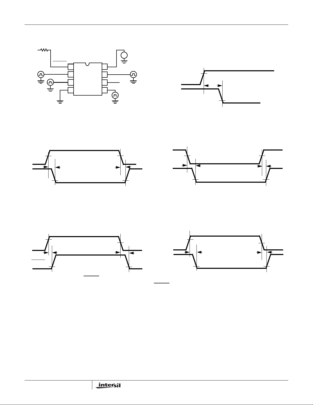
Test Circuit and Timing Diagrams
www.BDTIC.com/Intersil
R = 5K
5V
OV
V
UV
PWRGD
V
1
OV
2
ISL6140
UV
V
EE
ISL6150
3
4
FIGURE 1. TYPICAL TEST CIRCUIT FIGURE 2. SENSE TO GATE TIMING
8
7
6
5
V
DD
DRAIN
GATE
SENSE
ISL6140, ISL6150
+
48V
-
V
DRAIN
V
SENSE
SENSE
GATE
50mV
t
PHLSENSE
1V
2V
0V
13V
GATE
0V
OV
1.223V 1.203V
t
PHLOV
1V
FIGURE 3A. OV TO GATE TIMING FIGURE 3B. UV TO GATE TIMING
DRAIN
PWRGD
1.8V
t
1.0V
PLHPG
FIGURE 4A. DRAIN TO PWRGD
2V
1.223V 1.243V
t
PHLUV
1V
t
PLHUV
1V
t
PLHOV
1V
UV
0V
13V
GATE
0V
FIGURE 3. OV AND UV TO GATE TIMING
1.8V
1.0V
t
PLHPG
t
PHLPG
1.4V
1.0V
t
PHLPG
1.4V
DRAIN
PWRGD
1.0V
TIMING (ISL6140) FIGURE 4B. DRAIN TO PWRGD TIMING (ISL6150)
FIGURE 4. DRAIN TO PWRGD
/PWRGD TIMING
5
Page 6
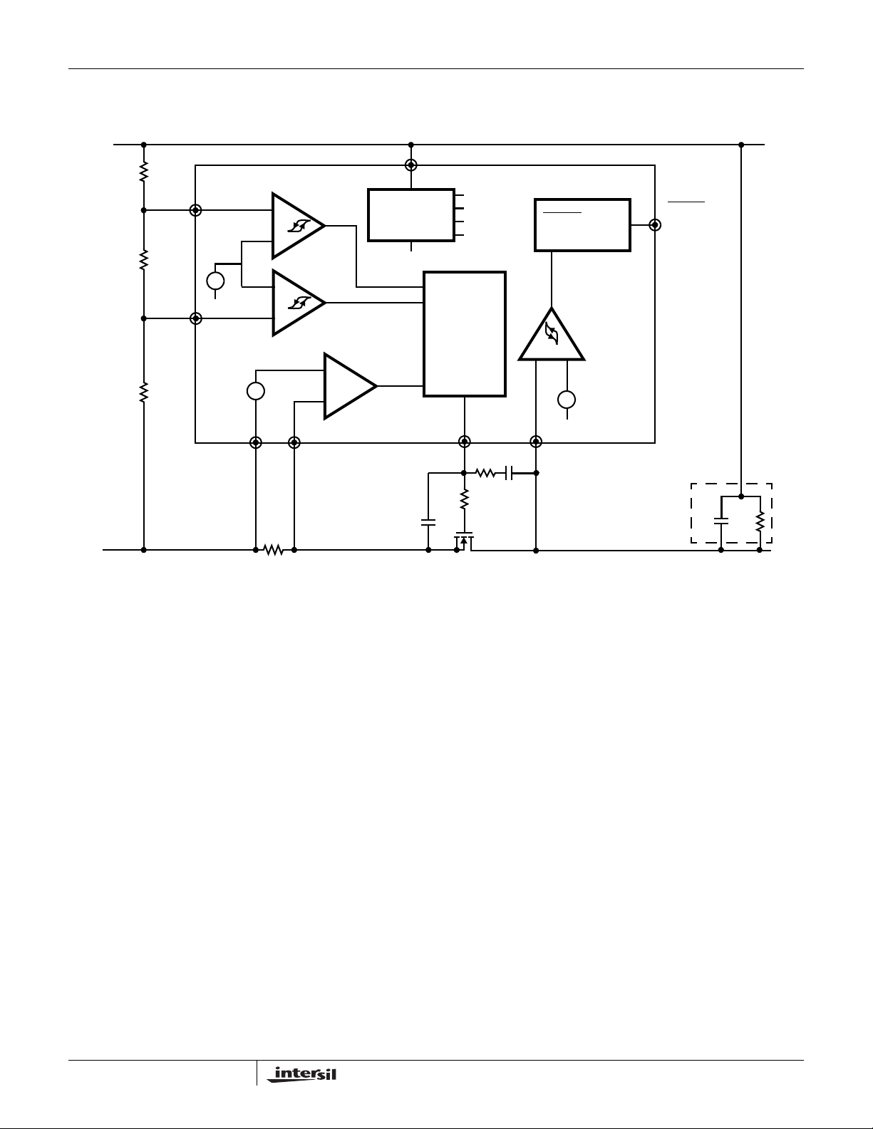
ISL6140/ISL6150 Block Diagram
www.BDTIC.com/Intersil
ISL6140, ISL6150
GND
R4
R5
R6
3 UV
2 OV
, V
V
UVL
(1.223V)
+
V
EE
EE
OVH
GND
8 V
DD
V
(INTERNAL
CC
-
+
VOLTAGE) AND
REFERENCE
GENERATOR
V
EE
C1
-
+
-
+
(50mV)
V
CB
+
V
EE
V
CC
VPG (1.7V)
V
UVL
VCB (50mV)
LOGIC AND
GATE DRIVE
R2
, V
OVH
C2R3
PWRGD/PWRGD
OUTPUT DRIVE
-
+
VPG (1.7V)
+
V
EE
7 DRAIN6 GATE5 SENSE4 V
1 PWRGD (6150)
1 PWRGD (6140)
CL
LOAD
RL
-48V IN
R1
Typical Values for a representative system; which
assumes:
36V to 72V supply range; 48 nominal; UV = 37V; OV = 71V
1A of typical current draw; 2.5 Amp Over-Current
100µF of load capacitance (CL); equivalent RL of 48Ω
(R = V/I = 48V/1A)
R1: 0.02Ω (1%)
R2: 10Ω (5%)
R3: 18kΩ (5%)
R4: 562kΩ (1%)
R5: 9.09kΩ (1%)
R6: 10kΩ (1%)
C1: 150nF (25V)
C2: 3.3nF (100V)
Q1: IRF530 (100V, 17A, 0.11Ω)
Q1
-48V OUT
Applications: Quick Guide to Choosing
Component Values
(See Block Diagram for reference)
This section will describe the minimum components needed
for a typical application, and will show how to select
component values. (Note that “typical” values may only be
good for this application; the user may have to select some
component values to match the system). Each block will
then have more detailed explanation of how it works, and
alternatives.
R4, R5, R6 - together set the Under-Voltage (UV) and OverVoltage (OV) trip points. When the power supply ramps up
and down, these trip points (and their 20mV nominal
hysteresis) will determine when the gate is allowed to turn on
and off (the UV and OV do not affect the PWRGD output).
The input power supply is divided down such that when each
pin is equal to the trip point (nominal is 1.223V), the
comparator will switch.
V
= 1.223 (R4 + R5 + R6)/(R5 + R6)
UV
V
= 1.223 (R4 + R5 + R6)/(R6)
OV
The values of R4 = 562K, R5 = 9.09K, and R6 = 10K will
give trip points of UV = 37V and OV = 71V.
6
Page 7

ISL6140, ISL6150
www.BDTIC.com/Intersil
Q1 - is the FET that connects the input supply voltage to the
output load, when properly enabled. It needs to be selected
based on several criteria: maximum voltage expected on the
input supply (including transients) as well as transients on
the output side; maximum current expected; power
dissipation and/or safe-operating-area considerations (due
to the quick over-current latch, power dissipation is usually
not a problem compared to systems where current limiting is
used; however, worst case power is usually at a level just
below the overcurrent shutdown). Other considerations
include the gate voltage threshold which affects the r
(which in turn, affects the voltage drop across the FET during
normal operation), and the maximum gate voltage allowed
(the IC clamp output is clamped to ~14V).
R1 - is the Over-Current sense resistor; if the input current is
high enough, such that the voltage drop across R1 exceeds
the SENSE comparator trip point (50mV nominal), the GATE
pin will go low, turning off the FET, to protect the load from
the excessive current. A typical value for R1 is 0.02Ω; this
sets an Over-Current trip point of I = V/R = 0.05/0.02 = 2.5A.
So, to choose R1, the user must first determine at what level
of current it should trip. Take into account worst case
variations for the trip point (50mV ±10mV = ±20%), and the
R1 resistance (typically 1% or 5%). Note that under normal
conditions, there will be a voltage drop across the resistor
(V = IR), so the higher the resistor value, the bigger the
voltage drop. Also note that the Over-Current should be set
above the inrush current level (plus the load current);
otherwise, it will latch off during that time (the alternative is to
lower the inrush current further). One rule of thumb is to set
the Over-Current 2-3 times higher than the normal current.
R1 = V / I
CL - is the sum of all load capacitances, including the load’s
input capacitance itself. Its value is usually determined by
the needs of the load circuitry, and not the hot plug (although
there can be interaction). For example, if the load is a
regulator, then the capacitance may be chosen based on the
input requirements of that circuit (holding regulation under
current spikes or loading, filtering noise, etc.) The value
chosen will then affect how the inrush current is controlled.
Note that in the case of a regulator, there may be capacitors
on the output of that circuit as well; these need to be added
into the capacitance calculation during inrush (unless the
regulator is delayed from operation by the PWRGD signal,
for example).
RL - is the equivalent resistive value of the load; it
determines the normal operation current delivered through
the FET. It also affects some dynamic conditions (such as
the discharge time of the load capacitors during a powerdown). A typical value might be 48Ω (I = V/R = 48/48 = 1A).
R2, C1, R3, C2 - are related to the gate driver, as it controls
the inrush current.
= 0.05V / Ioc (typical = 0.02Ω)
oc
DS(ON)
R2 prevents high frequency oscillations; 10Ω is a typical
value. R2 = 10Ω.
R3 and C2 act as a feedback network to control the inrush
current. I inrush = (Igate * CL)/C2, where CL is the load
capacitance (including module input capacitance), and Igate
is the gate pin charging current, nominally 45µA. So choose
a value of acceptable inrush for the system, and then solve
for C2. So I = 45µA * (CL/C2). Or C2 = (45µA * CL)/I.
C1 and R3 prevent Q1 from turning on momentarily when
power is first applied. Without them, C2 would pull the gate
of Q1 up to a voltage roughly equal to VEE*C2/Cgs(Q1)
(where Cgs is the FET gate-source capacitance) before the
ISL6140 could power up and actively pull the gate low. Place
C1 in parallel with the gate capacitance of Q1; isolate them
from C2 by R3.
C1 = (Vinmax - Vth)/Vth * (C2+Cgd) - where Vth is the
FET’s minimum gate threshold, Vinmax is the maximum
operating input voltage, and Cgd is the FET gate-drain
capacitance.
R3 = (Vinmax + deltaVgate)/5mA - its value is not critical; a
typical value is 18kΩ.
Applications: Inrush Current
The primary function of the ISL6140 hot plug controller is to
control the inrush current. When a board is plugged into a
live backplane, the input capacitors of the board’s power
supply circuit can produce large current transients as they
charge up. This can cause glitches on the system power
supply (which can affect other boards!), as well as possibly
cause some permanent damage to the power supply.
The key to allowing boards to be inserted into a live
backplane then is to turn on the power to the board in a
controlled manner, usually by limiting the current allowed to
flow through a FET switch, until the input capacitors are fully
charged. At that point, the FET is fully on, for the smallest
voltage drop across it.
In addition to controlling the inrush current, the ISL6140 also
protects the board against over-current, over-voltage, undervoltage, and can signal when the output voltage is within its
expected range (PWRGD).
Note that although this IC was designed for -48V systems, it
can also be used as a low-side switch for positive 48V
systems; the operation and components are usually similar.
One possible difference is the kind of level shifting that may
be needed to interface logic signals to the UV input (to reset
the latch) or PWRGD output. For example, many of the IC
functions are referenced to the IC substrate, connected to
the VEE pin. But this pin may be considered -48V or GND,
depending upon the polarity of the system. And input or
output logic (running at 5V or 3.3V or even lower) might be
externally referenced to either VDD or VEE of the IC, instead
of GND.
7
Page 8
ISL6140, ISL6150
www.BDTIC.com/Intersil
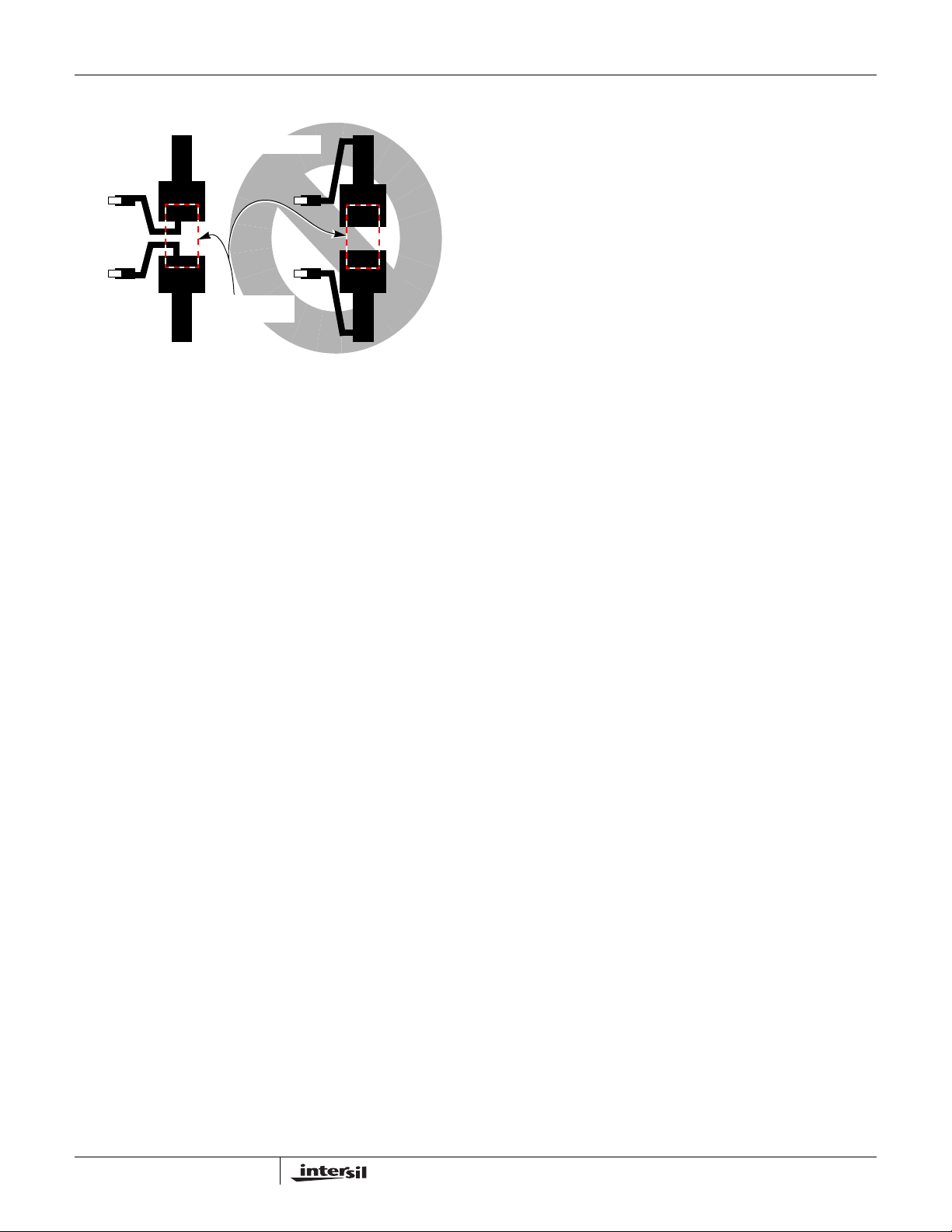
Applications: Over-Current
CORRECT
TO SENSE
AND V
EE
SENSE RESISTOR
FIGURE 5. SENSE RESISTOR
Physical layout of R1 SENSE resistor is critical to avoid
the possibility of false overcurrent occurrences. Since it is in
the main input-to-output path, the traces should be wide
enough to support both the normal current, and up to the
over-current trip point. Ideally trace routing between the R1
resistor and the ISL6140/ISL6150 (pin 4 (VEE) and pin 5
(SENSE) is direct and as short as possible with zero current
in the sense lines. (See Figure 5).
There is a short filter (3µs nominal) on the comparator; current
spikes shorter than this will be ignored. Any longer pulse will
shut down the output, requiring the user to either power down
the system (below the UV voltage), or pull the UV pin below its
trip point (usually with an external transistor).
If current pulses longer than the 3µs are expected, and need
to be filtered, then an additional resistor and capacitor can
be added. As shown in Figure 29, R7 and C3 act as a lowpass filter such that the voltage on the SENSE pin won’t rise
as fast, effectively delaying the shut-down. Since the
ISL6140/ISL6150 has essentially zero current on the
SENSE pin, there is no voltage drop or error associated with
the extra resistor. R7 is recommended to be small, 100Ω is a
good value.
The delay time is approximated by the added RC time
constant, modified by a factor relative to the trip point.
t = - R * C * ln [1 - (V(t) - V(t
where V(t) is the trip voltage (nominally 50mV); V(t0) is the
nominal voltage drop across the sense resistor before the
over-current condition; V
sense resistor while the over-current is applied.
For example: a system has a normal 1A current load, and a
20mΩ sense resistor, for a 2.5A over-current. It needs to
filter out a 50µs current pulse at 5A. So,
V(t) = 50mV (from spec)
V(t
) = 20mV (V = IR = 1A * 20mΩ)
0
= 100mV (V = IR = 5A * 20mΩ)
V
i
If R7 = 100Ω, then C3 is around 1µF.
INCORRECT
CURRENT
)) / (Vi - V(t0))]
0
is the voltage drop across the
i
Note that the FET must be rated to handle the higher current
for the longer time, since the IC is not doing current limiting;
the RC is just delaying the over-current shutdown.
Applications: OV and UV
The UV and OV input pins are high impedance, so the value
of the external resistor divider is not critical with respect to
input current. Therefore, the next consideration is total
current; the resistors will always draw current, equal to the
supply voltage divided by the total of R4+R5+R6; so the
values should be chosen high enough to get an acceptable
current. However, to the extent that the noise on the power
supply can be transmitted to the pins, the resistor values
might be chosen to be lower. A filter capacitor from UV to
VEE or OV to UV is a possibility, if certain transients need to
be filtered. (Note that even some transients which will
momentarily shut off the gate might recover fast enough
such that the gate or the output current does not even see
the interruption).
Finally, take into account whether the resistor values are
readily available, or need to be custom ordered. Tolerances
of 1% are recommended for accuracy. Note that for a typical
48V system (with a 36V to 72V range), the 36V or 72V is
being divided down to 1.223V, a significant scaling factor.
For UV, the ratio is roughly 30 times; every 3mV change on
the UV pin represents roughly 0.1V change of power supply
voltage. Conversely, an error of 3mV (due to the resistors,
for example) results in an error of 0.1V for the supply trip
point. The OV ratio is around 60. So the accuracy of the
resistors comes into play.
The hysteresis of the comparators (20mV nominal) is also
multiplied by the scale factor of 30 for the UV pin
(30 * 20mV = 0.6V of hysteresis at the power supply) and 60
for the OV pin (60 * 20mV = 1.2V of hysteresis at the power
supply).
With the three resistors, the UV equation is based on the
simple resistor divider:
1.223 = V
V
= 1.223 (R4 + R5 + R6)/(R5 + R6)
UV
Similarly, for OV:
1.223 = V
VOV = 1.223 (R4 + R5 + R6)/(R6)
Note that there are two equations, but 3 unknowns. Because
of the scale factor, R4 has to be much bigger than the other
two; chose its value first, to set the current (for example,
50V/500kΩ draws 100µA), and then the other two will be in
the 10kΩ range. Solve the two equations for two unknowns.
Note that some iteration may be necessary to select values
that meet the requirement, and are also readily available
standard values.
* (R5 + R6)/(R4 + R5 + R6) or
UV
* (R6)/(R4 + R5 + R6) or
OV
8
Page 9

ISL6140, ISL6150
www.BDTIC.com/Intersil
The three resistors (R4, R5, R6) is the recommended
approach for most cases. But if acceptable values can’t be
found, then consider 2 separate resistor dividers (one for
each pin; both from VDD to VEE). This also allows the user
to adjust or trim either trip point independently.
Note that the top of the resistor dividers is shown in Figure
29 as GND (Short pin). In a system where cards are plugged
into a backplane (or any other case where pins are plugged
into an edge connector) the user may want to take
advantage of the order in which pins make contact. Typically,
pins on either end of the card make contact first (although
you may not know which end is first). If you combine that
with designating a pin near the center as the short pin GND,
and make it shorter than the rest, then it should be the last
pin to make contact.
The advantage of doing this: the VDD and VEE pin
connections are made first. The IC is powered up, but since
the top of the resistor divider is still open, both the UV and
OV pins are pulled low to VEE, which will keep the gate off.
This allows the IC time to get initialized, and also allows the
power supply to charge up any input capacitance. By the
time the resistor divider makes contact, the power supply
voltage on the card is presumably stabilized, and the IC
ready to respond; when the UV pin reaches the proper
voltage, the IC will turn on the GATE of the FET, and starts
the controlled inrush current charging.
Note that this is not a requirement; if the IC gets powered at
the same time as the rest of the board, it should be able to
properly control the inrush current. But if finer control is
needed, there are many variables involved to consider: the
number of pins in the connector; the lengths of the pins; the
amount of mechanical play in the pin-to-connector interface;
the amount of extra time versus the shorter pin length; the
amount of input capacitance versus the ability of the power
supply to charge it; the manufacturing cost adder (if any) of
different length pins; etc.
ISL6140 (L version; Figure 6): Under normal conditions
(DRAIN < VPG), the Q2 DMOS will turn on, pulling PWRGD
low, enabling the module.
VDD
(SECTION OF) ISL6140
(L VERSION)
VPG (1.7V)
+
-
+
-
FIGURE 6. ACTIVE LOW ENABLE MODULE
Q2
VEE
PWRGD
CL
DRAIN
+
VIN+
VOUT+
/OFF
ON
ACTIVE LOW
ENABLE
MODULE
VIN-
VOUT-
When the DRAIN is too high, the Q2 DMOS will shut off
(high impedance), and the pin will be pulled high by the
external module (or an optional pull-up resistor or
equivalent), disabling the module. If a pull-up resistor is
used, it can be connected to any supply voltage that doesn’t
exceed the IC pin maximum ratings on the high end, but is
high enough to give acceptable logic levels to whatever
signal it is driving. An external clamp may be used to limit the
range.
VDD
(SECTION OF) ISL6140
(L VERSION)
VPG
(1.7V)
+
+
-
-
FIGURE 7. ACTIVE LOW ENABLE OPTO-ISOLATOR
Q2
VEE
PWRGD
DRAIN
R12
OPTO
PWRGD
Applications: PWRGD/PWRGD
The PWRGD/PWRGD outputs are typically used to directly
enable a power module, such as a DC/DC converter. The
PWRGD
enable (L version); PWRGD (ISL6150) for those with active
(ISL6140) is used for modules with active low
The PWRGD
can also drive an opto-coupler (such as a
4N25), as shown in Figure 7 or LED (Figure 8). In both
cases, they are on (active) when power is good. Resistors
R12 or R13 are chosen, based on the supply voltage, and
the amount of current needed by the loads.
high enable (H version). The modules usually have a pull-up
device built-in, as well as an internal clamp. If not, an
external pull-up resistor may be needed, since the output is
open drain. If the pin is not used, it can be left open.
For both versions, the PG comparator compares the DRAIN
pin to VEE (connected to the source of the FET); if the
voltage drop exceeds VPG (1.7V nominal), that implies the
(SECTION OF) ISL6140
(L VERSION)
VPG
(1.7V)
+
-
+
-
drop across the FET is too high, and the PWRGD pin should
go in-active (power-NO-GOOD).
FIGURE 8. ACTIVE LOW ENABLE WITH LED
9
VDD
R13
PWRGD
LED (GREEN)
Q2
VEE
DRAIN
Page 10

ISL6140, ISL6150
www.BDTIC.com/Intersil
ISL6150 (H version; Figure 9): Under normal conditions
(DRAIN < VPG), the Q3 DMOS will be on, shorting the
bottom of the internal resistor to VEE, and turning Q2 off. If
the pull-up current from the external module is high enough,
the voltage drop across the 6.2kΩ resistor will look like a
logic high (relative to DRAIN). Note that the module is only
referenced to DRAIN, not VEE (but under normal conditions,
the FET is on, and the DRAIN and VEE are almost the same
voltage).
When the DRAIN voltage is high compared to VPG, Q3
DMOS turns off, and the resistor and Q2 clamp the PWRGD
pin to one diode drop (~0.7V) above the DRAIN pin. This
should be able to pull low against the module pull-up current,
and disable the module.
VDD
(SECTION OF) ISL6150
(H VERSION)
VPG
(1.7V)
+
-
+
-
FIGURE 9. ACTIVE HIGH ENABLE MODULE
RPG
6.2K
Q3
VEE
PWRGD
Q2
DRAIN
CL
+
VIN+
VOUT+
ON/OFF
ACTIVE HIGH
ENABLE
MODULE
VIN-
VOUT-
Applications: GATE pin
To help protect the external FET, the output of the GATE pin
is internally clamped; up to an 80V supply, it will not be any
higher than 15V (nominal 14V). From about 18V down to
10V, the GATE voltage will be around 4V below the supply
voltage; at 10V supply, the minimum GATE voltage is 5.4V
(worst case is at -40°C).
Applications: Optional Components
In addition to the typical application, and the variations
already mentioned, there are a few other possible
components that might be used in specific cases. See
Figure 29 for some possibilities.
If the input power supply exceeds the 100V absolute
maximum rating, even for a short transient, that could cause
permanent damage to the IC, as well as other components
on the board. If this cannot be guaranteed, a voltage
suppressor (such as the SMAT70A, D1) is recommended.
When placed from VDD to VEE on the board, it will clamp
the voltage.
If transients on the input power supply occur when the
supply is near either the OV or UV trip points, the GATE
could turn on or off momentarily. One possible solution is to
add a filter cap C4 to the VDD pin, through isolation resistor
R10. A large value of R10 is better for the filtering, but be
aware of the voltage drop across it. For example, a 1kΩ
resistor, with 1mA of IDD would have 1V across it and
dissipate 1mW. Since the UV and OV comparators are
referenced with respect to the VEE supply, they should not
be affected. But the GATE clamp voltage could be offset by
the voltage across the extra resistor.
If there are negative transients on the DRAIN pin, blocking
diodes may help limit the amount of current injected into the
IC substrate. General purpose diodes (such as 1N4148)
may be used. Note that the ISL6140 (L version) requires one
diode, while the ISL6150 (H version) requires two diodes.
One consequence of the added diodes it that the V
PG
voltage is offset by each diode drop.
The switch SW1 is shown as a simple pushbutton. It can be
replaced by an active switch, such as an NPN or NFET; the
principle is the same; pull the UV node below its trip point,
and then release it (toggle low). To connect an NFET, for
example, the drain goes to UV; the source to VEE, and the
gate is the input; if it goes high (relative to VEE), it turns the
NFET on, and UV is pulled low. Just make sure the NFET
resistance is low compared to the resistor divider, so that it
has no problem pulling down against it.
R8 is a pull-up resistor for PWRGD
, if there is no other
component acting as a pull-up device. The value of R8 is
determined by how much current you want when pulled low
(also affected by the VDD voltage); and you want to pull it
low enough for a good logic low level. An LED can also be
placed in series with R8, if desired. In that case, the criteria
is the LED brightness versus current.
R7 and C3 are used to delay the Over-Current shutdown, as
described in the OV and UV section.
Applications: “Brick” Regulators
One of the typical loads used are DC/DC regulators, some
commonly known as “brick” regulators, (partly due to their
shape, and because it can be considered a “building block”
of a system). For a given input voltage range, there are
usually whole families of different output voltages and
current ranges. There are also various standardized sizes
and pinouts, starting with the original “full” brick, and since
getting smaller (half-bricks and quarter-bricks are now
common).
Other common features may include: all components
(except some filter capacitors) are self-contained in a
molded plastic package; external pins for connections; and
often an ENABLE input pin to turn it on or off. A hot plug IC,
such as the ISL6140, is often used to gate power to a brick,
as well as turn it on.
Many bricks have both logic polarities available (Enable Hi or
Lo input); select the ISL6140 (L version) and ISL6150 (H
version) to match. There is little difference between them,
although the L version output is usually simpler to interface.
The Enable input often has a pull-up resistor or current
source, or equivalent built in; care must be taken in the
10
Page 11

ISL6140, ISL6150
www.BDTIC.com/Intersil
ISL6150 (H version) output that the given current will create
a high enough input voltage (remember that current through
the RPG 6.2kΩ resistor generates the high voltage level; see
Figure 9).
The input capacitance of the brick is chosen to match its
system requirements, such as filtering noise, and
maintaining regulation under varying loads. Note that this
input capacitance appears as the load capacitance of the
ISL6140/ISL6150.
The brick’s output capacitance is also determined by the
system, including load regulation considerations. However, it
can affect the ISL6140/ISL6150, depending upon how it is
enabled. For example, if the PWRGD signal is not used to
enable the brick, the following could occur. Sometime during
the inrush current time, as the main power supply starts
charging the brick input capacitors, the brick itself will start
working, and start charging its output capacitors and load;
that current has to be added to the inrush current. In some
cases, the sum could exceed the Over-Current shutdown,
which would shut down the whole system! Therefore,
whenever practical, it is advantageous to use the PWRGD
output to keep the brick off at least until the input caps are
charged up, and then start-up the brick to charge its output
caps.
Applications: Layout Considerations
For the minimum application, there are only 6 resistors, 2
capacitors, one IC and one FET. A sample layout is shown in
Figure 30. It assumes the IC is 8-SOIC; the FET is in a
D2PAK (or similar SMD-220 package).
Although GND planes are common with multi-level PCBs, for
a -48V system, the -48V rails (both input and output) act
more like a GND than the top 0V rail (mainly because the IC
signals are mostly referenced to the lower rail). So if
separate planes for each voltage are not an option, consider
prioritizing the bottom rails first.
Note that with the placement shown, most of the signal lines
are short, and there should not be much interaction between
them.
Although decoupling capacitors across the IC supply pins
are often recommended in general, this application may not
need one, nor even tolerate one. For one thing, a decoupling
cap would add to (or be swamped out by) any other input
capacitance; it also needs to be charged up when power is
applied. But more importantly, there are no high speed (or
any) input signals to the IC that need to be conditioned. If still
desired, consider the isolation resistor R10, as shown in
Figure 29.
Typical brick regulators include models such as Lucent
JW050A1-E or Vicor VI-J30-CY. These are nominal -48V
input, and 5V outputs, with some isolation between the input
and output.
11
Page 12

Typical Performance Curves
www.BDTIC.com/Intersil
ISL6140, ISL6150
1.000
0.800
0.600
0.400
IDD CURRENT (mA)
0.200
0.000
0 20406080100
VDD VOLTAGE (V)
FIGURE 10. IDD vs VDD FIGURE 11. VGATE vs VDD
1.000
0.800
0.600
15.000
12.000
9.000
6.000
VGATE (V)
3.000
0.000
0 20406080100
VDD (V)
15.000
12.000
9.000
0.400
IDD CURRENT (mA)
0.200
0.000
0481216202 6 10 14 18
VDD VOLTAGE (V)
6.000
VGATE (V)
3.000
0.000
0481216202 6 10 14 18
VDD (V)
FIGURE 12. IDD vs VDD (<20V) FIGURE 13. VGATE vs VDD (<20V)
0.95
0.93
0.91
0.89
CURRENT (mA)
0.87
0.85
-40 10 60 110
TEMPERATURE (°C)
14.5
14.3
14.1
13.9
GATE VOLTAGE (V)
13.7
13.5
-40 10 60 110
TEMPERATURE (°C)
FIGURE 14. IDD CURRENT (AT VDD = 80V) FIGURE 15. GATE VOLTAGE (AT VDD = 80V)
12
Page 13

Typical Performance Curves (Continued)
www.BDTIC.com/Intersil
ISL6140, ISL6150
14.5
14.0
13.5
13.0
GATE VOLTAGE (V)
12.5
12.0
-40 10 60 110
TEMPERATURE (°C)
7.5
7.0
6.5
6.0
GATE VOLTAGE (V)
5.5
5.0
-40 10 60 110
TEMPERATURE (°C)
FIGURE 16. GATE VOLTAGE (AT VDD = 17V) FIGURE 17. GATE VOLTAGE (AT VDD = 10V)
-0.048
-0.050
-0.052
45
40
35
-0.054
CURRENT (mA)
-0.056
-0.058
-40 10 60 110
TEMPERATURE (°C)
FIGURE 18. GATE PULL-UP CURRENT FIGURE 19. GATE PULL-DOWN CURRENT
0.34
0.32
0.3
0.28
VOLTAGE (V)
0.26
0.24
-40 10 60 110
TEMPERATURE (°C)
FIGURE 20. PWRGD
(ISL6140) VOL (AT 1mA) VOLTAGE FIGURE 21. PWRGD (ISL6150) IMPEDANCE (kΩ)
30
CURRENT (mA)
25
20
-40 10 60 110
TEMPERATURE (°C)
7.5
7.0
6.5
6.0
IMPEDANCE (kΩ)
5.5
5.0
-40 10 60 110
TEMPERATURE (°C)
13
Page 14

Typical Performance Curves (Continued)
www.BDTIC.com/Intersil
ISL6140, ISL6150
1.90
1.85
1.80
1.75
TRIP VOLTAGE (V)
1.70
1.65
-40 10 60 110
TEMPERATURE (°C)
1.35
1.3
1.25
1.2
TRIP VOLTAGE (V)
1.15
1.1
-40 10 60 110
TEMPERATURE (°C)
FIGURE 22. DRAIN/PG UP TRIP VOLTAGE FIGURE 23. DRAIN/PG DOWN TRIP VOLTAGE
0.55
0.53
0.51
0.0550
0.0530
0.0510
0.49
VOLTAGE (V)
0.47
0.45
-40 10 60 110
TEMPERATURE (°C)
0.0490
TRIP VOLTAGE (V)
0.0470
0.0450
-40 10 60 110
TEMPERATURE (°C)
FIGURE 24. DRAIN/PG HYSTERESIS VOLTAGE FIGURE 25. SENSE TRIP VOLTAGE
14
Page 15

Inrush Current
m
ISL6140, ISL6150
www.BDTIC.com/Intersil
Inrush Current
In the example in Figure 26, the supply voltage is 48V and
the load resistor (RL) is 620Ω, for around 80mA. The load
capacitance is 100µF (100V). The Sense Resistor (R1) is
0.02Ω (trip point at 2.5A; well above the inrush current here).
Note that the load current starts at 0 (FET off); reaches a
peak of ~850mA as the GATE voltage ramps and turns on
the FET slowly, and then settles out at 80mA, once the CL is
fully charged to the 48V. The width of the inrush current
pulse is 8ms wide. For comparison, with the same
conditions, but without the gate-controlled FET, the current
was over 20A, during a 130µs pulse.
Load
Current
48V
GATE
PWRGD-bar
FIGURE 26. INRUSH CURRENT
Power Supply Ramp
Figure 27 shows the Power Supply voltage (to the VDD pin,
with respect to GND at the VEE pin) ramping up. In this
case, the values chosen were R4 = 562K; R5 = 5.9K;
R6 = 13.3K; that sets the UV trip point around 38V, and the
OV trip point to 54V. Note that the GATE starts at 0V, and
stays there until the UV trip point (38V) is exceeded; then it
ramps (slowly, based on the external components chosen)
up to around 13V, where it is clamped; it stays there until the
power supply exceeds the OV trip point at 54V (the GATE
shut-off is much faster than the turn-on). The total time scale
is 2 seconds; the VDD ramp speed was simply based on the
inherent characteristic of the particular power supply used.
FIGURE 27. POWER SUPPLY RAMP
Over-Current at 2.3A
In Figure 28, an Electronic Load Generator was used to
ramp the load current; no load resistor or capacitor was
connected. The sense Resistor R1 is 0.02Ω; that should
make the nominal Over-Current trip point 2.5A.
The GATE is high (clamped to around 13V), keeping the
FET on, as the current starts to ramp up from zero; the
GATE starts to go low (to shut off the FET) when the load
current hits 2.3A. Note that it takes only 44µs for the GATE
to shut off the FET (when the load current equals zero).
Keep in mind that the tolerance of the sense resistor (1%
here) and the IC Over-Current trip voltage (V
accuracy of the trip point; that’s why the trip point doesn’t
necessarily equal the 2.5A design target.
Load Current
2.3 A
) affect the
CB
R1 = 0.02 oh
48V
No cap
GATE
Ω
FIGURE 28. OVER-CURRENT AT 2.3A
FIGURE 28. OVER-CURRENT AT 2.3A
15
Page 16

ISL6140, ISL6150
www.BDTIC.com/Intersil
GND GND
GND
(SHORT PIN)
G
NFET*
(INSTEAD
OF SW1)
-V IN -V OUT
C4*
R11
SW1
D1*
R12
R4
UV
OV
R5
FIGURE 29. ISL6140/50 OPTIONAL COMPONENTS (SHOWN WITH *)
R6*
R10*
V
DD
ISL6140 (L)
V
SENSE GATE DRAIN
EE
C3*
R7*
C1
R1
Q1
R2
R3
PWRGD
D2*
C2
D3*
R8*
Optional Components (see text for when they should be used)
D1 is a voltage suppressor; SMAT70A or equivalent.
D2 and D3 are DRAIN diodes; the ISL6150 (H version) uses
both D2 and D3; the ISL6140 (L version) uses just D2. If
neither is used, short the path of either, to connect the
DRAIN pin to C2 and Q1. The 1N4148 is a typical diode.
R6 is used to add more hysteresis to the UV threshold,
which already has a built-in 20mV hysteresis. With R6, the
new thresholds with a rising and falling input are:
R5 R6 R4 R6 R4 R5•+•+•
Vuv rising()VUVH
-------------------------------------------------------------- ----------------
•=
R5 R6•
CL*
SW1 is a push-button switch, that can manually reset the
fault latch after an Over-Current shutdown. It can also be
replaced by a transistor switch.
R10 and C4 are used to filter the VDD voltage, such that
small transients on the input supply do not trigger UV or OV.
R7 and C3 are used to delay the Over-Current shutdown. R7
should be shorted, if not used. See the Over-Current section
for more details.
R8 is a pull-up resistor for PWRGD
, if there is no other
component acting as a pull-up device. An LED can also be
placed in series with R8, if desired. See Figure 8.
CL is any extra output Load capacitance, which can also be
considered input capacitance for the external module.
16
R5 R6 R4 R6 R4 R5•+•+•
Vuv falling()VUVL
--------------------------------------------------------------- ---------------
• Vgate
R5 R6•
•–=
Since R6 is connected directly to the GATE output, it will
reduce the available gate current, which will reduce the dv/dt
across the MOSFET and hence the inrush current. The
value of R6 should be kept as high as possible (greater than
500K recommended) so that it does not drag down the
GATE voltage below the value required to ensure the
MOSFET is fully enhanced.
R4
--------
R6
Page 17

ISL6140, ISL6150
www.BDTIC.com/Intersil
GND GND
C2
VDD 8
D 7
G 6
S 5
-48V IN
R6
R5
R4
1 PG
2 OV
3 UV
4 VEE
U1
R1
FIGURE 30. SAMPLE LAYOUT (NOT TO SCALE)
Figure 30 shows a sample component placement and
routing for the typical application shown in Figure 31.
GND GND
R4
R5
R6
-48V IN
UV
OV
V
EE
FIGURE 31. TYPICAL APPLICATION
V
DD
R3
PWRGD
C2
ISL6140
SENSE GATE DRAIN
C1
R2
R1
Q1
(LOAD)
RL
-48V OUT
CL
R3
R2
C1
G
DRAIN
FET
S
-48V OUT
NOTES:
1. Layout scale is approximate; routing lines are just for illustration
purposes; they do not necessarily conform to normal PCB
design rules. High current buses are wider, shown with parallel
lines.
2. Approximate size of the above layout is 1.6 x 0.6 inches; almost
half of the area is just the FET (D2PAK or similar SMD-220
package).
3. R1 sense resistor is size 2512; all other R’s and C’s shown are
0805; they can all potentially use smaller footprints, if desired.
4. The RL and CL are not shown on the layout.
5. R4 uses a via to connect to GND on the bottom of the board; all
other routing can be on top level. (It’s even possible to eliminate
the via, for an all top-level route).
6. PWRGD
signal is not used here.
7. BOM (Bill Of Materials)
R1 = 0.02Ω (5%)
R2 = 10Ω (5%)
R3 = 18kΩ (5%)
R4 = 562kΩ (1%)
R5 = 9.09kΩ (1%)
R6 = 10kΩ (1%)
C1 = 150nF (25V)
C2 = 3.3nF (100V)
Q1 = IRF530 (100V, 17A, 0.11Ω)
17
Page 18

ISL6140, ISL6150
www.BDTIC.com/Intersil
Small Outline Plastic Packages (SOIC)
N
INDEX
AREA
123
-AD
e
B
0.25(0.010) C AM BS
NOTES:
1. Symbols are defined in the “MO Series Symbol List” in Section 2.2 of
Publication Number 95.
2. Dimensioning and tolerancing per ANSI Y14.5M-1982.
3. Dimension “D” does not include mold flash, protrusions or gate burrs.
Mold flash, protrusion and gate burrs shall not exceed 0.15mm (0.006
inch) per side.
4. Dimension “E” does not include interlead flash or protrusions. Interlead flash and protrusions shall not exceed 0.25mm (0.010 inch) per
side.
5. The chamfer on the body is optional. If it is not present, a visual index
feature must be located within the crosshatched area.
6. “L” is the length of terminal for soldering to a substrate.
7. “N” is the number of terminal positions.
8. Terminal numbers are shown for reference only.
9. The lead width “B”, as measured 0.36mm (0.014 inch) or greater
above the seating plane, shall not exceed a maximum value of
0.61mm (0.024 inch).
10. Controlling dimension: MILLIMETER. Converted inch dimensions
are not necessarily exact.
E
-B-
SEATING PLANE
A
-C-
M
0.25(0.010) BM M
H
α
µ
A1
0.10(0.004)
L
h x 45
o
C
M8.15 (JEDEC MS-012-AA ISSUE C)
8 LEAD NARROW BODY SMALL OUTLINE PLASTIC
PACKAGE
INCHES MILLIMETERS
SYMBOL
A 0.0532 0.0688 1.35 1.75 -
A1 0.0040 0.0098 0.10 0.25 -
B 0.013 0.020 0.33 0.51 9
C 0.0075 0.0098 0.19 0.25 D 0.1890 0.1968 4.80 5.00 3
E 0.1497 0.1574 3.80 4.00 4
e 0.050 BSC 1.27 BSC -
H 0.2284 0.2440 5.80 6.20 h 0.0099 0.0196 0.25 0.50 5
L 0.016 0.050 0.40 1.27 6
N8 87
o
α
0
o
8
o
0
o
8
Rev. 0 12/93
NOTESMIN MAX MIN MAX
-
All Intersil U.S. products are manufactured, assembled and tested utilizing ISO9000 quality systems.
Intersil Corporation’s quality certifications can be viewed at www.intersil.com/design/quality
Intersil products are sold by description only. Intersil Corporation reserves the right to make changes in circuit design, software and/or specifications at any time without
notice. Accordingly, the reader is cautioned to verify that data sheets are current before placing orders. Information furnished by Intersil is believed to be accurate and
reliable. However, no responsibility is assumed by Intersil or its subsidiaries for its use; nor for any infringements of patents or other rights of third parties which may result
from its use. No license is granted by implication or otherwise under any patent or patent rights of Intersil or its subsidiaries.
For information regarding Intersil Corporation and its products, see www.intersil.com
18
 Loading...