

Page 1
查询ISL6121HEVAL1供应商
®
ISL6123, ISL6124, ISL6125,
ISL6126, ISL6127, ISL6128
Data Sheet June 10, 2005
Power Sequencing Controllers
The Intersil ISL6123, ISL6124, ISL6125, ISL6126, ISL6127,
ISL6128 are integrated 4 channel controlled-on/controlledoff power-supply sequencers with supply monitoring, fault
protection and a “sequence completed” signal (RESET#).
For larger systems, more than 4 supplies can be sequenced
by simply connecting a wire between SYSRESET# pins of
cascaded IC's. The ISL6125 uses 4 open-drain outputs to
control the 4 power supplies, and the other sequencers use
a patented, micropower 7X chargepump to drive 4 external
low-cost NFET switch gates above the supply rail by 5.3V.
These IC's can be biased from any supply 5V down to 1.5V.
Individual product descriptions are below.
The four channel ISL6123 (ENABLE input), ISL6124
(ENABLE# input) and ISL6125 ICs offer the designer 4 rail
control when it is required that all four rails are in minimal
compliance prior to turn on and that compliance must be
maintained during operation. The ISL6123 has a low power
standby mode when it is disabled, suitable for battery
powered applications.
The ISL6125 operates like the ISL6124 but instead of
charge pump driven gate drive outputs it has open drain
logic outputs for direct interface to other circuitry.
In contrast to the ISL6123 and ISL6124, with the ISL6126,
each of the four channels operates independently so that the
various rails will turn on once its individual input voltage
requirements are met.
The ISL6127 is a preprogrammed A-B-C-D turn-on and D-CB-A turn-off sequenced IC. Once all inputs are in compliance
and ENABLE
subsequent GATE will turn-on after the previous one
completes turning-on.
The ISL6128 has two groups of two channels each with its
independent I/O and is ideal for voltage sequencing into
redundant capability loads as all four inputs need to be
satisfied prior to turn on but a single group fault is ignored by
the other group.
External resistors provide flexible voltage threshold
programming of monitored rail voltages. Delay and
sequencing are provided by external capacitors for both
ramp up and ramp down.
Additional I/O is provided indicating and driving RESET state
in various configurations.
For volume applications, other programmable options and
features can be had. Contact the factory with your needs.
is asserted the sequencing starts and each
FN9005.4
Features
• Enables arbitrary turn-on and turn-off sequencing of up to
four power supplies (0.7V - 5V)
• Operates from 1.5V to 5V supply voltage
• Supplies VDD +5.3V of charge pumped gate drive
• Adjustable voltage slew rate for each rail
• Multiple sequencers can be daisy-chained to sequence an
infinite number of independent supplies
• Glitch immunity
• Under voltage lockout for each supply
• 1µA Sleep State (ISL6123)
• Active high (ISL6123) or low (ISL6124) ENABLE# input
• Open drain version available (ISL6125)
• Pre programmed Sequence available (ISL6127)
• Dual channel groupings (ISL6128)
• QFN Package with Pb-free plus anneal option
Applications
• Graphics cards
• FPGA/ASIC/microprocessor/PowerPC supply sequencing
• Network routers
• Telecommunications systems
Ordering Information
TEMP.
PART NUMBER
ISL6123IR -40 to +85 24 Ld 4x4 QFN L24.4x4
ISL6124IR
ISL6125IR
ISL6126IR
ISL6127IR
ISL6128IR
ISL6123IRZA (Note) -40 to +85 24 Ld 4x4 QFN
ISL6124IRZA (Note)
ISL6125IRZA (Note)
ISL6126IRZA (Note)
ISL6127IRZA (Note)
ISL6128IRZA (Note)
ISL612XSEQEVAL1 Evaluation Platform
NOTE: Intersil Pb-free plus anneal products employ special Pb-free
material sets; molding compounds/die attach materials and 100% matte
tin plate termination finish, which are RoHS compliant and compatible
with both SnPb and Pb-free soldering operations. Intersil Pb-free
products are MSL classified at Pb-free peak reflow temperatures that
meet or exceed the Pb-free requirements of IPC/JEDEC J STD-020.
RANGE (°C) PACKAGE
(Pb-free)
PKG.
DWG. #
1
CAUTION: These devices are sensitive to electrostatic discharge; follow proper IC Handling Procedures.
1-888-INTERSIL or 1-888-468-3774
| Intersil (and design) is a registered trademark of Intersil Americas Inc.
Copyright Intersil Americas Inc.2001, 2003, 2004 All Rights Reserved.
All other trademarks mentioned are the property of their respective owners.
Page 2
ISL6123, ISL6124, ISL6125, ISL6126, ISL6127, ISL6128
Pinout
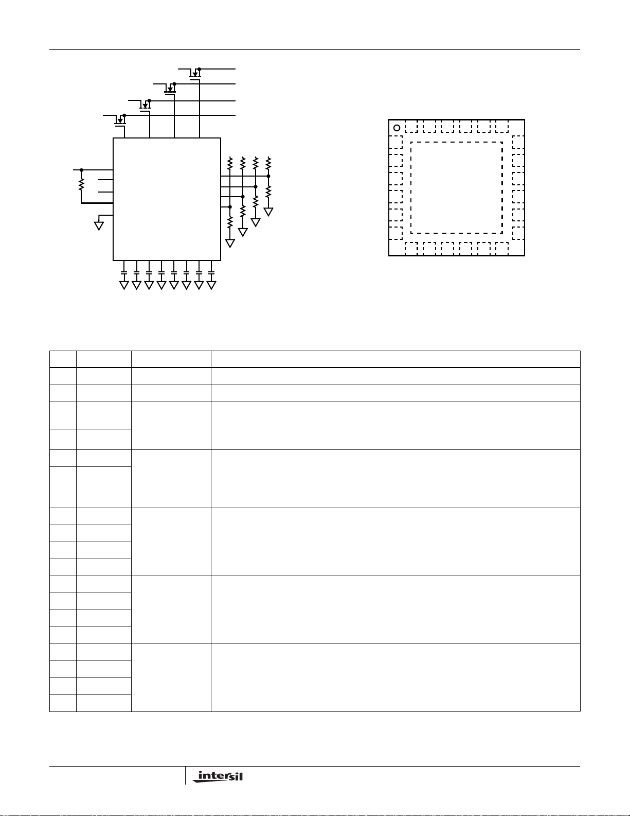
ISL6123, ISL6124, ISL6125,
ISL6126, ISL6127, ISL6128 (QFN)
TOP VIEW
24 23 22 21 20 19
1
2
3
4
5
6
789101112
4mm X 4mm
18
17
16
15
14
13
DIN
CIN
V
DD
ENABLE
SYSRST#
RESET#
GROUND
BIN
GATE D
DLY_ON_A
DLY_OFF_A
GATE C
DLY_OFF_B
DLY_ON_B
GATE B
DLY_OFF_C
DLY_ON_C
GATE A
UVLO_A
UVLO_B
UVLO_C
UVLO_D
DLY_ON_D
AOUTAIN
BOUT
COUT
DOUT
IN
A
BIN
CIN
DIN
DLY_OFF_D
FIGURE 1. TYPICAL ISL6123 APPLICATION USAGE
Pin Descriptions
PIN # PIN NAME FUNCTION DESCRIPTION
23 VDD Chip Bias Bias IC from nominal 1.5V to 5V
10 GND Bias Return IC ground
1 ENABLE_1/
ENABLE#_1
11 ENABLE#_2
24 RESET# RESET# Output RESET# provides a low signal 150ms after all GATEs are fully enhanced. This delay is for stabilization of
9 RESET#_2
20 UVLO_A Under Voltage Lock
12 UVLO_B
17 UVLO_C
14 UVLO_D
21 DLY_ON_A Gate On Delay
8DLY_ON_B
16 DLY_ON_C
15 DLY_ON_D
18 DLY_OFF_A Gate Off Delay
13 DLY_OFF_B
3 DLY_OFF_C
4 DLY_OFF_D
Input to start on/off
sequencing.
Out/Monitoring
Input
Timer Output
Timer Output
Input to initiate the start of the programmed sequencing of supplies on or off. Enable functionality is
disabled for 10ms after UVLO is satisfied. ISL6123 has ENABLE. ISL6124, ISL6125, ISL6126 and
ISL6127 have ENABLE#. Only ISL6128 has 2 ENABLE# inputs, 1 for each 2 channel grouping.
EN_1# for (A, B), and EN_2# for (C, D).
output voltages. RESET# will assert low upon UVLO not being satisfied or ENABLE/ENABLE# being
deasserted. The RESET outputs are open drain N channel FET and is guaranteed to be in the correct state
for VDD down to 1V and is filtered to ignore fast transients on VDD and UVLO_X.
RESET#_2 only exists on ISL6128 for (C, D) group I/O.
These inputs provide for a programmable UV lockout referenced to an internal 0.633V reference and
are filtered to ignore short (<30µs) transients below programmed UVLO level.
Allows for programming the delay and sequence for Vout turn-on using a capacitor to ground. Each
cap is charged with 1µA, 10ms after turn-on initiated by ENABLE/ENABLE# with an internal current
source providing delay to the associated FETs GATE turn-on.
These pins are NC on ISL6126 and ISL6127
Allows for programming the delay and sequence for Vout turn-off through ENABLE/ENABLE# via a
capacitor to ground. Each cap is charged with a 1µA internal current source to an internal reference
voltage causing the corresponding gate to be pulled down turning-off the FET.
These pins are NC on ISL6127
2
FN9005.4
June 10, 2005
Page 3
ISL6123, ISL6124, ISL6125, ISL6126, ISL6127, ISL6128
Pin Descriptions (Continued)
PIN # PIN NAME FUNCTION DESCRIPTION
2 GATE_A FET Gate Drive
5GATE_B
6GATE_C
7GATE_D
22 SYSRST# System Reset I/O As an input, allows for immediate and unconditional latch-off of all GATE outputs when driven low. This
19 No Connect No Connect No Connect
Output
ISL6125 Open
Drain Outputs
Drives the external FETs with a 1µA current source to soft start ramp into the load.
On the ISL6125 only, these are open drain outputs that can be pulled up to a maximum of VDD
voltage.
input can also be used to initiate the programmed sequence with ‘zero’ wait (no 10ms stabilization delay)
from input signal on this pin being driven high to first GATE. As an output when there is a UV condition this
pin pull low. If common to other SYSRST# pins in a multiple IC configuration it will cause immediate and
unconditional latch-off of all other GATEs on all other ISL612X sequencers. This pin is a NC on ISL6126
and ISL6128
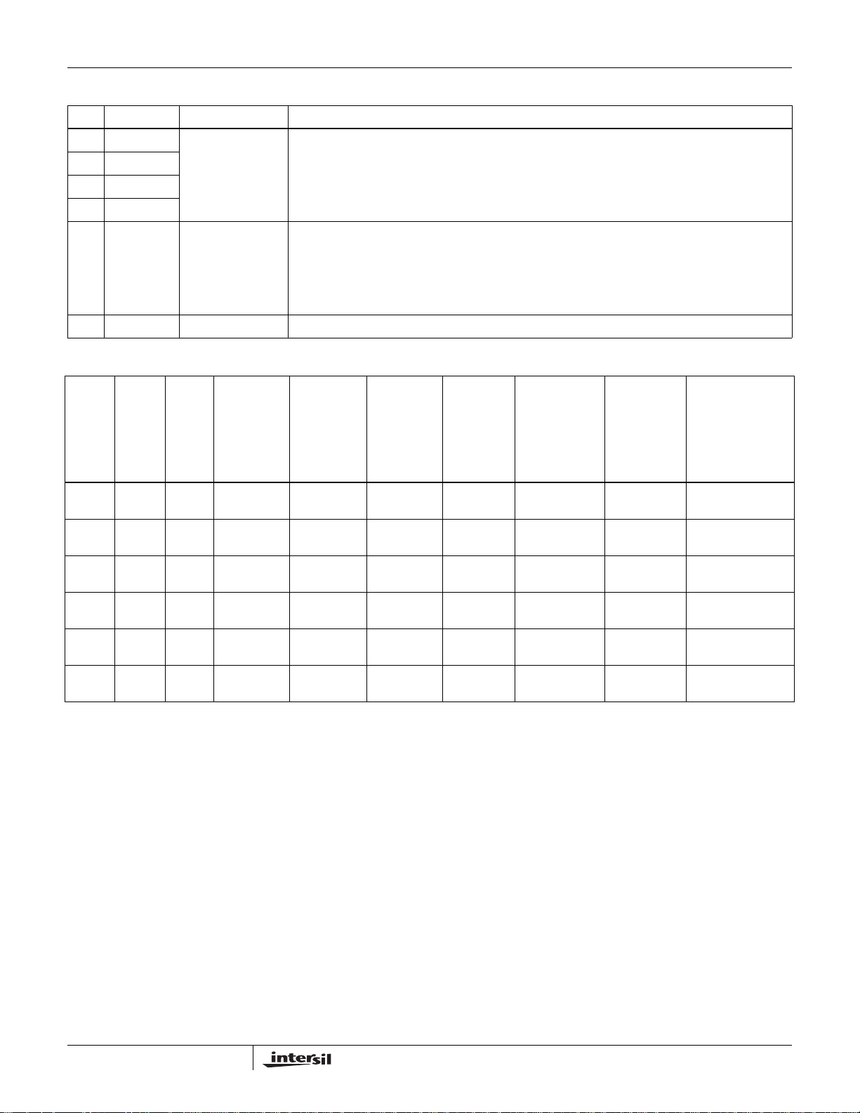
ISL612X Variant Feature Matrix
NUMBER OF
CHANNELS
THAT
TURN-OFF
WHEN 1
UVLO
FAULTS
PRESET OR
ADJUSTABLE
SEQUENCE
Off
Off
Off
NUMBER OF
UVLO AND
PAIRS OF I/O FEATURES
4 Monitors with
1 I/O
4 Monitors with
1 I/O
4 Monitors with
1 I/O
1 I/O
1 I/O
with 2 I/O
Auto restart
Auto restart
Auto restart
Gates independent
on as UVLO Valid
Auto restart
Dual Redundant
Operation
GATE DRIVE
OR OPEN
PAR T
NAME EN/EN#
ISL6123 EN TTL Gate Drive 4 UVLO
ISL6124 EN# CMOS Gate Drive 4UVLO
ISL6125 EN# CMO Open Drain 4 UVLO
ISL6126 EN# CMOS Gate Drive 1 UVLO
ISL6127 EN# CMOS Gate Drive 4 UVLO
ISL6128 EN# CMOS Gate Drive 4 UVLO
CMOS/
TTL
DRAIN
OUTPUTS
REQUIRED
CONDITIONS
FOR INITIAL
START-UP
1 EN
1 EN
1 EN
1 EN
1 EN
2 EN
NUMBER OF
UVLO
INPUTS
MONITORED
BY EACH
RESET#
4 UVLO 4 Gates Adjustable On &
4 UVLO 4 Gates Adjustable On &
4 UVLO 4 Open Drain Adjustable On &
4 UVLO 1 Gate Adjustable Off 4 Monitors with
4 UVLO 4 Gates Preset 4 Monitors with
2 UVLO 2 Gates Preset 2 Monitors
3
FN9005.4
June 10, 2005
Page 4
ISL6123, ISL6124, ISL6125, ISL6126, ISL6127, ISL6128
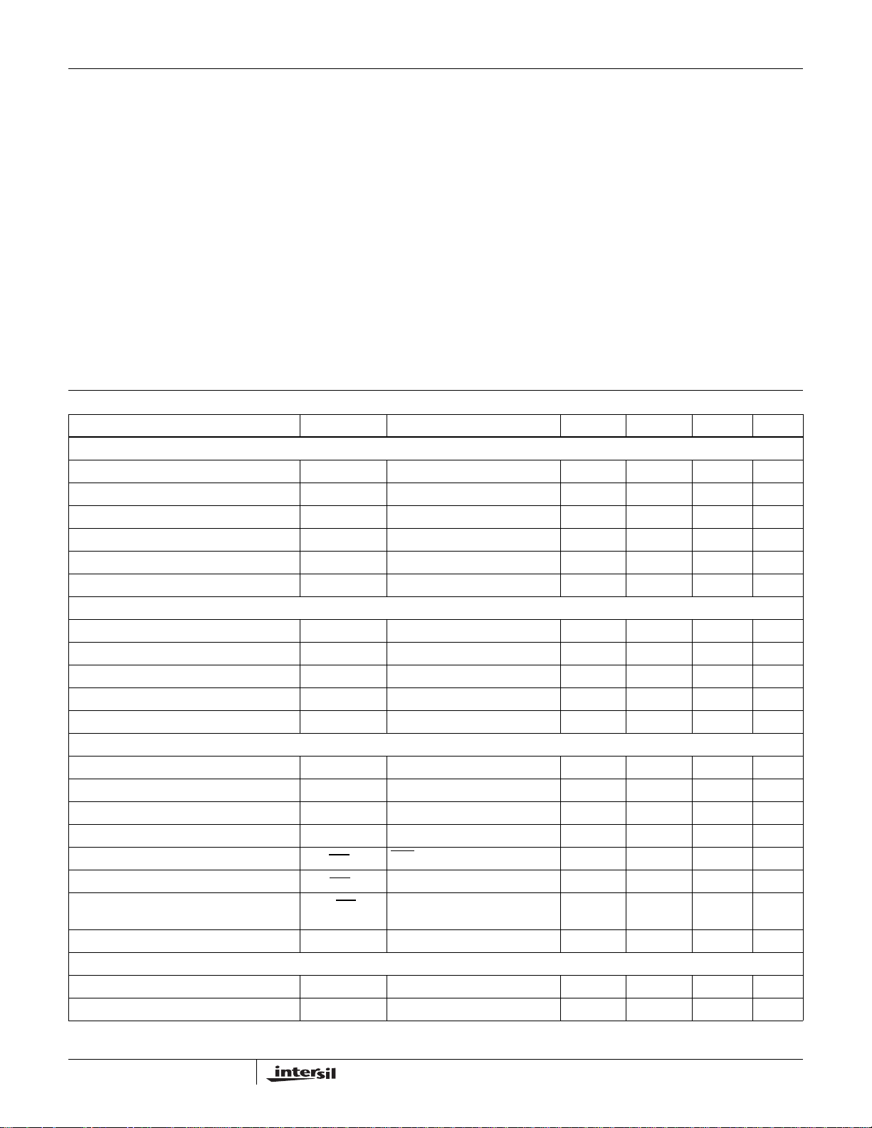
Absolute Maximum Ratings Thermal Information
VDD . . . . . . . . . . . . . . . . . . . . . . . . . . . . . . . . . . . . . . . . . . . . . +6.0V
GATE . . . . . . . . . . . . . . . . . . . . . . . . . . . . . . . . . . . -0.3V to V
ISL6125 LOGIC OUT. . . . . . . . . . . . . . . . . . . . . -0.3V to V
UVLO, ENABLE, ENABLE#, SYSRST# . . . . . . -0.3V to V
RESET#, DLY_ON, DLYOFF. . . . . . . . . . . . . . . -0.3V to V
ESD Classification . . . . . . . . . . . . . . . . . . . . . . . . . . . . 2.5kV (HBM)
DD
DD
DD
+6V
DD
+0.3V
+0.3V
+0.3V
Operating Conditions
VDD Supply Voltage Range . . . . . . . . . . . . . . . . . . . . +1.5V to +5.5V
Temperature Range (T
CAUTION: Stresses above those listed in “Absolute Maximum Ratings” may cause permanent damage to the device. This is a stress only rating and operation of the
device at these or any other conditions above those indicated in the operational sections of this specification is not implied.
NOTES:
is measured with the component mounted on a high effective thermal conductivity test board in free air. See Tech Brief TB379 for details.
1. θ
JA
2. For θ
, the “case temp” location is the center of the exposed metal pad on the package underside.
JC
3. All voltages are relative to GND, unless otherwise specified.
) . . . . . . . . . . . . . . . . . . . . . . . -40°C to 85°C
A
Thermal Resistance (Typical, Notes 1, 2) θ
(°C/W) θJC (°C/W)
JA
4 x 4 QFN Package . . . . . . . . . . . . . . . 48 9
Maximum Junction Temperature . . . . . . . . . . . . . . . . . . . . . . . . 150°C
Maximum Storage Temperature Range . . . . . . . . . . . -65°C to 150°C
Maximum Lead Temperature (Soldering 10s) . . . . . . . . . . . . . 300°C
(QFN - Leads Only)
Electrical Specifications V
= 1.5V to +5V, TA = T
DD
= -40°C - 85°C, Unless Otherwise Specified.
J
PARAMETER SYMBOL TEST CONDITIONS MIN TYP MAX UNIT
UVLO
Undervoltage Lockout Threshold V
Undervoltage Lockout Threshold Temp Co TC
Undervoltage Lockout Hysteresis V
UVLOvth
UVLOvthTJ
UVLOhys
Undervoltage Lockout Threshold Range RUVLOvth Max V
TJ = +25°C 619 633 647 mV
= -40°C to 85°C - 40 - nV/°C
-10-mV
UVLOvth
- Min V
UVLOvth
-7-mV
Undervoltage Lockout Delay TUVLOdel ENABLE satisfied - 10 - ms
Transient Filter Duration TFIL V
, UVLO, ENABLE glitch filter - 30 - µs
DD
DELAY ON/OFF
Delay Charging Current DLY_ichg V
= 0V 0.92 1 1.08 µA
DLY
Delay Charging Current Range DLY_ichg_r DLY_ichg(max) - DLY_ichg(min) - 0.08 - µA
Delay Charging Current Temp. Coeff. TC_DLY_ichg - 0.2 - nA/°C
Delay Threshold Voltage DLY_Vth 1.238 1.266 1.294 V
Delay Threshold Voltage Temp. Coeff. TC_DLY_Vth - 0.2 - mV/°C
ENABLE/ENABLE#, RESET# & SYSRST# I/O
ENABLE Threshold V
ENABLE# Threshold V
ENABLE/ENABLE# Hysteresis V
ENh -VENl
ENh
ENh
Measured at V
= 1.5V - 0.2 - V
DD
-1.2-V
-0.5 VDD-V
ENABLE/ENABLE# Lockout Delay TdelEN_LO UVLO satisfied - 10 - ms
RESET# Pull-Down Current I
RESET# Delay after GATE High T
RESET# Output Low V
SYSRST# Low to GATE Turn-off T
delSYS_G
RSTpd
RSTdel
RSTl
RST = 0.1V - 13 - mA
GATE = VDD+5V - 160 - ms
Measured at V
pullup resistors
= 5V with 5K
DD
- - 0.001 V
GATE = 80% of VDD+5V - 40 - ns
GATE
GATE Turn-On Current I
GATE Turn-Off Current I
GATEon
GATEoff_l
GATE = 0V 0.8 1.1 1.4 µA
GATE = VDD, Disabled -1.4 -1.05 -0.8 µA
4
FN9005.4
June 10, 2005
Page 5

ISL6123, ISL6124, ISL6125, ISL6126, ISL6127, ISL6128
Electrical Specifications V
PARAMETER SYMBOL TEST CONDITIONS MIN TYP MAX UNIT
GATE Current Range I
GATE Turn-On/Off Current Temp. Coeff. TC_I
GATE Pull-Down High Current I
GATE High Voltage V
GATE Low Voltage V
BIAS
IC Supply Current I
IC Supply Current I
IC Supply Current I
ISL6123 Stand By IC Supply Current I
V
Power On Reset VDD_POR - - 1 V
DD
ISL6123, 24, 25, 26, 27, 28 Descriptions
and Operation
The ISL612X sequencer family consists of several four
channel voltage sequencing controllers in various
functional and personality configurations. All are designed
for use in multiple-voltage systems requiring power
sequencing of various supply voltages. Individual voltage
rails are gated on and off by external N-Channel MOSFETs,
the gates of which are driven by an internal charge pump to
V
+5.3V (VQP) in a user programmed sequence.
DD
With the four-channel ISL6123 the ENABLE must be
asserted high and all four voltages to be sequenced must
be above their respective user programmed Under Voltage
Lock Out (UVLO) levels before programmed output turn on
sequencing can begin. Sequencing and delay
determination is accomplished by the choice of external
cap values on the DLY_ON and DLY_OFF pins. Once all 4
UVLO inputs and ENABLE are satisfied for 10ms, the four
DLY_ON caps are simultaneously charged with 1µA current
sources to the DLY_Vth level of 1.27V. As each DLY_ON
pin reaches the DLY_Vth level its associated GATE will
then turn-on with a 1µA source current to the VQP voltage
of V
+5.3V. Thus all four GATEs will sequentially turn on.
DD
Once at DLY_Vth the DLY_ON pins will discharge to be
ready when next needed. After the entire turn on sequence
has been completed and all GATEs have reached the
charge pumped voltage (VQP), a 160ms delay is started to
ensure stability after which the RESET# output will be
released to go high. Subsequent to turn-on, if any input
falls below its UVLO point for longer than the glitch filter
period (~30µs) this is considered a fault. RESET# and
SYSRST# are pulled low and all GATEs are simultaneously
also pulled low. In this mode the GATEs are pulled low with
88mA. Normal shutdown mode is entered when no UVLO
is violated and the ENABLE is deasserted. When ENABLE
is deasserted, RESET# is asserted and pulled low. Next, all
four shutdown ramp caps on the DLY_OFF pins are
= 1.5V to +5V, TA = T
DD
GATE_range
GATE
GATEoff_h
GATEh
GATE_
VDD_5V
VDD_3.3V
VDD_1.5V
VDD_sb
= -40°C - 85°C, Unless Otherwise Specified. (Continued)
J
Within IC I
GATE = VDD, UVLO = 0V - 88 - mA
Gate High Voltage VDD+5V VDD+5.3V - V
Gate Low Voltage, VDD = 1V - 0 0.1 V
V
= 5V - 0.20 0.5 mA
DD
V
= 3.3V - 0.14 - mA
DD
V
= 1.5V - 0.10 - mA
DD
V
= 5V, ENABLE = 0V - - 1 µA
DD
max-min - - 0.35 µA
GATE
-0.2-nA/°C
charged with a 1µA source and when any ramp-cap
reaches DLY_Vth, a latch is set and a current is sunk on
the respective GATE pin to turn off its external MOSFET.
When the GATE voltage is approximately 0.6V, the GATE is
pulled down the rest of the way at a higher current level.
Each individual external FET is thus turned off removing
the voltages from the load in the programmed sequence.
The ISL6123 and ISL6124 have the same functionality
except for the ENABLE active polarity with the ISL6124
having an ENABLE# input. Additionally the ISL6123 also
has an ultra low power sleep state when ENABLE is low.
The ISL6125 has the same personality as the ISL6124 but
instead of charged pump driven GATE outputs it has open
drain LOGIC outputs that can be pulled up to a maximum of
V
.
DD
The ISL6126 is unique in that it’s sequence on is not time
determined but voltage determined. It’s personality is that each
of the four channels operates independently so that once the IC
is biased and any one of the UVLO inputs is greater than the
0.63V internal reference, and ENABLE# input is also satisfied
the GATE for the associated UVLO input will turn-on. In turn the
other UVLO inputs need to be satisfied for the associated
GATEs to turn-on. 150ms after all GATEs are fully on (GATE
voltage = VQP) the RESET# is released to go high. The UVLO
inputs can be driven by either a previously turned on output rail
offering a voltage determined sequence or by logic signal
inputs. Any subsequent UVLO level < its programmed level will
pull the RESET# output low (if previously released), but will not
latch-off the other outputs. Predetermined turn-off is
accomplished by signaling ENABLE# high, this will cause
RESET# to latch low and all four GATE outputs to follow the
programmed turn off sequence similar to a ISL6124.
The ISL6127 is a four channel sequencer pre-programmed for
A-B-C-D turn-on and D-C-B-A turn-off. After all four UVLO and
ENABLE# inputs are satisfied for ~10ms, the sequencing starts
and the next GATE in the sequence starts to ramp up once the
5
FN9005.4
June 10, 2005
Page 6
ISL6123, ISL6124, ISL6125, ISL6126, ISL6127, ISL6128
previous GATE has reached ~VQP-1V. 160ms after the last
GATE is at VQP the RESET# output will be deasserted. Once
any UVLO is unsatisfied, RESET# is pulled low, SYSRST# is
pulled low and all GATEs are simultaneously turned off. When
ENABLE# is signaled high the D GATE will start to pull low and
once below 0.6V the next GATE will then start to pull low and so
on until all GATEs are at 0V. Unloaded, this turn off sequence
will complete in <1ms. This variant offers a lower cost and size
implementation as the external delay caps are not used. Since
the delay caps are not used this IC can not delay the start of
subsequent GATEs thus necessary stabilization or system
house keeping need to be considered.
The ISL6128 is a four channel device that groups the four
channels into two groups of two channels each, as A, B and
C, D. Each group having its own ENABLE# and RESET# I/IO
pins. This requires all four UVLO and both ENABLE#s to be
satisfied for sequencing to start. The A, B group will first turn on
10ms after the second ENABLE# is pulled low with A then B
turning on followed by C then D. Once the preceding GATE =
VQP the next DLY_ON pin starts to charge its capacitor thus
turning on all four GATEs. Approximately 160ms after D GATE
= VQP the RESET# output is released to go high. Once any
UVLO is unsatisfied, only the related group’s RESET# and two
GATEs are pulled low. The related EN input has to be cycled for
the faulted group to be turned-on again. Normal shutdown is
invoked by either signaling both ENABLE# inputs high which
will cause all the two related GATEs to shutdown in reverse
order from turn-on. DLY_X caps adjust the delay between
GATES during turn on and off but not the order.
During bias up the RESET# output is guaranteed to be in
the correct state with V
lower than 1V.
DD
The SYSRST# pin is a true I/O connection having both
functions. As an input, if it is pulled low all GATEs will
unconditionally shut off and RESET# pulls low, see Figure
6. This input can be used as a no wait enabling input, if all
inputs (ENABLE & UVLO) are satisfied it does not wait
through the ~10ms enable delay to initiate DLY_ON cap
charging. It is also useful when multiple sequencers are
implemented in a design needing simultaneous shutdown
(kill switch) across all sequencers. As an output, after the
on sequence is completed it will pull low after any UVLO is
unsatisfied longer than T
and pull all other SYSRST#
FIL
inputs low on common connection thus unconditionally
shutting down all outputs across multiple sequencers.
If no capacitors are connected between DLY_ON or
DLY_OFF pins and ground then all such related GATEs
start to turn on immediately after the 10ms (T
UVLOdel
)
ENABLE stabilization time out has expired and the GATEs
start to immediately turn off when ENABLE is asserted.
If some of the rails are to be sequenced together, in order to
eliminate the effect of capacitor variance on the timing and to
reduce cost, a common capacitor can be connected to two
or more DLY_ON or DLY_OFF pins. In this case multiply the
capacitor value by the number of common DLY_X pins to
retain the desired timing.
Table 1 illustrates the nominal time delay from the start of
charging to the 1.27V reference for various capacitor
values on the DLY_X pins. This table does not include the
10ms of enable lock out delay during a start up sequence
but represents the time from the end of the enable lock out
delay to the start of GATE transition. There is no enable
lock out delay for a sequence off, so this table illustrates
the delay to GATE transition from a disable signal.
TABL E 1 .
NOMINAL DELAY TO SEQUENCING THRESHOLD
DLY PIN CAPACITANCE TIME (s)
Open 0.00006
100pF 0.00013
1000pF 0.0013
0.01µF 0.013
0.1µF0.13
1µF1.3
10µF13
NOTE: Nom. T
DEL_SEQ
= Cap (µF) * 1.3MΩ.
Figure 2 illustrates the turn-on and Figure 3 the nominal turnoff
timing diagram of the ISL6123 and ISL6124 product.
The ISL6125 is similar except the open drains instead of GATE
pins are pulled up to V
DD
.
Note the delay and flexible sequencing possibilities.
Except ISL6128 after a fault, restart of the turn on
sequence is automatic once all requirements are met. This
allows for no interaction between the sequencer and a
controller IC if desired. The ENABLE & RESET# I/O do
allow for a higher level of feedback and control if desired.
The ISL6128 requires that the related ENABLE# be cycled
for restart of its associated group GATEs.
6
FN9005.4
June 10, 2005
Page 7

ISL6123, ISL6124, ISL6125, ISL6126, ISL6127, ISL6128
l
V
UVLO_A
UVLO_B
UVLO_C
UVLO_D
ENABLE# (ISL6124)
ENABLE (ISL6123)
DLYON_B
UVLOVth
V
UVLOVth
V
UVLOVth
V
UVLOVth
T
UVLOdel
V
EN
DLY_Vth
DLY_Vth
<TFIL
DLYON_D
DLY_Vth
DLYON_A
DLY_Vth
DLYON_C
GATE_B
GATE_D
V
GATE_C
QPUMP
GATE_A
RESET#
FIGURE 2. ISL6123/ISL6124 TURN-ON AND GLITCH RESPONSE TIMING DIAGRAM
UVLO_X>VUVLOVth
ENABLE(ISL6123)
ENABLE# (ISL6124)
DLYOFF_A
DLYOFF_B
DLYOFF_C
DLYOFF_D
V
EN
DLY_Vth
DLY_Vth
DLY_Vth
DLY_Vth
-1V
T
RSTdel
V
QPUMP
V
QPUMP
V
QPUMP
V
QPUMP
GATE_C
GATE_D
GATE_A
GATE_B
RESET#
FIGURE 3. ISL6123/ISL6124 TURN-OFF TIMING DIAGRAM
7
FN9005.4
June 10, 2005
Page 8
ISL6123, ISL6124, ISL6125, ISL6126, ISL6127, ISL6128
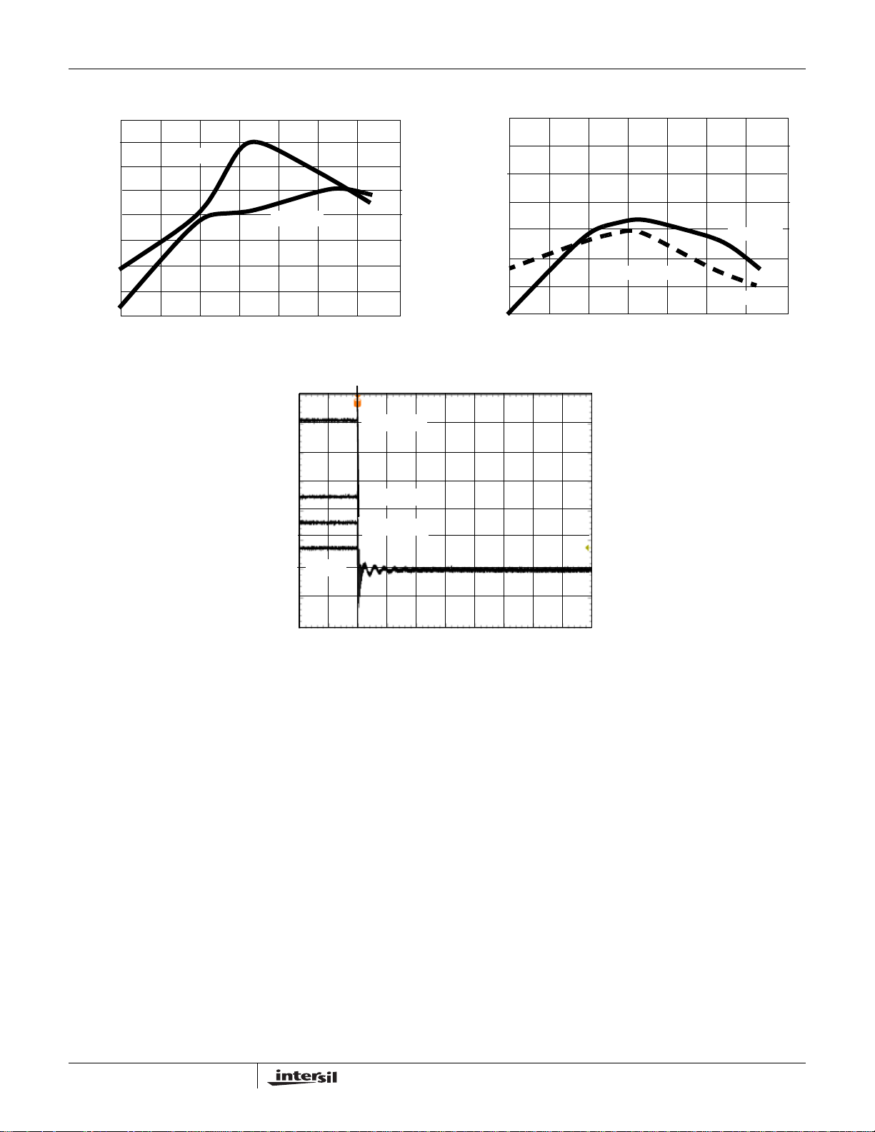
Typical Performance Curves
634
633
632
631
630
629
UV THRESHOLD (mV)
628
627
626
-40 0 20 60-20 40 80 100
FIGURE 4. UVLO THRESHOLD VOLTAGE FIGURE 5. DLY CHARGE CURRENT
V
= 5V
DD
TEMPERATURE (°C)
V
DD
= 1.5V
GATE
1.04
1.03
1.02
1.01
1.00
0.99
0.98
DLY CURRENT SOURCE (µA)
0.97
-40 0 20 60-20 40 80 100
DLY_OFF/ON
TEMPERATURE (°C)
VDD = 1.5V
V
= +5V
DD
5VOUT
3.3VOUT
SYSRST#
2V/DIV
FIGURE 6. SYSRST# LOW TO OUTPUT LATCH OFF
Using the ISL612XSEQEVAL1 Platform
The ISL612XSEQEVAL1 platform is the primary evaluation
board for this family. The board has 2 complete, separate
and electrically identical circuits, see Figure 15 for schematic
and Figure 16 for a photo.
In the top right hand corner of the board is a SMD layout with
a ISL6123 illustrating the full functionality and small
implementation size for an application having the highest
component count.
The majority of the board is given over to a socket and
discrete through-hole components circuit for ease of
evaluation flexibility through IC variant swapping and
modification of UVLO levels and sequencing order by
passive component substitution.
The board is shipped with the ISL6123 installed in both
locations and with two each of the other released variant
types loose packed. As this sequencer family has a common
function pinout there are no major modifications to the board
1µs/DIV
necessary to evaluate the other ICs. The ISL6125 due to its
having open drain outputs can be evaluated on the
ISL612XSEQEVAL1 with a minor modification or on the
ISL613XSUPEREVAL2 evaluation platform. To modify for
ISL6125 evaluation, pull-up resistors must be added from
the GATE outputs to a pull-up voltage of 1.5V to prevent FET
turn-on or remove FETs to eliminate this voltage restriction.
To the left, right and above the socket are four test point
strips (TP1-TP4). These give access to the labeled IC I/O
pins during evaluation. Remember that significant current or
capacitive loading of particular I/O pins will affect
functionality and performance.
Attention to orientation and placement of variant ICs in the
socket must be paid to prevent IC damage or faulty
evaluation.
The default configuration of the ISL612XSEQEVAL1
circuitries was built around the following design
assumptions:
8
FN9005.4
June 10, 2005
Page 9

ISL6123, ISL6124, ISL6125, ISL6126, ISL6127, ISL6128
1. Using the ISL6123IR or ISL6124IR
2. The four supplies being sequenced are 5V (IN_A), 3.3V
(IN_B), 2.5V (IN_C) and 1.5V (IN_D), the UVLO levels
are ~ 80% of nominal voltages. Resistors chosen such
that the total resistance of each divider is ~ 10K using
standard value resistors to approximate 80% of
nominal = 0.63V on UVLO input.
3. The desired order turn-on sequence is first both 5V and
3.3V supplies together and then the 2.5V supply about
75ms later and lastly the 1.5V supply about 45ms later.
4. The desired turn-off sequence is first both 1.5V and 3.3V
supplies at the same time then the 2.5V supply about
50ms later and lastly the 5V supply about 72ms after that.
All scope shots taken from ISL612xSEQEVAL1 board.
Figures 7 and 8 illustrate the desired turn-on and turn-off
sequences respectively. The sequencing order and delay
between voltages sequencing is set by external capacitance
values so other than illustrated can be accomplished.
Figures 9 and 10 illustrate the timing relationships between
the EN input, RESET#, DLY and GATE outputs and the
VOUT voltage for a single channel being turned on and off
respectively. RESET# is not shown in Figure 9 as it asserts
160ms after the last GATE goes high.
All IC family variants share similar function for DLY_X
capacitor charging, GATE and RESET# operation. Figures
11 through 14 illustrate the principal feature and functional
differences for each of the ISL6125, ISL6126, ISL6127 and
ISL6128 variants, each is described below.
Figure 11 features the 6125 open drain outputs being
sequenced on and off along with RESET# relatiionship
which is similar to all other family variants.
Figure 12 illustrates the independent input feature of the
ISL6126 which allows once the EN# is low for each UVLO to
be individually satisfied and for its associated GATE to turnon. Only when the last variable VIN is satisfied as shown
does the RESET# release to signal all input voltages are
valid.
Figure 13 shows the ISL6127 pre programmed ABCD on
DCBA off order of sequencing with minimal non adjustable
delay between each.
Figure 14 demonstrates the independence of the redundant
two rail sequencer. It shows that either one of the two groups
can be turned off and the ABCD order of restart with
capacitor programmable delay once both EN inputs are
pulled low.
Typical Performance Waveforms
5VOUT
ENABLE#
1V/DIV 40ms/DIV
FIGURE 7. ISL6124 SEQUENCED TURN-ON
3.3VOUT
2.5VOUT
1.5VOUT
RESET#
5VOUT
3.3VOUTPUT
2.5VOUT
1.5VOUT
ENABLE#
1V/DIV 20ms/DIV
FIGURE 8. ISL6124 SEQUENCED TURN-OFF
9
FN9005.4
June 10, 2005
Page 10

ISL6123, ISL6124, ISL6125, ISL6126, ISL6127, ISL6128
Typical Performance Waveforms (Continued)
T
delENLO
GATE 2V/DIV
GATE 2V/DIV
3.3VO 1V/DIV
DLY_Vth
DLY_ON 1V/DIV
EN 2V/DIV
10ms/DIV
3.3VO 1V/DIV
RESET# 2V/DIV
EN 2V/DIV
DLY_Vth
DLY_OFF 1V/DIV
4ms/DIV
FIGURE 9. ISL6123 SINGLE CHANNEL TURN-ON FIGURE 10. ISL6123 SINGLE CHANNEL TURN-OFF
EN#
RESET#
VIN_VAR
STATIC EN/ALL OTHER VOUT
VOUT_VAR
LOGIC A-D STATUS
OUTPUTS
T
RSTdel
100ms/DIV
FIGURE 11. ISL6125 LOGIC OUTPUTS SEQUENCED ON AND
OFF AND RESET# RELATIONSHIP
A_VOUT
B_VOUT
C_VOUT
D_VOUT
FIGURE 13. ISL6127 PREPROGRAMMED ABCD TURN-ON AND
DCBA TURN-OFF
RESET#
100ms/DIV
FIGURE 12. ISL6126 UVLO INPUT/OUTPUT INDEPENDANCE
AND RESET# RELATIONSHIP
EN#_1 5V/DIV
EN#_2 5V/DIV
A_VOUT
B_VOUT
C_VOUT
D_VOUT
FIGURE 14. ISL6128 GROUP INDEPENDANT TURN-OFF & DELAY
ADJUSTABLE PREPROGRAMMED TURN-ON
10
FN9005.4
June 10, 2005
Page 11

ISL6123, ISL6124, ISL6125, ISL6126, ISL6127, ISL6128
+2.5V1.5V+3.3V
EN1
EN2
SYSRST#
1
1
R5
R3
R1
7.681K 4.99K 5.98K 5.45K
R2 R5
2.26K
1
R4
4.99K
3.01K
R6
1.47K
+5V
23
ENABLE1
ENABLE2
UVLO_B
UVLO_D
UVLO_A
ISL6123IR
SYSRST#
NC
V
DD
DLY_ON_B
DLY_ON_D
DLY_ON_C
DLY_ON_A
U1
DLY_OFF_C
DLY_OFF_D
DLY_OFF_BUVLO_C
DLY_OFF_A
GATE_A
GATE_B
GATE_C
GATE_D
RESET#2
RESET#1
GND
10
1
11
R7
12
14
17
20
22
19
C1
1µF
C2
8
0.01µF
15
C3
16
0.068µF
21
C4
3
0.047µF
4
C5
13
0.01µF
18
2
5
6
7
20
9
24
1
R9
750
C6
0.1µF
C7
0.01µF
C8
0.01µF
C9
0.1µF
R10
750
6
5
SI4922DY
4
Q1
3
RL5 10 RL3 5 RL2 5
7
SI4922DY
8
2
Q1
1
5
4
3
6
SI4922DY
Q2
2
RL1
SI4922DY
7
8
Q2
1
2
FIGURE 15. EVAL BOARD SCHEMATIC
11
FIGURE 16. EVAL BOARD PHOTOGRAPH
FN9005.4
June 10, 2005
Page 12

ISL6123, ISL6124, ISL6125, ISL6126, ISL6127, ISL6128
TABLE 2. ISL612XSEQEVAL1 BOARD COMPONENT LISTING
COMPONENT
DESIGNATOR COMPONENT FUNCTION COMPONENT DESCRIPTION
DUT1 ISL6124, 4 Supply Sequencer Intersil, ISL6124IR 4 Supply Sequencer
Q1, Q2 Voltage Rail Switches SI4922DY or equiv, Dual 8A, 30V, 0.018Ω, N-Channel MOSFET
R7 5V to UVLO_A Resistor for Divider String 8.45kΩ 1%, 0402
R8 UVLO_A to GND Resistor for Divider String 1.47kΩ 1%, 0402
R1 3.3V to UVLO_B Resistor for Divider String 7.68kΩ 1%, 0402
R2 UVLO_B to GND Resistor for Divider String 2.26kΩ 1%, 0402
R5 2.5V to UVLO_C Resistor for Divider String 6.98kΩ 1%, 0402
R6 UVLO_C to GND Resistor for Divider String 3.01kΩ 1%, 0402
R3 1.5V to UVLO_D Resistor for Divider String 4.99kΩ 1%, 0402
R4 UVLO_D to GND Resistor for Divider String 4.99kΩ 1%, 0402
R9 RESET#1 LED Current Limiting Resistor 750Ω 10%, 0805
R10 RESET#2 LED Current Limiting Resistor 750Ω 10%, 0805
C7 5V turn-on Delay Cap. (13ms) 0.01µF 10%, 6.3V, 0402
C9 5V turn-off Delay Cap. (130ms) 0.1µF 10%, 6.3V, 0402
C2 3.3V turn-on Delay Cap. (13ms) 0.01µF 10%, 6.3V, 0402
C5 3.3V turn-off Delay Cap. (3ms) 0.01µF 10%, 6.3V, 0402
C3 2.5V turn-on Delay Cap. (88ms) 0.068µF 10%, 6.3V, 0402
C4 2.5V turn-off Delay Cap. (61ms) 0.047µF 10%, 6.3V, 0402
C6 1.5V turn-on Delay Cap. (130ms) 0.1µF 10%, 6.3V, 0402
C8 1.5V turn-off Delay Cap. (13ms) 0.01µF 10%, 6.3V, 0402
C1 Decoupling Capacitor 0.1µF, 0805
D1 RESET#1 Indicating LED 0805, SMD LEDs Red
D2 RESET#2 Indicating LED 0805, SMD LEDs Red
TP1 - TP24 Test Points Number Corresponds to DUT Pin Number
RL5 5V Load Resistor 10Ω 20%, 3W Carbon
RL3 3.3V Load Resistor 5Ω 20%, 3W Carbon
RL2 2.5V Load Resistor 5Ω 20%, 3W Carbon
RL1 1.5V Load Resistor 2Ω 20%, 3W Carbon
12
FN9005.4
June 10, 2005
Page 13

ISL6123, ISL6124, ISL6125, ISL6126, ISL6127, ISL6128
Application Implementations
Multiple Sequencer Implementations
In order to control the sequencing of more than 4 voltages,
several of the ISL6123, ISL6124, ISL6125 or ISL6127
devices can be variously configured together to accomplish
this. There may be concerns of a particular implementation
that would make a particular configuration preferable over
another. The fundamental questions to answer to determine
which configuration is best suited for your applications are;
1. What level of voltage assurance is needed prior to
sequencing on and can the voltage supplies be grouped
into high and low criticality?
2. Is there a critical maximum time window all supplies must
be present at load or is there a first and a second group
preference possibly with some work done in between the
two groups of voltages being present?
Three configurations are described and illustrated here.
In applications where the integrity of critical voltages must be
assured prior to sequencing, additional monitoring of the
critical supplies is needed. If the compliance of the voltage is
critical for either under voltage and or over voltage the
ISL613X family of supervisors can be employed to provide
this additional assurance across multiple sequencers, see
document FN9115 for supervisor data sheet. Figure 17 is a
block diagram of this voltage compliant, high assurance, low
risk configuration showing the ISL613X supervisor and a mix
of FET switched outputs and logic output sequencers
(ISL6124 and ISL6125 ICs).
If the mere presence of some voltage potential is adequate
prior to sequencing on then a small number of standard logic
AND gates can be used to accomplish this. The block
diagram in Figure 18 illustrates this voltage presence
configuration.
OE
LOW = RESET
UVLO
SYSRST#
ISL6124
en
RESET#’
POWER
SUPPLY
# N
UVLO
RESET#
ENABLE#
ENABLE#
SYSRST#
ISL6125
# N+1
RESET#
UVLO
G
A
T
E
L
O
G
I
C
ISL613Xs
MONITORING
ON ALL RAILS
PGOOD
en
RESET#
POWER
SUPPLY
FIGURE 17. ISL612X & ISL613X VOLTAGE COMPLIANT
VMON
SYSRST#
ISL6124
# N
UVLO
RESET#
ENABLE#
ENABLE#
SYSRST#
ISL6125
# N+1
RESET#
UVLO
SEQUENCING BLOCK DIAGRAM
OE
LOW = RESET
G
A
T
E
L
O
G
I
C
FIGURE 18. MULTIPLE ISL612X USING LOGIC GATES FOR
VOLTAGE PRESENCE DETECT
In either case the sequencing is straight forward across
multiple sequencers as all DLY_ON capacitors will
simultaneously start charging ~10ms after the common
ENABLE input signal is delivered. This allows the choice of
capacitors to be related to each other no different than using
a single sequencer. When the common enabling signal is
deasserted these configurations will then execute the turnoff sequence across all sequencers as programmed by the
DLY_OFF capacitor values.
In both cases with all the SYSRST# pins bussed together
once the on sequence is complete simultaneous shutdown
upon any UVLO input failure is assured as SYSRST# output
will momentarily pull low turning off all GATE and LOGIC
outputs.
There may be applications that require or allow groups of
supplies being brought up in sequence and supplies within
each group to be sequenced. Figure 19 illustrates such a
configuration that allows the first group of supplies to turn-on
before the second group starts. This arrangement does not
necessarily preclude adding the assurance of all supplies
prior to turn-on sequencing as previously shown but it will
13
FN9005.4
June 10, 2005
Page 14

ISL6123, ISL6124, ISL6125, ISL6126, ISL6127, ISL6128
prevent the turn-on sequence from completing if there is one
unsatisfied UVLO input in a group. Using this configuration
involves waiting through the T
UVLOdel
and T
RSTdel
(total of
~160ms) for each sequencer IC in the chain for the final
RESET# to release. Once ENABLE on the first sequencer is
deasserted all the RESET# outputs will quickly pull low and
thus allow the sequenced turn-off of this configuration to
ripple through several banks as quickly as the user
programmed sequence as chosen by the DLY_OFF
capacitors allow. Once again with common bussed
SYSRTS# pins, simultaneous shut down of all GATEs and
LOGIC down upon an unsatisfied UVLO input is assured
once all FETs or LOGIC output are on.
OE
LOW= RESET
SYSRST#
ISL6124
ENABLE
# N
UVLO
ENABLE#
G
A
T
E
It is suggested that this circuit implementation be prototyped
and evaluated for the particular expected loads prior to
committing to manufacturing build.
FIGURE 20. OUTPUT VOLTAGE ON LOW TO HIGH TRACKING
RESET#
ENABLE#
SYSRST#
ISL6125
# N+1
POWER
SUPPLY
FIGURE 19. MULTIPLE ISL612X SERIAL CONFIGURATION
RESET#
UVLO
RESET#
RESET#
L
O
G
I
C
Voltage Tracking
In some applications the various voltages may have to track
each other as they ramp up & down whereas others may just
need sequencing. In these cases tracking can be
accomplished and has been demonstrated over a wide
range of load current (1A to 10A) and load capacitance
(10µF to 3300µF) with the ISL612X family. Figures 20 and
21 illustrate output voltage ramping tracking performance,
note that differences are less than 0.5V. With the relevant
GATE pins tied together in a star pattern, so that the
resistance between any two GATE pins is equivalent (1K to
10K) results in a sharing of the GATE ramping voltage and
with the same or similar enough FETs this behavior is
observed.
FIGURE 21. OUTPUT VOLTAGE HIGH TO LOW TRACKING
Negative Voltage Sequencing
They ISL612X family can use the charged pump GATE
output to drive FETs that would control and sequence
negative voltages down to a nominal -5V with minimal
additional external circuitry. Figure 22 shows turn-on of 5V
bipolar supplies together then the +2.5V and turn-off of both
positive supplies being turned off together after the -5V.
Figure 23 shows the minimal additional external circuitry to
accomplish this. The 5V zener diode is used to level shift the
GATE drive down 5V to prevent premature turn-on when
GATE = 0V. Once GATE drive voltage > Vz then FET Vgs >
5V ensuring full turn-on once GATE gets to VDD+5.3V. Turnon and turn-off ramp rate can be adjusted with FET gate
series resistor value. Sequencing of the -V rail is
accomplished as normal via the DLY_X capacitor value
although adjustments in prototyping should be factored in to
fine tune for actual circuit requirements.
14
FN9005.4
June 10, 2005
Page 15

ISL6123, ISL6124, ISL6125, ISL6126, ISL6127, ISL6128
Figures 24 and 25 illustrate a high accuracy -V detection
circuit using the ISL6131and a low cost low accuracy -V
detect circuit and respectively.
FIGURE 22. ±VOLTAGE SEQUENCING
-Vin
R1
ISL612X GATE
D1
Additional 2 components
necessary for -V control
and sequencing.
D1 necessary to prevent premature turn-on. R1 is used
to hold FET Vgs = 0V until D1 Vz is overcome. R1 value
can be changed to adjust -V ramp rates. Choose a R1
value between 4MΩ and 10MΩ initially and fine tune
resistor value for the particular need.
FIGURE 23. -VOLTAGE FET DRIVE CIRCUIT
+V
R1
VMON
R2
-V
R1 and R2 define -V UVLO level
R3 ensures supervisor (ISL6131 or ISL6536A) PGOOD pull-up
R4 and R5 provide Q1 gate bias between 0V and +V
to 0V (resistor values suitable for -V = -5V and +V = +3.3V)
+BIAS
ISL6131
OR
ISL6536A
-BIAS
PGOOD
R3
(1K)
(15K)
R4
R5
(10K)
R6
Q1 Si1300DL
OR EQUIV.
FIGURE 24. HGH ACCURACY -V LOCK OUT
-Vout
TO UVLO OF
ISL612X FOR
-V CONTROL AND
SEQUENCING
Application Considerations
Timing Error Sources
In any system there are variance contributors, for the ISL612X
family the timing errors are mainly contributed by three sources.
Capacitor Timing Mismatch Error
Obviously, the absolute capacitor value is an error source
thus lower percentage tolerance capacitors help to reduce
this error source. Figure 26 illustrates a difference of 0.57ms
between two DLY_X outputs ramping to DLY_X threshold
voltage, these 5% capacitors were from a common source.
In applications where two or more GATEs or LOGIC outputs
must have concurrent transitions, it is recommended that a
common DLY_X cap. be used to eliminate this timing error.
FIGURE 26. CAPACITOR TIMING MISMATCH
DLY_X Threshold Voltage and Charging Current
Mismatch
The two other error sources come from the IC itself and are
the differences in the DLY_X threshold voltage, (DLY_Vth)
when the GATE charging latch is set and the DLY_X
charging current, (DLY_ichg) across the four individual I/Os.
Both of these parameters are bounded by specification and
Figure 27 illustrates that with a common capacitor the typical
error contributed by these factors is insignificant as both
DLY_X traces overlay each other.
+V
R1
TO UVLO OF ISL612X FOR CONTROL
AND SEQUENCING OF -V
R2
-V
Chose R1 and R2 values to drive UVLO
high when -V is sufficiently present
FIGURE 25. LOW ACCURACY -V PRESENCE DETECTION
15
FIGURE 27. DLY_VTH AND DLY_ICHG TIMING MISMATCH
FN9005.4
June 10, 2005
Page 16

ISL6123, ISL6124, ISL6125, ISL6126, ISL6127, ISL6128
Quad Flat No-Lead Plastic Package (QFN)
Micro Lead Frame Plastic Package (MLFP)
L24.4x4
24 LEAD QUAD FLAT NO-LEAD PLASTIC PACKAGE
(COMPLIANT TO JEDEC MO-220VGGD-2 ISSUE C)
MILLIMETERS
SYMBOL
A 0.80 0.90 1.00 -
A1 - - 0.05 -
A2 - - 1.00 9
A3 0.20 REF 9
b 0.18 0.23 0.30 5, 8
D 4.00 BSC -
D1 3.75 BSC 9
D2 1.95 2.10 2.25 7, 8
E 4.00 BSC -
E1 3.75 BSC 9
E2 1.95 2.10 2.25 7, 8
e 0.50 BSC -
k0.25 - - -
L 0.30 0.40 0.50 8
L1 - - 0.15 10
N242
Nd 6 3
Ne 6 3
P- -0.609
θ --129
NOTES:
1. Dimensioning and tolerancing conform to ASME Y14.5-1994.
2. N is the number of terminals.
3. Nd and Ne refer to the number of terminals on each D and E.
4. All dimensions are in millimeters. Angles are in degrees.
5. Dimension b applies to the metallized terminal and is measured
between 0.15mm and 0.30mm from the terminal tip.
6. The configuration of the pin #1 identifier is optional, but must be
located within the zone indicated. The pin #1 identifier may be
either a mold or mark feature.
7. Dimensions D2 and E2 are for the exposed pads which provide
improved electrical and thermal performance.
8. Nominal dimensions are provided to assist with PCB Land Pattern
Design efforts, see Intersil Technical Brief TB389.
9. Features and dimensions A2, A3, D1, E1, P & θ are present when
Anvil singulation method is used and not present for saw
singulation.
10. Depending on the method of lead termination at the edge of the
package, a maximum 0.15mm pull back (L1) maybe present. L
minus L1 to be equal to or greater than 0.3mm.
NOTESMIN NOMINAL MAX
Rev. 2 10/02
All Intersil U.S. products are manufactured, assembled and tested utilizing ISO9000 quality systems.
Intersil Corporation’s quality certifications can be viewed at www.intersil.com/design/quality
Intersil products are sold by description only. Intersil Corporation reserves the right to make changes in circuit design, software and/or specifications at any time without
notice. Accordingly, the reader is cautioned to verify that data sheets are current before placing orders. Information furnished by Intersil is believed to be accurate and
reliable. However, no responsibility is assumed by Intersil or its subsidiaries for its use; nor for any infringements of patents or other rights of third parties which may result
from its use. No license is granted by implication or otherwise under any patent or patent rights of Intersil or its subsidiaries.
For information regarding Intersil Corporation and its products, see www.intersil.com
16
FN9005.4
June 10, 2005
 Loading...