

Page 1
®
www.BDTIC.com/Intersil
ISL6113, ISL6114
Data Sheet September 25, 2007
Dual Slot PCI-E Hot Plug Controllers
The ISL6113, ISL6114 both target the PCI-Express Add-in card
hot swap application. Together with a pair of N-Channel and
P-Channel MOSFETs, and two sense resistors per slot, either
provides compliant hot plug power control to any combination
of two PCI-Express X1, X4, X8 or X16 slots.
The ISL6113, ISL6114 feature a programmable current
regulated (CR) maximum level for a programmable period to
each voltage load so that both fault isolation protection and
imperviousness to electrical transients are provided.
For each +12V supply, the CR level is set by a resistor value
depending on the needs of the PCI-Express connector (X1, X4,
X8 or X16) to be powered. This resistor is a sub-ohm standard
value current sense resistor one for each slot and the voltage
across this resistor is compared to a 50mV reference providing
a nominal CR protection level adequately above the specific
slot maximum limits. The 3.3V supply uses a 15mΩ sense
resistor compared to a 50mV reference to provide 3.3A of
maximum regulated current to all connector sizes. The
3.3VAUX is internally monitored and controlled to provide a
nominal maximum of 1A of AUX output current.
FN6457.0
FN6457.0
Features
• Dual PCI-E Slot Hot Swap Power Control and Distribution
• Highest Accuracy External R
Current Monitoring
SENSE
On Main Supplies
• Programmable Current Regu lation Prot ection F unctio n for
X1, X4, X8, X16 Connectors
• Programmable Current Regu lation Durati on
• Programmable In-rush Protecti on Duri ng Turn-On
• Latch-off or Retry Modes After Failure
• Pb-free (RoHS Compliant)
Applications
• PCI-Express Servers
• Power Supply Distribution and Control
• Hot Swap/Electronic Breaker Circuits
• Network Hubs, Routers, Switches
• Hot Swap Bays, Cards and Modules
The CR period for each slot is set by a separate external
capacitor on the associated CFILTER pin. Once the CR period
has expired, the IC then quickly turns off its associated FETs
thus unloading the faulted card from the supply voltage rails. A
nominal 3.3V must always be present on the AUXI pin for
proper IC bias; this should be the 3.3VAUX supply if used, if not
the AUXI pin is tied directly to the 3VMAIN supply. Both ICs
employ a card presence detection input that disables the MAIN
and AUX enabling inputs if it is not pulled low. Output voltage
monitoring with both PCI-E Reset Not and Power Good Not
reporting along with OC Fault reporting are provided. Whereas
the ISL6113 has the same GATE drive and response
characteristics as the ISL6112, the ISL6114 has a lower turn-on
GA TE drive curr ent allo wing for the use of smaller
compensation capacitors and thus much faster response to
Way Overcurrent (WOC) conditions. Additionally, the ISL6114
does not turn-on with the CR feature invoked as do the
ISL6112, ISL6113 all owing for sho rter CR progra mmed
periods.The ISL6113, ISL6114 are footprint compatible for all
common pins, but not entirely function compatible with the
ISL61 12’ s QFN package as there ar e I/O dif ferences.
IF 3.3VAUX NOT
IMPLEMENTED
12VSENSEA
12VINA
VSTBYA
PRSNTB
PRSNTA
FORONA
FORONB
AUXENA
ONA
AUXENB
ONB
GPI_A0
GPI_BO
CFILTERA
CFILTERB
GND
VSTBYB
12VINB 3SENSEB
12VSENSEB
IF 3.3VAUX NOT
IMPLEMENTED
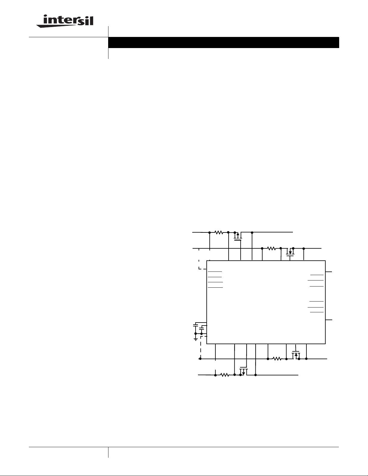
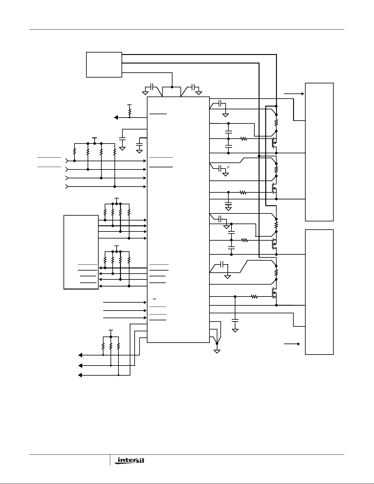
FIGURE 1. TYPICAL ISL6113, ISL6114 BLOCK DIAGRAM
APPLICATION IMPLEMENTATION
12VOUTA
12VGATEA
12VGATEB
12VOUTB
ISL6113, ISL6114
3VINA
3VINB
3VSENSEA
3VGATEA
3VGATEB
3VOUTA
3VOUTB
VAUXA
FAULTA
PWRGDA
PERSTA
GPO_A0
GPO_B0
PERSTB
PWRGDB
FAULTB
VAUXB
1
CAUTION: These devices are sensitive to electrostatic discharge; follow proper IC Handling Procedures.
1-888-INTERSIL or 1-888-468-3774
| Intersil (and design) is a registered trademark of Intersil Americas Inc.
All other trademarks mentioned are the property of their respective owners.
Copyright Intersil Americas Inc. 2007. All Rights Reserved
Page 2
ISL6113, ISL6114
www.BDTIC.com/Intersil
Ordering Information
PART
NUMBER
ISL6113IRZA ISL6113 IRZ -40 to +85 48 Ld 7x7 QFN L48.7x7
ISL6113IRZA-T* ISL6113 IRZ -40 to +85 48 Ld 7x7 QFN Tape and Reel L48.7x7
ISL6114IRZA ISL6114 IRZ -40 to +85 48 Ld 7x7 QFN L48.7x7
ISL6114IRZA-T* ISL6114 IRZ -40 to +85 48 Ld 7x7 QFN Tape and Reel L48.7x7
ISL6113EVAL1Z ISL6113 Evaluation Platform
ISL6114EVAL1Z ISL6114 Evaluation Platform
*Please refer to TB347 for details on reel specifications.
NOTE: These Intersil Pb-free plastic packaged products employ special Pb-free material sets; molding compounds/die attach materials and 100%
matte tin plate PLUS ANNEAL - e3 termination finish, which is RoHS compliant and compatible with both SnPb and Pb-free soldering operations.
Intersil Pb-free products are MSL classified at Pb-free peak reflow temperatures that meet or exceed the Pb-free requirements of IPC/JEDEC J
STD-020.
PART
MARKING
TEMP. RANGE
(°C)
PACKAGE
(Pb-free) PKG. DWG. #
Pinout
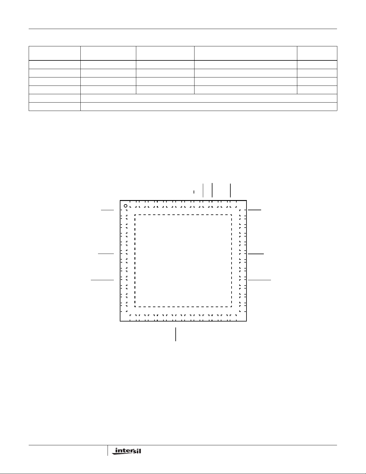
ISL6113, ISL6114
(48 LD QFN)
TOP VIEW
B
A
FAULT
CFILTERA
12VGATEA
GPI_A0
12VINA
PWRGDA
12VSENSEA
FORCE_ON
12VOUTA
VSTBYA
3VINA
NC
GPO_A0
GPO_B0
48 47 46 45 44 43 42 41 40 39 38 37
1
A
2
3
4
5
6
7
8
9
A
10
11
12
13 14 15 16 17 18 19 20 21 22 23 24
3VGATEA
3VSENSEA
AUXENA
GND
VAUXA
ONA
ONB
AUXENB
GND
(EXPOSED BOTTOM PAD)
GND
(Exposed bottom pad)
B
GND
3VOUTA
NC
PERST
L/R
NC
PRSNT
PRSNT
VAUXB
3VOUTB
GPI_B0
3VGATEB
PERSTA
36
35
34
33
32
31
30
29
28
27
26
25
3VSENSEB
FAULTB
CFILTERB
12VGATEB
GND
12VINB
B
PWRGD
NC
12VSENSEB
FORCE_ON
12VOUTB
VSTBYB
3VINB
B
2
FN6457.0
September 25, 2007
Page 3
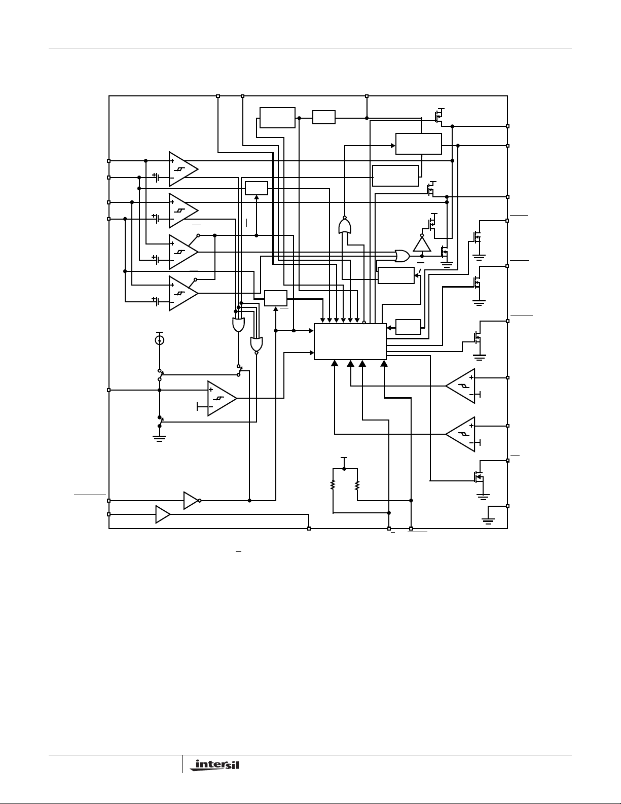
Functional Block Diagram (1 Channel)
www.BDTIC.com/Intersil
ISL6113, ISL6114
12VSENSE
12VIN
3VSENSE
3VIN
CFILTER
50mV
50mV
100mV*
100mV*
VSTBY
I
REF
1.25V
ON/OFF
ON
/OFF
ON AUXEN
12V
UVLO
ON/OFF
POWER-ON
RESET
250µs
3V
UVLO
ON/
OFF
VSTBY
UVLO
VSTBY
LOGIC
VSTBY
VAUX CHARGE
PUMP AND
MOSFET
VAUX
OVERCURRENT
THERMAL
SHUTDOWN
VAUX
PWRGD
12VIN
3VIN
12V BIAS
ON/OFF
12VPWRGD
3VPWRGD
10.5V
2.8V
12VGATE
VAUX
3VGATE
FAULT
PERST
PWRGD
12VOUT
3VOUT
INT
FORCE_ON
GPI
BOTH A AND B SLOTS SHARE THE L/R PIN.
3
GPO
40kΩ x 2
L/R
PRSNT
GND
FN6457.0
September 25, 2007
Page 4
ISL6113, ISL6114
www.BDTIC.com/Intersil
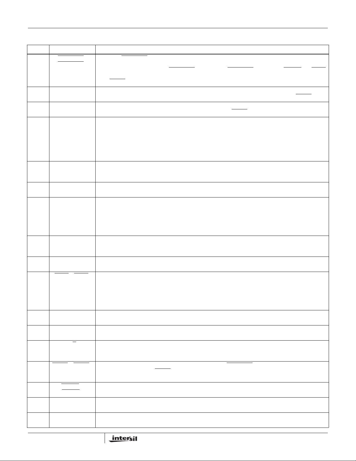
Pin Descriptions
PIN NAME FUNCTION
Asserting a FORCE_ON
9, 28 FORCE_ON
FORCE_ON
44, 43 ONA, ONB Enable input for MAIN outputs use to enable or disable MAIN voltage supply (12V and 3.3V) outputs. Taking ONX
45, 42 AUXENA, AUXENB 3.3VAUX Enable Input, enables the respective VAUX output. Pulling AUXENX low after a fault resets the
5, 32 12VINA,12VINB Connect to 12VMAIN supply and high side of sense resistor. This is one of two pins for Kelvin connection to
8, 29 12VSENSEA,
12VSENSEB
10, 27 12VOUTA,
12VOUTB
12, 25 3VINA, 3VINB Connect to 3VMAIN supply and high side of sense resistor. This provides one of two pins for Kelvin connection to
13, 24 3VSENSEA,
3VSENSEB
16, 21 3VOUTA,
3VOUTB
1, 36 FAULT
15, 22 VAUXA, VA UXB 3.3VAUX output to the PCI-E slot: This output connects to the V AUX pin of the PCI-E connector through an internal
11, 26 VSTBYA
VSTBYB
41 L/R
40, 39 PRSNT
6, 31 PWRGD
PWRGD
4, 38 GPI_A0, GPI_B0 ~5ms debounced user attention input, driven by either a mechanical switch or digital signal form higher level
48, 47 GPO_A0, GPO_B0 User attention output, that can be used to drive LEDs, alarms or other attention getting devices. Open drain with
A,
B
over riding the ON input and the UV, OC and short circuit protections on those outputs. UVLO protection for the
VSTBY input is not affected by the FORCE_ON
outputs to enter their open-drain state. This input is internally pulled high to the VAUX rail. Functionality is disabled
when PRSNT
low after a fault resets the respective slots Main Output Fault Latch. Functionality is disabled when PRSNT
associated slot’s VAUX fault latch. Functionality is disabled when PRSNT
measure the 50mV CR Vth. An undervoltage lockout prevents the IC main supply function until 12VIN >10V . The
current regulation threshold is set by connecting a sense resistor between this pin and 12VSENSE. When the
current-limit threshold of IR = 50mV is reached, the 12VGATE pin is modulated to maintain a constant 50mV
voltage across the sense resistor and thereby a constant current is passed into the load. If the 50mV threshold is
maintained for CR duration, the circuit breaker is tripped and both GATE pins for the affected slot turn off the
switch FETs and thus turn off the supplies to the slot.
12V current sense low side input. This is the second of two pins for Kelvin connection to the R
the 50mV CR Vth. The CR limits are set by connecting a sense resistor between each of these pins and
associated 12VIN pin.
12V output voltage monitor for UV condition. This is the voltage input downstream of the MOSFET that is delivered
to the add-in card load.
measure the 50mV CR Vth. Undervoltage lockout (UVLO) prevents turn-on until 3VIN >2.75V. The current
regulation threshold is set by connecting a sense resistor between this pin and 3VSENSE. When the current-limit
threshold of IR = 50mV is reached, the 3VGATE pin is modulated to maintain a constant 50mV voltage across the
sense resistor and thereby a constant current is passed into the load. If the 50mV threshold is maintained for the
CR duration, the circuit breaker is tripped and both FETs for the affected slot are turned-off.
3.3V current sense low side input. This provides the second of two pins for Kelvin connection for measuring the
50mV CR Vth. The CR limits are set by connecting a sense resistor between each of these pins and associated
3VINX pin.
3.3V output voltage monitor for UV condition. This is the voltage downstream of the MOSFET that is delivered to
the add-in card load.
A, FAULTB An open drain output which is pulled low whenever the CR duration has expired due to an OC fault condition on
A, PRSNTB The card presence detection input disables the operation of the FORCE_ON, ON and AUXEN inputs if not pulled
A,
any of the MAIN or the AUX supplies or in the event of an IC over-temperature condition. If fault latch is invoked
by a MAIN (+12V , +3.3V) supply fault, then it is reset by pulling the faulted slot’s ON pin low . if fault was asserted
because of an OC fault condition on the slot’s AUX output then pulling the AUXEN input low will reset the latch.
Both enabling inputs must be pulled low to clear a fault condition on both the MAIN and VAUX outputs of the same
slot. Internal over-temperature limit is ~+140°C with a +20°C hysteresis.
0.3Ω FET. This output is current regulated to ~1A.
3.3V bias input for the IC, and internal VAUX switches. V
from a dedicated 3.3V or 3VMAIN if AUX supply not implemented.
Latch-off or Retry bar input. Tying this input low invokes a periodic retry to turn-on after current regulation timer
has expired on both slots. Leaving this pin open provides a latch-off operational mode after CR period has expired.
In this mode turn-on is initiated by cycling the appropriate EN input(s). This pin is internally pulled up to VSTBY.
to GND. If after turn-on, the PRSNT
immediately.
A POWER GOOD NOT signal that is asserted low while all output voltages are compliant.
B
controller.
90mA pull-down capability.
is high.
input low will turn on the MAIN and AUX supplies to the respective slot in a forced mode
pins. Asserting FORCE_ON will cause the PWRGD and FAULT
is high.
is high.
to measure
SENSE
must always be present for proper IC bias, either
VSTBY
input goes high then all associated outputs (MAIN and AUX) are turned off
4
FN6457.0
September 25, 2007
Page 5
ISL6113, ISL6114
www.BDTIC.com/Intersil
Pin Descriptions (Continued)
PIN NAME FUNCTION
3, 34 12VGATEA,
14,
23
37, 18 PERST
2, 35 CFILTERA,
17, 33,
46
7,19, 20,
30
12VGATEB
3VGATEA,
3VGATEB
PERST
CFILTERB
GND IC ground reference
NC No Connect
A,
B
12VMAIN gate drive output, connects to gate of an external P-Channel MOSFET. During power-up, this pin is
pulled down with a 25µA (5µA for ISL6114) current to control the dv/dt ramp of the output voltage to the slot. During
CR, the voltage on this pin is modulated to maintain a constant current into the load. During power-down or
latch-off for an overcurrent fault, this pin is pulled high to 12VIN by internal sources.
3VMAIN gate drive outputs connects to gate of an external N-Channel MOSFET . During power-up this pin charges
up with a 25µA (5µA for ISL6114) current to control the dv/dt ramp of the output voltage to the slot load. During
CRTIM the voltage on this pin is modulated to maintain a constant current into the load. During power-down or
latch-off for an overcurrent fault this pin is pulled low by internal sources.
100ms delayed report of MAIN supplies output voltage compliance.
A capacitor connected between each of these pins and ground sets the current regulated duration (tFIL TER) for
each slot. tFILTER is the amount of time for which a slot remains in current limit before its circuit breaker is tripped.
5
FN6457.0
September 25, 2007
Page 6
ISL6113, ISL6114
www.BDTIC.com/Intersil
Absolute Maximum Ratings (Note 3) Thermal Information
12VIN, 12VSENSE, 12VOUT . . . . . . . . . . . . . . . . . . . . . . . . +14.5V
VSTBY, 3VIN, 3VSENSE, 3VOUT. . . . . . . . . . . . . . . . . . . . . . . +7V
12VGATE. . . . . . . . . . . . . . . . . . . . . . . . . . . . . . . . . . . -0.3V to 12VI
3VGATE. . . . . . . . . . . . . . . . . . . . . . . . . . . . . . . . . . . . -0.3V to 12VI
Logic I/O . . . . . . . . . . . . . . . . . . . . . . . . . . . . . . . . . . -0.5V to +5.5V
VAUX Output Current . . . . . . . . . . . . . . . . . .Short Circuit Protected
ESD Rating
Human Body Model . . . . . . . . . . . . . . . . . . . . . . . . . . . . . . . . .2kV
Machine Model. . . . . . . . . . . . . . . . . . . . . . . . . . . . . . . . . . . .200V
Charged Device Model . . . . . . . . . . . . . . . . . . . . . . . . . . . . . .1kV
CAUTION: Do not operate at or near the maximum ratings listed for extended periods of time. Exposure to such conditions may adversely impact product reliability and
result in failures not covered by warranty.
NOTES:
is measured with the component mounted on a high effective thermal conductivity test board in free air. See Tech Brief TB379 for details.
1. θ
JA
2. For θ
3. All voltages are relative to GND, unless otherwise specified.
, the “case temp” location is the center of the exposed metal pad on the package underside.
JC
Thermal Resistance (Typical, N otes 1, 2) θ
48 Ld 7x7 QFN Package . . . . . . . . . . . 27 3
Maximum Junction Temperature . . . . . . . . . . . . . . . . . . . . . . +150°C
Maximum Storage Temperature Range. . . . . . . . . -65°C to +150°C
Pb-free reflow profile . . . . . . . . . . . . . . . . . . . . . . . . . .see link below
http://www.intersil.com/pbfree/Pb-FreeReflow.asp
Operating Conditions
12VMAIN Supply Voltage Range. . . . . . . . . . . . . . . . . . +12V ± 10%
3VMAIN Supply Voltage Range. . . . . . . . . . . . . . . . . . .+3.3V ± 10%
AUXI Supply Voltage Range . . . . . . . . . . . . . . . . . . . . .+3.3V ± 10%
Temperature Range (T
) . . . . . . . . . . . . . . . . . . . . . .-40°C to +85°C
A
(°C/W) θJC (°C/W)
JA
Electrical Specifications 12VIN = 12V, 3VIN and VSTBY = +3.3V, T
PARAMETER SYMBOL TEST CONDITIONS MIN TYP MAX UNIT
MAIN CURRENT REGULATION
Current Limit Threshold Voltages VTHILIMIT V
Fast-Trip Threshold Voltages VTHFAST V
VSENSE Input Current ISENSE 0.1 µA
CFILTER Threshold Voltage VFILTER 1.20 1.25 1.30 V
CFILTER Charging Current
Nominal Current Limit Duration =
x 550k
C
FILTER
AUXILIARY CURRENT REGULATION
Regulated Current Level ILIM(AUX) From end of ISC(TRAN) to
Output MOSFET Resistance VAUX
MOSFET
Off-State Output Offset Voltage VAUX VOFF(VAUX) VAUX = Off, T
BIAS AND POWER GOOD
Supply Current ICC12 Enabled with no load current 0.9 1.5 mA
12VIN, 3VIN, VSTBY Undervoltage
Lockout Thresholds
Undervoltage Lockout Hysteresis
12VIN, 3VIN
IFILTER V
tFILTER CFILTER Open 10 µs
r
ICC3.3 Enabled with no load current 0.1 0.2 mA
ICCSTBY Enabled with no load current 5 6 mA
VUVLO (12V) 12VIN increasing 8 9 10 V
VUVLO (3V) 3VIN increasing 2.1 2.5 2.75 V
VUVLO(STBY) VSTBY increasing 2.8 2.9 2.96 V
VHYSUV 180 mV
DS(AUX)
I
– V
IN
– V
IN
– V
V
IN
– V
VIN
CFILTER time-out
= 375mA, T
DS
= TJ = -40°C to +85°C, Unless Otherwise Specified.
A
47.5 50 52.5 mV
SENSE
(ISL6113) 85 100 115 mV
SENSE
(ISL6114) 140 150 160 mV
SENSE
VSENSE
> V
THILIMIT
2 2.5 3 µA
0.8 1 1.2 A
= +125°C 350 mΩ
J
= +125°C 40 mV
J
6
FN6457.0
September 25, 2007
Page 7
ISL6113, ISL6114
www.BDTIC.com/Intersil
Electrical Specifications 12VIN = 12V, 3VIN and VSTBY = +3.3V, T
PARAMETER SYMBOL TEST CONDITIONS MIN TYP MAX UNIT
Undervoltage Lockout Hysteresis
VSTBY
Power-Good Undervoltage Thresholds VUVTH(12V) 12V
Power-Good Detect Hysteresis VHYSPG 30 mV
GATE DRIVE
12VGATE Voltage VGATE(12V) Max Gate Voltage when Enabled 0 0.55 V
ISL6113 12VGATE Sink Current IGATE (12VSINK) Start Cycle 17 25 35 µA
ISL6114 12VGATE Sink Current Start Cycle 3 5 7 µA
12VGATE Source Current (Fault Off)
(Absolute Value)
3VGATE Voltage VGATE(3V) Min Gate voltage when Enabled 12V
ISL6113 3VGATE Source Current IGATE(3VCHARGE) Start Cycle 17 25 35 µA
ISL6114 3VGATE Source Current Start Cycle 3 5 7 µA
3VGATE Sink Current (Fault Off) IGATE(3VSINK) Any fault condition
ANALOG I/O DC PARAMETERS
GPO Pull-Down Current I
LOW-Level Input Voltage ON, AUXEN,
GPI, FORCE_ON
Output LOW Voltage FAULT
GPO, PERST
HIGH-Level Input Voltage ON, AUXEN,
GPI,FORCE_ON
Internal Pull-ups to VSTBY (Note 4) RPULLUP 40 50 kΩ
12VIN, 3VIN Input Leakage Current ILKG,OFF XVIN VSTBY = +3.3V, 12VIN = OFF;
Input/Output Leakage Current, ON,
AUXEN, GPO, FORCE_ON
Off-State Leakage Current FAULT
PWRGD
Output Discharge Resistance RDIS (12V) 12V
PERST Pull-Down Current when
Asserted.
THERMAL PROTECTION
Over-temperature Shutdown and Reset
Thresholds with Overcurrent on Slot
Over-temperature Shutdown and Reset
Thresholds, all other Conditions (all
Outputs will Latch OFF)
, GPI
, PRSNT
, PWRGD,
, PRSNT
, PERST,
VHYSSTBY 50 mV
OUT
VUVTH(3V) 3V
VUVTH(VAUX) VAUX decreasing 2.55 2.8 3.0 V
IGATE
(12VPULLUP)
GPO_OUT
VIL 0.8 V
VOL IOL = 3mA 0.4 V
VIH 2.1 5 V
IIL -2 2 µA
ILKG(OFF) GPI I
,
RDIS (3V) 3V
RDIS (VAUX) 3VAUX = 1.65V 350 400 Ω
I
PERST
tOVER T
OUT
Any fault condition
(VDD – VGATE) = 2.5V
VGATE = 2.5V
3VIN = OFF
LKG
measured with VAUX OFF
OUT
OUT
ONX is low 30 mA
increasing, each slot 140 °C
J
decreasing, each slot 130 °C
T
J
increasing, both slots 160 °C
T
J
decreasing, both slots 150 °C
T
J
= TJ = -40°C to +85°C, Unless Otherwise Specified. (Continued)
A
decreasing 10.15 10.5 10.75 V
decreasing 2.7 2.8 2.9 V
35 72 mA
for these two pins
- 0.55 12V
IN
80 105 mA
80 mA
0.5 1 µA
-2 2 µA
V
IN
= 6.0V 1400 1850 Ω
= 1.65V 140 180 Ω
7
FN6457.0
September 25, 2007
Page 8
ISL6113, ISL6114
www.BDTIC.com/Intersil
Electrical Specifications 12VIN = 12V, 3VIN and VSTBY = +3.3V, T
PARAMETER SYMBOL TEST CONDITIONS MIN TYP MAX UNIT
I/O TIMING PARAMETERS
12V Current Limit Response Time
3.3V Current Limit Response Time t
VAUX Current Limit Response Time t
Delay from MAIN Overcurrent to FAUL T
output
Delay from VAUX Overcurrent to F AUL T
Output
ON, AUXEN, PRSNT
Power-On Reset Time after VSTBY
Becomes Valid
Auto-Retry Period t
Presence Detect Delay to Auto Enable t
Presence Detect Delay to Disable t
GPI to GPO Propagation Delay t
Delay of Main Power Good to Reporting t
Power Supply Disabled to PERST Low t
NOTE:
4. Limits should be considered typical and are not production tested.
Min Pulse Width t
t
t
or 3V FAULT)
t
t
CGATE = 25pF
OFF(12V)
CGATE = 25pF
OFF(3V)
SC(TRAN)
PROP
PROP
min
POR
RETRY
PRSNT_ON
PRSNT_OFF
GPI-GPO
PVPERL
PERST
VAUX = 0V, VSTBY = +3.3V 2.5 µs
(12V FAULT
(VAUXFAULT) I
100 ns
250 µs
VIN – VSENSE = 140mV
VIN – VSENSE = 140mV
CFILTER = 0
VIN – VSENSE = 140mV
LIM(AUX)
CFILTER = 0 VAUX output
grounded
R/L tied to GND, Any OC Event 0.75 1.4 3 s
PRSNT = high to low 4 6.5 9 ms
PRSNT = low to high 2.5 µs
GPI high/low to GPO high/low 4 6 8 ms
PWRGD low to PERST high. 105 145 185 ms
ON Low to PERST Low 100 ns
to FAULT output
= TJ = -40°C to +85°C, Unless Otherwise Specified. (Continued)
A
1 2.1 µs
0.3 1 µs
1 µs
1 µs
8
FN6457.0
September 25, 2007
Page 9
Typical Application Diagram
www.BDTIC.com/Intersil
ISL6113, ISL6114
100k 100k100k100k
FORCE_ONA
FORCE_ON
B
GPI_A0
GPI_B0
HOT-PLUG
CONTROLLER
PWRGDA
PWRGDB
Float for latch / GND for retry
short pin GND on connector
short pin GND on connector
SYSTEM
POWER
SUPPLY
V
AUXENA
AUXENB
ONA
ONB
FAULTA
FAULTB
10k x 3
STBY
+12V
+3.3V
VSTBY
V
V
VSTBY
C1
STBY
STBY
V
STBY
C2
10k x 4
10k x 4
0.1µF
18
PERSTA
2
CFILTERA
35
CFILTERB
9
FORCE_ON
28
FORCE_ON
4
GPI_A0
38
GPI_B0
45
AUXENA
42
AUXENB
44
ONA
43
ONB
6
PWRGDA
31
PWRGDB
1
FAULTA
36
FAULTB
41
L/R
40
PRSNTA
39
PRSNTB
37
PERSTA
47
GPOB
48
GPOA
11 26
VSTBYBVSTBYA VAUXA
12VSENSEA
A
B
ISL6113
ISL6114
12VSENSEB
0.1µF
12VINA
12VGATEA
12VOUTA
3VINA
3VSENSEA
3VGATEA
3VOUTA
12VINB
12VGATEB
12VOUTB
3VINB
3VSENSEB
3VGATEB
3VOUTB
VAUXB
GND
GND
GND
15
5
8
#C
GS
22nF
3
#C
GD
6800pF
10
12
13
14
16
#
C
GATE
22nF
32
29
#C
22nF
34
27
25
24
23
21
22
17
33
46
0.1µF
*R12VGATEA
0.1 F
*R3VGATEA
0.1µF
GS
0.1µF
15Ω
15Ω
*R12VGATEB
15Ω
#
C
GD
6800pF
*R3VGATEB
15Ω
#CGATE
22nF
PCI-EXPRESS CONNECTOR
PCI
EXPRESS
BUS
RSENSE^
RSENSE^
0.015Ω
RSENSE^
RSENSE^
0.015Ω
3.3AUX
375mA
12V
2.1A (x4/x8)
3.3V
3.0A
12V
2.1A (x4/x8)
3.3V
3.0A
3.3AUX
375mA
PCI
EXPRESS
DATA BUS
* Values for R
depending upon the C
# These components are not required for ISL6113/4
operation but can be implemented for GATE output
slew rate control (application specific)
• Bold lines indicate high current paths
^ R
SENSE
9
PCI-EXPRESS CONNECTOR
12VGATE
value is application specific
and R
3VGATE
of the external MOSFETs.
GS
may vary
FN6457.0
September 25, 2007
Page 10

ISL6113, ISL6114
www.BDTIC.com/Intersil
ISL6113, ISL6114 Descriptions and
Operational Explanation
These two ICs target the dual PCI-EXPRESS slot
application for add-in cards in servers. Together with a pair
of N and P-Channel MOSFETs, four high precision current
sense resistors and a handful of passive components, the
ISL6113, ISL6114 provide a PCI-E compliant hot plug control
solution. These ICs use the Hot Plug Interface (HPI) for
communicating, enabling, monitoring and reporting of UV
conditions and OC and over temperature faults. Additionally
they have a full complement of PCI-E specific I/O.
The ISL6113, ISL6114 share the same footprint as their
sister part, the ISL6112, which features both SMI and HPI
control and communication capabilities, neither of these two
has serial bus capabilities. Whereas the ISL6113 has the
same turn-on characteristics as the ISL6112, the ISL6114
uses a lower level of current sourcing on the GATE outputs
(5µA vs the ISL6113’s 25µA). This lower sourcing current
allows the user to use less GATE capacitance for in-rush
current and GATE ramp control than the ISL6113 to achieve
similar turn-on characteristics. This reduced capacitance in
turn provides for a faster turn-off of the MAIN supplies by the
ISL6114 in the event of an OC fault than is possible with the
ISL6113.
Bias, Power-On Reset and Power Cycling
The ISL6113, ISL6114 utilizes the VSTBY pins as the only IC
bias supply source. For systems without a dedicated 3.3V
auxiliary supply, the 3VMAIN supply is to be used for the IC
bias. A Power-On Reset (POR) cycle is initiated after VSTBY
rises above its UVLO threshold and remains satisfied for
t
, ~250µs. If VSTBY is recycled, the ISL6113, ISL6114
POR
enters a new power-on-reset cycle. VSTBY must be the first
supply voltage applied followed by the MAIN supply inputs.
During t
compliance requires that the connector power must be off
prior to and during insertion and during removal of a PCI-E
board. Before the add-in board is properly inserted into or
removed from a connector, the FET switches are turned off
via the enabling inputs (ON_X and AUXEN_X). In the event
of an improper insertion or removal and to ensure that the
power is off when necessary, the ISL6113, ISL6114 has a
present input (PRSNT
the enabling inputs if PRSNT
card fully inserted into the slot to complete the pull-down
circuit. The PRSNT
connection to ensure compliance.
Enabling the VAUX Outputs
Upon asserting an AUXEN input, the related output turns-on
the internal power switch between the VSTBY supply and its
load. The turn-on is slew rate limited and invokes the ICs
current regulation feature so as to not droop the supply due
to in-rush current loading. Figure 2 illustrates the ISL6113
AUX turn-on performance into a 100Ω, 150µF load with the
in-rush load current being limited to ~1A.
, all outputs remain off. PCI-Express (PCI-E)
POR
) per slot that overrides and disables
is not pulled low by having a
pin must be a last to make, first to break
.
VAUX
AUXEN
IAUX
FIGURE 2. VAUX TURN-ON R
LOAD
= 10Ω, C
LOAD
= 100µF
Standby Mode
Standby mode is entered when one or more of the MAIN
supply inputs (12V
and/or 3VIN) is absent, below its
IN
respective UVLO threshold or OFF. The ISL6113, ISL6114
also has 3.3V auxiliary outputs (VAUX), satisfying an
optional PCI Express requirement. These outputs are fed
from the VSTBY input pins and controlled by the AUXEN
input pins and are independent of the MAIN outputs. Should
IC be in standby mode the V AUX switch will function as long
as V
is compliant. Prior to standby mode, ONA and
VSTBY
ONB inputs must be deasserted or else the ISL6113,
ISL6114 will assert its FAULT
outputs.
Enabling the MAIN GATE Outputs
The related AUXEN must be active for the MAIN supplies to
be enabled otherwise they will be latched off. When a slots
MAIN supplies are off, the 12VGATE pin is held high with an
internal pull-up to the 12VIN voltage. Similarly, the 3VGATE
pin is internally held low to GND. With an add-in card
properly in place, when an ON_X pin is signaled high, the
ISL6113, ISL6114 enables control of one slot turning on one
pair of FETs via the 3VGATE and 12VGATE pins. The FET
gates are charged with a +
25µA (+5µA for the ISL6114)
current sink/source pulling the 12VGATE pin to ground and
the 3VGATE pin is charged to ~12VIN thereby enhancing
both of the MAIN supply FET switches.
Estimating In-Rush Current and V
Slew Rate at
OUT
Start-Up
The expected in-rush current can be estimated by using
Equation 1:
C
⎛⎞
LOAD
ISL6113 - I
ISL6114 - I
Nominally 25μA
INRUSH
Nominally 5μA
INRUSH
=
=
With 25µA and 5µA being the GATE pin charge current for
------------------- -
⎜⎟
C
⎝⎠
GATE
C
⎛⎞
LOAD
------------------- -
⎜⎟
C
⎝⎠
GATE
(EQ. 1)
10
FN6457.0
September 25, 2007
Page 11

ISL6113, ISL6114
www.BDTIC.com/Intersil
the ISL6113, ISL6114 respectively, C
capacitance, and C
including C
of the external MOSFET and any external
ISS
is the total GA TE capacitance
GATE
LOAD
is the load
capacitance connected from the GATE output pin to the
GATE reference, GND or source.
An estimate for the output slew rate of 3.3V outputs and 12V
outputs where there is little or no external 12VGATE output
capacitors, can be taken from Equation 2:
VOUTdv/dt
where I
LIM
LIM
------------------- -
=
C
LOAD
= 50mV/R
SENSE
and C
LOAD
is the load
(EQ. 2)
I
capacitance. Note: As a consequence, the CR duration,
t
must be programmed to exceed the time it takes to
FILTER
fully charge the output load to the input rail voltage level.
MAIN Outputs (Start-up Delay and Slew-Rate
Control)
The 3.3V outputs act as source followers. In this mode of
operation, V
SOURCE
associated output reaches 3.3V. The voltage on the gate of
the MOSFET will then continue to rise until it reaches 12V,
which ensures minimum r
the MOSFET is optionally configured as a Miller integrator to
adjust the V
OUT
connected between the MOSFET’s gate and drain. In this
configuration, the feedback action from drain to gate of the
MOSFET causes the voltage at the drain of the MOSFET to
slew in a linear fashion at a rate estimated by Equation 3:
ISL6113
ISL6114
VOUTdv/dt
VOUTdv/dt
= [V
– V
GATE
. For the 12V outputs, when
DS(ON)
TH(ON)
] until the
ramp time by having a CGD, which is
25μ A
-------------- -
=
C
GD
5μ A
------------
=
C
GD
(EQ. 3)
TABLE 2. ISL6114 3.3V AND 12V OUTPUT SLEW-RA TE
SELECTION FOR GATE CAPACITANCE
DOMINATED START-UP
| IGATE | = 5µA
CGATE or C
0.01µF* 0.5V/ms
0.022µF* 0.23V/ms
0.047µF 0.106 V/ms
0.1µF 0.050V/ms
dv/dt (LOAD)
GD
*Values in this range will be affected by the internal parasitic
capacitances of the MOSFETs used and should be verified
empirically.
During turn-on, the ISL6113 invokes the current regulation
(CR) feature to limit inrush current whereas the ISL6114
disables the CR feature during turn-on thus allowing a
shorter programmed t
or Way Overcurrent (WOC) condition such as a short at this
time.
Note that all of these performance estimates and guidelines
are useful only for first order time and loading expectations,
as they do not look at other significant loading factors.
Figures 3 through 11 realistically illustrate the discussed
turn-on performance topic with the noted loading and
compensation conditions. Notice the degree of control over
the in-rush current and the GATE ramp rate as the C
C
values are changed providing for highly customized
GS
turn on characteristics.
In some scope shots although the C
in the absence of excessive displayed loading current the
C
is responding to the other MAIN supply current that
FILTER
is not displayed.
. Both ICs monitor for a severe
FILTER
shows a ramping
FILTER
GD
and
Tables 1 and 2 approximate the output slew-rate for various
values of C
capacitance (external C
C
of the external MOSFET for the 3.3V rail; CGD for the
GS
when start-up is dominated by GATE
GATE
from GATE pin to ground plus
GATE
12V rail).
TABLE 1. ISL6113 3.3V AND 12V OUTPUT SLEW-RA TE
SELECTION FOR GATE CAPACITANCE
DOMINATED START-UP
| IGATE | = 25µA
CGATE or C
0.01µF* 2.5V/ms
0.022µF* 1.136V/ms
0.047µF 0.532 V/ms
0.1µF 0.250V/ms
*Values in this range will be affected by the internal parasitic
capacitances of the MOSFETs used and should be verified
empirically.
dv/dt (LOAD)
GD
11
All scope shots were taken from the ISL6113EVAL1Z or
ISL6114EVAL1Z platform with any component changes are
noted.
12V
OUT
12V
GATE
12 IOUT
C
FILTER
CGD = 6.8nF
CGS = 22nF
FIGURE 3. ISL6113 12VMAIN START-UP R
= 470µF
C
LOAD
= 10Ω,
LOAD
September 25, 2007
FN6457.0
Page 12

ISL6113, ISL6114
www.BDTIC.com/Intersil
3VGATE
3 V
OUT
12V
OUT
12VGATE
FIGURE 4. ISL6113 3VMAIN ST ART -UP R
= 470µF
C
LOAD
C
GATE
LOAD
C
GD
C
GS
3 IOUT
CFILTER
= 22nF
= 2Ω,
12IOUT
CFILTER
= 6.8nF
= 2.2nF
12V
OUT
12VGATE
FIGURE 7. ISL6113 12VMAIN START-UP R
= 470µF
C
LOAD
= 9.8nF
C
GD
CGS = 2.2nF
= 10Ω,
LOAD
= 1.5nF
C
GD
C
= 4.7nF
GS
12IOUT
CFILTER
12VOUT
12VGATE
12IOUT
CFILTER
FIGURE 5. ISL6113 12VMAIN ST ART-UP R
= 470µF
C
LOAD
FIGURE 6. ISL6113 3VMAIN ST ART -UP R
= 470µF
C
LOAD
12
LOAD
C
GATE
LOAD
= 10Ω,
3VGATE
3V
3IOUT
CFILTER
= 2.2nF
= 2Ω,
OUT
FIGURE 8. ISL6114 12VMAIN START-UP R
= 470µF
C
LOAD
FIGURE 9. ISL6114 3VMAIN START-UP R
= 470µF
C
LOAD
= 10Ω,
LOAD
C
= 4.7nF
GS
= 2Ω,
LOAD
September 25, 2007
3VGATE
3 V
OUT
3 IOUT
3 IOUT
CFILTER
FN6457.0
Page 13

ISL6113, ISL6114
www.BDTIC.com/Intersil
FIGURE 10. ISL6114 12VMAIN START-UP R
= 470µF
C
LOAD
C
C
= OPEN
GD
= OPEN
GS
LOAD
12V
12VGATE
12IOUT
CFILTER
= 10Ω,
3V
GATE
3V
OUT
OUT
ISL61 13, ISL6114 enters its CR mode where it regulates the
load current to the programmed level by modulating the gate of
the related FET switch into the linear region of operation to
maintain 50mV across the sense resistor for the programmed
t
duration. However, should the load current cause a
FILTER
V
RSENSE
no t
ISL61 13, ISL6114 latches off due to the t
> V
delay, as shown in Figures 14 and 15. If the
FILTER
, the outputs are immediately shut off with
THFAST
FILT ER
expiring, then
the FET s are turned-off more aggressively than if signaled from
the linear region with approximately 80mA of GATE current to
ensure faster isolation from the voltage bus. This is also true
when turning of f fr om a WOC e vent .
12V
OUT
12VGATE
12IOUT
C
FILTER
3IOUT
CFILTER
C
= OPEN
GS
FIGURE 11. ISL6114 3VMAIN START-UP R
= 470µF
C
LOAD
LOAD
= 2Ω,
Current Regulation (CR) Function
The ISL6113, ISL6114 provides a current limiting function that
protects the input voltage supplies against excessive current
loads, including short circuits during turn-on (MAIN supplies
shown in previous Figures 3 through 11) and during static
operation for both MAIN (Figures 12 through 15) and AUX
supplies (Figures 16 and 17). When during static operation, any
load current causes >V
THILIMIT
a sense resistor thus exceeding the programmed CR limit, the
(nominally 50mV) drop across
FIGURE 12. ISL6113 12VMAIN CR AND SHUTDOWN
3IOUT
3V
OUT
CFILTER
FIGURE 13. ISL6113 3VMAIN CR AND SHUTDOWN
3VGATE
13
FN6457.0
September 25, 2007
Page 14

ISL6113, ISL6114
www.BDTIC.com/Intersil
12V
OUT
CFILTER
12IOUT
FIGURE 14. ISL6113 12VMAIN WOC SHUTDOWN
3VGATE
CFILTER
12VGATE
VAUX
CFILTER
IAUX
FIGURE 16. VAUX OC REGULATION AND SHUTDOWN
VAUX
CFILTER
3V
3 IOUT
FIGURE 15. ISL6113 3VMAIN WOC SHUTDOWN
OUT
The VAUX outputs have a different circuit-breaker function.
The VAUX circuit breakers do not incorporate a fast-trip
detector, instead they regulate the current into a fault to
avoid exceeding their operating current limit. The circuit
breaker will trip due to an overcurrent on VAUX when the
programmable CR duration timer, t
the t
prematurely due to brief current transients. See Figures 16
timer prevents the circuit breaker from tripping
FLT
expires. This use of
FLT
and 17 for illustrations of the VAUX protection performance
into an over current (OC) and more severe OC condition
respectively. The ISL6113, ISL6114 AUX current control
responds proportionally to the severity of the OC condition
resulting in appropriately fast VAUX pull down and current
regulation until t
FILTER
has expired.
IAUX
FIGURE 17. VAUX WOC REGULATION AND SHUTDOWN
In the fault latch mode set by leaving L/R
pin open, following a
fault condition, the outputs can be turned on ag ain via the ON
inputs (if the fault occurred on one of the MAIN outputs), via
the AUXEN inputs (if the fault occurred on the AUX outputs),
or by cycling both ON and AUXEN (if faults occurred on both
the MAIN and AUX outputs). When the circuit breaker trips,
FAULT
will be asserted. In the fault retry mode, set by
grounding the L/R
pin the ISL611 3, ISL6114 will initiate an
automatic restart about every 1.5s until successful.
The ISL6113, ISL6114 current regulation duration (t
FILTER
)
is set by external capacitors at the CFILTER pins to GND.
Once the CR mode is entered, the external cap is charged
with a 2.5µA current source to 1.25V. Once this threshold
has been reached the IC then turns-off all fault the related
FETs and sets the FAULT
the value for C
C
FILTER
CFILTER
nominal t
--------------------------------------------
=
500kΩ
output low. For a desired t
is given by Equation 4:
FILTER
FILTER
(EQ. 4)
,
14
FN6457.0
September 25, 2007
Page 15

ISL6113, ISL6114
www.BDTIC.com/Intersil
where 500kΩ is (nominal V
where t
I
FILTER
“Electrical Specifications Table” on page6. See Table 3 for
nominal t
For the ISL6113, there is a minimum t
since the ISL6113 has it s CR feature invoked as it turns-on the
FETs into the load. There is a maximum bulk capacitance
specified for each power level supported that needs to be
charged at the CR limit. This in-rush current time must be
considered when programming the t
C
FILTER
NOTE: Nom. CR_DUR =
Holding the CFILTER pin low will increase the CR duration
indefinitely. This feature may be useful in trouble shooting, or
evaluation. If this is invoked be cautious not to violate the
SOA of the pass FETs.
is the desired response time with the values for
FILTER
and V
FILTER
CAPACITANCE (µF) TIME (ms)
Open 0.01
0.022 11
0.047 24
being found in the ISL61 1 3, ISL6114’s
FILTER
times for given C
TABLE 3.
NOMINAL t
0.01 5
0.1 50
C
FILTER
/nominal I
FILTER
FILTER
FILTER
DURATION
FILTER
cap (µF) * 500kΩ.
cap values.
FILTER
.
) and
FILTER
consideration
Power-Down Cycle
When signaled off, the GA TE pins are discharged/charged with
a 25µA for ISL6 113 (5µA for ISL6114) current sink/source to
ramp down the supplies in a controlled fashion. When a slot is
turned off, internal switches are connected to the outputs
12V
capacitance. This ensures that the outputs are pulled to
GND, thereby ensuring 0V on slot connectors during
removal or insertion of add-in cards.
OUT
and 3V
providing a discharge path for load
OUT
Thermal Shutdown
The internal VAUX switches are protected against damage not
only by current limiting, but by a dual mode over-temperature
protection scheme as well. Each slot controller on the ISL6113,
ISL6114 is thermally isolated from the other . Should an
overcurrent condition raise the junction temperature of one
slots controller and pass switch > T
all of the outputs for that slot will be shut off and the slots FAUL T
output will be asserted. The other slots operating condition will
remain unaffected. However, should the ISL61 13, ISL61 14’s die
temperature exceed +160°C, all outputs for both slots will be
shut off, whether or not a current limit condition exists.
(nominally +140°C),
OVER
Special I/O
Power Good Outputs (PWRGD)
The ISL6113, ISL6114 have two open-drain, active-low
PWRGD
output will be asserted when a slot has been enabled and
outputs that must be pulled up to VSTBY. This
the 12VMAIN, 3VMAIN and VAUX outputs exceed their
respective V
UVTH
levels.
PCI-E Reset Outputs (PERST)
A PCI-Express specific output, the ISL6113, ISL6114 have
two open-drain, active-low PERST
pulled up to VSTBY. Upon enabling, the assertion high of
PERST
is delayed a minimum of 100ms (t
power rails achieving minimum specified operating limits for
stability of supplies and REFCLK. Once high the card
functions can safely start-up. PERST
low when the power supply is disabled.
outputs that must be
PVPERL
is immediately pulled
) from the
Force_On Inputs (FORCE_ON)
These inputs are provided to facilitate system diagnostics or
evaluation when using the ISL6113, ISL6114. Asserting a
FORCE_ON
while over riding all three supplies overcurrent, the MAIN
supplies UV protections, on-chip thermal protection for the
VAUX supplies and disable the PWRGD
Asserting the FORCE_ON
V
UVLO(STBY)
VSTBY.
input will turn on all three of the slots outputs,
and FAULT outputs.
inputs will not disable the
. If not used, each pin should be connected to
General Purpose I/O (GPI, GPO)
Two pairs of pins on the ISL6113, ISL6114 are available for
buffered driving. Both of these are compliant to 3.3V. If
unused, connect each GPI pin to GND. The GPI pins are
5ms debounced for filtering and the GPO are open drain
capable of 90mA pull down current for attention getting
devices in accordance with the PCI-Express specifications.
Latch/Retry Operation Toggle (L/R)
This input pin is tied to GND for a ~1.5s retry period after
fault. If left open or tied high to VSTBY , the ISL6113, ISL61 14
will latch off upon a fault.
Board Present Input (PRSNT)
The PRSNT input is used to detect the presence of an add-in
card in the slot. In systems where Manual Retention Latch
(MRL) is not implemented, this input detects when an add-in
card is properly inserted into the slot via the last make,
staggered length PRSNT
connector. This input must be pulled to ground through the addin card ensuring all connections have been made between the
connector and the card in order to enable 3.3VAUX turn-on.
This pin function can be defaulted by tying to GND. PRSNT
being pulled low overrides and disables all FORCE_ON
and AUXEN commands and for ~5ms after being pulled low. In
systems where MRL is implemented this input is connected to
the MRL sensor. The MRL Sensor allows monitoring of the
position of the MRL and therefore allows detection of
unexpected openings of the MRL. These inputs are internally
pulled up to the VSTBY rail. All I/O are valid at VSTBY <1V.
connection on the add-in card
not
, ON
15
FN6457.0
September 25, 2007
Page 16

ISL6113, ISL6114
www.BDTIC.com/Intersil
PCI-Express Application
Recommendations
For each of the 3VMAIN and +12VMAIN supply, the CR level is
set by an external sense resistor value depending on the
maximum specified power for the various sizes of the
PCI-Express connector and application implemented (X1, 10W
or 25W; X4, X8, 25W; X16, 25W or 75W; and X16
Graphic-ATX, 150W). The power rating is a combination of both
main and the optional auxiliary supplies. This sense resistor is a
low sub-1Ω standard value current sense resistor (one for each
slot) and the voltage across this resistor is compared to a 50mV
reference. On the 12VMAIN, for a10W connector, a 75mΩ
sense resistor provides a nominal CR level of 0.66A, 32%
above the 0.5A maximum specification; for a 25W connector, a
20mΩ sense resistor provides a nominal CR level of 2.5A, 19%
above the 2.1A maximum specification; for a 75W connector a
8mΩ sense resistor provides a nominal CR level of 6.25A, 14%
above the 5.5A maximum specification; for a X16 GraphicsAT X 150W card, a 7mΩ sense resistor provides a nominal CR
level of 7.1A, 14% above the 6.25A maximum sp ecificatio n.
The 150W is provided by 2 slots, each providing up to a
maximum of 75W from the 12VMAIN as this specialized type of
card does not consume 3VMAIN or AUX supply power. The
3.3V supply uses a 15mΩ sense resistor compared to a 50mV
reference to provide a nominal CR of 3.3A or 11% above the 3A
maximum specification load across all sizes and power levels
of the connector.
Table 4 provides recommended 12VMAIN sense resistor
values for particular power levels.
TABLE 4.
NOMINAL CURRENT REGULATION LEVEL
12VMAIN R
NOTE: CR Level = VTH
Providing a nominal CR protection level above the maximum
specified limits of the card ensures that the card is able to
draw its maximum specified loads, and, in addition, have
enough headroom before a regulated current limiter is
invoked to protect against transients and other events. This
headroom margin can be adjusted up or down by utilizing
differing values of sense resistor.
SENSE
(mΩ)
75 0.7 10
20 2.5 25
86.2 75
77 150
12VMAIN
CR (A)
ILIMIT/RSENSE
PCI-E ADD IN BOARD POWER
LEVEL SUPPORTED (W)
.
Using the ISL6113EVAL1Z,
ISL6114EVAL1Z Platform
Description and Introduction
The primary ISL61 13, ISL61 14 evaluation plat form is shown in
Figures 37 and 38 both photographically and schematically.
This evaluation board highlights a PCB layout that confines all
necessary active and passive components in an area
12mmx55mm. This width is smaller than the specified
PCI-Express socket to socket spacing allowing for intima te
co-location of the load power control and the load itself.
Around the central highlighted layout are numerous labeled
test points and configuration jumpers. Where there are node
names such as, AO(L/R
relates to the ISL6113, ISL6114. The ISL6113, ISL6114
share an evaluation platform with the ISL6112 as all three
parts have a common pinout for the common pin functions.
The specific evaluation board as ordered and received will
reflect the part number in the area below the Intersil logo
either by label or silk screened lettering. For those pins not
common across the ISL6112 and ISL6113, ISL6114 in the
bottom left corner there is a matrix detailing the differences.
After correctly biasing the evaluation platform as noted
through the 6 banana jacks, turning on VSTBY first then the
other MAIN supplies in any order. With the appropriate
signaling to the AUXEN and ON inputs the user should see
turn-on waveforms as shown previously. The addition of
external current loading is necessary to demonstrate the OC
and WOC response performance.
Figures 18 and 19 demonstrate some of the PCI-E specific
and additional I/O functionality. Figure 18 shows the PRSNT
pin being signaled low then the 12V
turning on automatically as the ON input is already asserted.
Power good is signaled once the 12V
their respective VUVVth levels. Af ter the time period t
the PCI-E specific reset signal output, PERST is asserted.
Figure 19 shows the GPI to GPO ~6ms functionality.
Figure 20 shows the retry period operation. Approximately
every 1.5s the IC attempts to restart into a faulty load until
finally being able to turn-on fully into a normal load. This retry
mode is invoked with R
ISL6113EVAL1Z, ISL6114EVAL1Z Errata
GPO_A0 and GPO_BO labeling is reversed. Correct
labeling shown on evaluation board photograph in Figure 37.
Caution: The ISL6113EVAL1Z, ISL6114EVAL1Z gets very
hot to the touch after operating it for a few minutes. Hottest
areas marked on evaluation board.
) the pin name in parentheses
and 3V
OUT
OUT
/L input tied low.
and 3V
OUT
OUT
outputs
meet
PVPERL
16
FN6457.0
September 25, 2007
Page 17

PRSNT
www.BDTIC.com/Intersil
PGOOD
12VOUT
3V
OUT
t
PVPERL
ISL6113, ISL6114
GPO
GPI
PERST
FIGURE 18. PRSNT, V
, POWERGOOD, PERST
OUT
FIGURE 19. GPI TO GPO FUNCTIONALITY
12VMAIN
3VMAIN
12GATE
12IOUT
FIGURE 20. RETRY MODE OPERATION
17
FN6457.0
September 25, 2007
Page 18

Typical Performance Curves
www.BDTIC.com/Intersil
ISL6113, ISL6114
6.0
5.8
5.6
5.4
5.2
5.0
4.8
ICCSTBY (mA)
4.6
4.4
4.2
4.0
-60 -40 -20 0 20 40 60 80 100 120
TEMPERATURE (°C)
FIGURE 21. ICCSTBY CURRENT vs TEMPERATURE
53
52
51
50
49
48
CURRENT LIMIT Vth (mV)
47
-60 -40 -20 0 20 40 60 80 100 120
TEMPERATURE (°C)
FIGURE 23. CURRENT LIMIT THRESHOLD VOL T AGE
vs TEMPERATURE
1.0
0.8
0.6
0.4
ICC (mA)
0.2
0
-50 0 50 100 150
12V ICC
3.3V ICC
TEMPERATURE (°C)
FIGURE 22. ICC CURRENT vs TEMPERATURE
104
103
102
101
100
99
98
97
WOC THRESHOLD VOLTAGE (V)
96
-60 -40 -20 0 20 40 60 80 100 120
TEMPERATURE (°C)
FIGURE 24. FAST TRIP THRESHOLD VOLT A GE
vs TEMPERATURE
1200
1150
1100
1050
1000
950
900
850
AUX CURRENT LIMIT (mA)
800
-60 -40 -20 0 20 40 60 80 100 120
TEMPERATURE (°C)
FIGURE 25. AUX CURRENT LIMIT vs TEMPERATURE
400
380
360
340
320
300
280
260
240
AUX RESISTANCE (Ω)
220
200
-60 -40 -20 0 20 40 60 80 100 120
FIGURE 26. AUX r
18
IAUX = 375mA
TEMPERATURE (°C)
vs TEMPERATURE
DS(ON)
FN6457.0
September 25, 2007
Page 19

Typical Performance Curves (Continued)
www.BDTIC.com/Intersil
ISL6113, ISL6114
9.30
9.25
9.20
9.15
9.10
12VMAIN POR RISING (V)
9.05
-60 -40 -20 0 20 40 60 80 100 120
TEMPERATURE (°C)
FIGURE 27. 12VMAIN RISING POR THRESHOLD VOLT AGE
vs TEMPERATURE
10.54
10.52
10.50
10.48
10.46
10.44
10.42
12VMAIN UV Vth (V)
10.40
10.38
-60 -40 -20 0 20 40 60 80 100 120
TEMPERATURE (°C)
FIGURE 29. 12VMAIN POWER GOOD THRESHOLD VOL T AGE
vs TEMPERATURE
3.1
2.9
2.7
2.5
2.3
2.1
1.9
1.7
AUX AND 3VMAIN RISING POR (V)
1.5
-60 -40 -20 0 20 40 60 80 100 120
AUX
3VMAIN
TEMPERATURE (°C)
FIGURE 28. AUX AND 3VMAIN RISING POR THRESHOLD
VOLTAGE vs TEMPERATURE
2.80
2.79
2.78
2.77
2.76
2.75
2.74
2.73
2.72
AUX AND 3VMAIN UV Vth (V)
2.71
2.70
-60 -40 -20 0 20 40 60 80 100 120
AUX
TEMPERATURE (°C)
3VMAIN
FIGURE 30. AUX AND 3VMAIN POWER GOOD THRESHOLD
VOLTAGE vs TEMPERATURE
25.5
25.0
24.5
T (µA)
24.0
23.5
23.0
22.5
TURN ON CURREN
22.0
-60 -40 -20 0 20 40 60 80 100 120
3V
GATE
12V
TEMPERATURE (°C)
GATE
FIGURE 31. ISL6113 GATE TUR N-ON CURRENT (ABS)
5.1
5.0
4.9
4.8
4.7
4.6
4.5
TURN ON CURRENT (µA)
4.4
-60 -40 -20 0 20 40 60 80 100 120
FIGURE 32. ISL6114 GATE TUR N-ON CURRENT (ABS)
vs TEMPERATURE
19
3V
GATE
TEMPERATURE (°C)
vs TEMPERATURE
12V
GATE
FN6457.0
September 25, 2007
Page 20

Typical Performance Curves (Continued)
www.BDTIC.com/Intersil
ISL6113, ISL6114
120
100
80
60
40
20
GATE FAULT OFF CURRENT (mA)
0
-60 -40 -20 0 20 40 60 80 100 120
TEMPERATURE (°C)
3GATE
12GATE
FIGURE 33. GATE FAULT OFF CURRENT (ABS)
3.0
2.9
2.8
2.7
2.6
2.5
2.4
2.3
2.2
FILTER CURRENT (µA)
2.1
2.0
-60 -40 -20 0 20 40 60 80 100 120
FIGURE 34. FILTER CHARGE CURRENT vs TEMPERA TURE
vs TEMPERATURE
1.30
1.28
1.26
1.24
1.22
FILTER THRESHOLD (V)
1.20
-60 -40 -20 0 20 40 60 80 100 120
TEMPERATURE (°C)
160
155
150
145
PVPERL (ms)
t
140
135
130
-60 -40 -20 0 20 40 60 80 100 120
FIGURE 35. FILTER THRESHOLD VOLTAGE vs TEMPERATURE FIGURE 36. t
TEMPERATURE (°C)
TEMPERATURE (°C)
vs TEMPERATURE
PVPERL
20
FN6457.0
September 25, 2007
Page 21
CAUTION HOT AREA
www.BDTIC.com/Intersil
ISL6113, ISL6114
GPO_A
GPO_B
CAUTION HOT AREA
CAUTION HOT AREA
FIGURE 37. ISL6113EVAL1Z, ISL6114EVAL1Z BOARD PHOTOGRAPH
21
FN6457.0
September 25, 2007
Page 22

22
www.BDTIC.com/Intersil
ISL6113
ISL6114
September 25, 2007
FN6457.0
ISL6113, ISL6114
FIGURE 38. ISL6113EVAL1Z, ISL6114EVAL1Z BOARD SCHEMATIC
Page 23

ISL6113, ISL6114
www.BDTIC.com/Intersil
TABLE 5. ISL6113EVAL1Z, ISL6114EVAL1Z COMPONENT LISTING
COMPONENT
DESIGNATOR COMPONENT FUNCTION COMPONENT DESCRIPTION
U1 ISL6113 or ISL6114 PCI-Express Dual Slot Hot Plug Controller
Q1, Q4 Voltage Rail Switches SI4405DY or equivalent, P-Channel MOSFET
Q2, Q3 Voltage Rail Switches SI4820DY or equivalent, N-Channel MOSFET
R1, R3, R6, R8 Current Sense Resistor 0.020Ω 1%, 2512
R9, R10, R17, R20 Pull-up resistors on FORCE_ON
R11, R12, R13, 14,
R15, R16, R18, 19,
R21
R2, R4, R5, R7 FET gate series resistance 15Ω, 0201
C1, C7, C8, C13 ISL6113EVAL1Z 3VMAIN FET gate capacitance 22nF 10%, 16V, 0402
C1, C7, C8, C13 ISL6114EVAL1Z 3VMAIN FET gate capacitance open
C3, C5, C6, C10,
C11, C14
C2, C12 ISL6113 12VMAIN FET gate to drain capacitance 6.8nF 10%, 6.3V, 0201
C2, C12 ISL6114 12VMAIN FET gate to drain capacitance open
C4, C9
R24, R25 AUX Load Resistance 10Ω 20%, 3W
C17, C18 AUX Load Capacitance 100µF 20%, 25V, Radial Electrolytic
R22, R26, R28, 29 12VMAIN Load Resistance 20Ω 20%, 10W
R23, R27 3VMAIN Load Resistance 2Ω 20%, 10W
C15, C16, C19, C20 12VMAIN and 3VMAIN Load Capacitance 470µF 20%, 16V, Radial Electrolytic
I/O Pull-up resistors 10kΩ, 0201
MAIN and VSTBY decoupling capacitance 1µF 10%, 6.3V, 0402
C
capacitance (5ms) 0.01µF 10%, 6.3V, 0201
FILTER
and GPI Inputs 100kΩ, 0201
All Intersil U.S. products are manufactured, assembled and tested utilizing ISO9000 quality systems.
Intersil Corporation’s quality certifications can be viewed at www.intersil.com/design/quality
Intersil products are sold by description only. Intersil Corporation reserves the right to make changes in circuit design, software and/or specifications at any time without
notice. Accordingly, the reader is cautioned to verify that data sheets are current before placing orders. Information furnished by Intersil is believed to be accurate and
reliable. However, no responsibility is assumed by Intersil or its subsidiaries for its use; nor for any infringements of patents or other rights of third parties which may result
from its use. No license is granted by implic atio n or other wise u nde r any p a tent or patent rights of Intersil or its subsidiaries.
For information regarding Intersil Corporation and its products, see www.intersil.com
23
FN6457.0
September 25, 2007
Page 24

Package Outline Drawing
www.BDTIC.com/Intersil
L48.7x7
48 LEAD QUAD FLAT NO-LEAD PLASTIC PACKAGE
Rev 4, 10/06
7.00
6
PIN 1
INDEX AREA
ISL6113, ISL6114
A
B
37
36
4X
44X
5.5
0.50
48
6
PIN #1 INDEX AREA
1
(4X) 0.15
( 6 . 80 TYP )
( 4 . 30 )
TOP VIEW
TYPICAL RECOMMENDED LAND PATTERN
7.00
0 . 90 ± 0 . 1
( 44X 0 . 5 )
( 48X 0 . 23 )
( 48X 0 . 60 )
25
24
48X 0 . 40± 0 . 1
BOTTOM VIEW
SIDE VIEW
0 . 2 REF
C
DETAIL "X"
0 . 00 MIN.
0 . 05 MAX.
12
13
4
0.23 +0.07 / -0.05
BASE PLANE
5
4. 30 ± 0 . 15
M0.10 C AB
SEE DETAIL "X"
C
C
0.10
SEATING PLANE
C0.08
NOTES:
Dimensions are in millimeters.1.
Dimensions in ( ) for Reference Only.
Dimensioning and tolerancing conform to AMSE Y14.5m-1994.
2.
3.
Unless otherwise specified, tolerance : Decimal ± 0.05
Dimension b applies to the metallized terminal and is measured
4.
between 0.15mm and 0.30mm from the terminal tip.
Tiebar shown (if present) is a non-functional feature.
5.
The configuration of the pin #1 identifier is optional, but must be
6.
located within the zone indicated. The pin #1 indentifier may be
either a mold or mark feature.
24
FN6457.0
September 25, 2007
 Loading...