

Page 1
查询ISL60002BAH333Z-TK供应商
®
ISL60002
Data Sheet January 5, 2006
Precision Low Power FGA™ Voltage
References
The ISL60002 FGA™ voltage references are very high
precision analog voltage references fabricated in Intersil's
proprietary Floating Gate Analog technology and feature low
supply voltage operation at ultra-low 400nA operating
current.
Additional features include guaranteed initial accuracy as
low as ±1.0mV, @ 20ppm/°C temperature coefficient and
long-term stability of <<10ppm/√1kHrs
and thermal stability performance of the ISL60002 family
plus the low supply voltage and 400nA power consumption
eliminates the need to compromise thermal stability for
reduced power consumption making it an ideal companion to
high resolution, low power data conversion systems.
. The initial accuracy
FN8082.3
Features
• Reference Voltages . .1.024V, 1.2V, 1.25V, 1.8V, 2.5V and
3.3V
• Absolute Initial Accuracy Options. . . ±1.0mV, ±2.5mV, and
±5.0mV
• Supply Voltage Range
- ISL60002-10, -11, -12, -18, -20, -25 . . . . . . 2.7V to 5.5V
- ISL60002-33 . . . . . . . . . . . . . . . . . . . . . . . . 3.5V to 5.5V
• Ultra-Low Supply Current. . . . . . . . . . . . . . . . . . 350nA typ
• Low 20ppm/°C Temperature Coefficient
• 10ppm/√1kHrs
•I
SOURCE
•I
SOURCE
• ESD Protection. . . . . . . . . . . . . 5kV (Human Body Model)
• Standard 8 Ld SOIC and 3 Ld SOT-23 Packaging
• operating Temperature Range
- ISL60002-10, -11, -12, -18, -20, -25 . . . .-40°C to +85°C
- ISL60002-33 . . . . . . . . . . . . . . . . . . . . .-40°C to +105°C
• Pb-Free Plus Anneal Available (RoHS Compliant)
. Long Term Stability
and I
and I
= 7mA
SINK
= 20mA for ISL60002-33 only
SINK
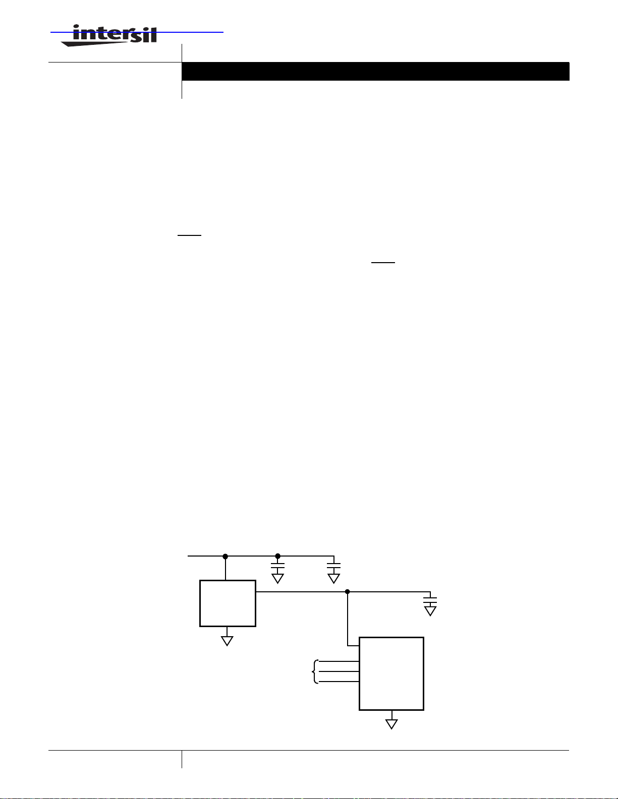
Typical Application
VIN = +3.0V
*Also see Figure 103 in Applications Information.
V
IN
V
ISL60002
GND
OUT
0.1µF
Serial
Bus
Applications
• High Resolution A/Ds and D/As
• Digital Meters
• Bar Code Scanners
• Mobile Communications
• PDA’s and Notebooks
• Medical Systems
10µF
0.001µF
REF IN
ENABLE
SCK
SDAT
16 TO 24-BIT
A/D CONVERTER
*
1
CAUTION: These devices are sensitive to electrostatic discharge; follow proper IC Handling Procedures.
1-888-INTERSIL or 1-888-468-3774
FGA is a trademark of Intersil Corporation. Copyright Intersil Americas Inc. 2004-2006. All Rights Reserved
| Intersil (and design) is a registered trademark of Intersil Americas Inc.
All other trademarks mentioned are the property of their respective owners.
Page 2

ISL60002
Table of Contents
Typical Application......................................................................................................................................................................... 1
Pinouts .......................................................................................................................................................................................... 3
Pin Descriptions ............................................................................................................................................................................ 3
Ordering Information ..................................................................................................................................................................... 3
Absolute Maximum Ratings........................................................................................................................................................... 5
Electrical Specifications
ISL60002-10, VOUT = 1.024V ................................................................................................................................................. 5
ISL60002-11, V
ISL60002-12, V
ISL60002-18, V
ISL60002-20, V
ISL60002-25, V
ISL60002-33, V
Common Electrical Specifications
ISL60002-10, -11, -12, -18, -20, and -25.................................................................................................................................. 7
Typical Performance Characteristic Curves
ISL60002, V
ISL60002, V
ISL60002, V
ISL60002, V
ISL60002, V
ISL60002, V
ISL60002, V
Applications Information................................................................................................................................................................ 27
= 1.200V .................................................................................................................................................. 5
OUT
= 1.250V .................................................................................................................................................. 5
OUT
= 1.800V .................................................................................................................................................. 6
OUT
= 2.048V .................................................................................................................................................. 6
OUT
= 2.500V .................................................................................................................................................. 6
OUT
= 3.300V .................................................................................................................................................. 6
OUT
= 1.024V ....................................................................................................................................................... 8
OUT
= 1.20V ......................................................................................................................................................... 10
OUT
= 1.25V ......................................................................................................................................................... 13
OUT
= 1.8V ........................................................................................................................................................... 16
OUT
= 2.048V ....................................................................................................................................................... 18
OUT
= 2.50V ......................................................................................................................................................... 21
OUT
= 3.3V ........................................................................................................................................................... 24
OUT
Typical Application Circuits............................................................................................................................................................ 29
Packaging Information................................................................................................................................................................... 30
2
Page 3
ISL60002
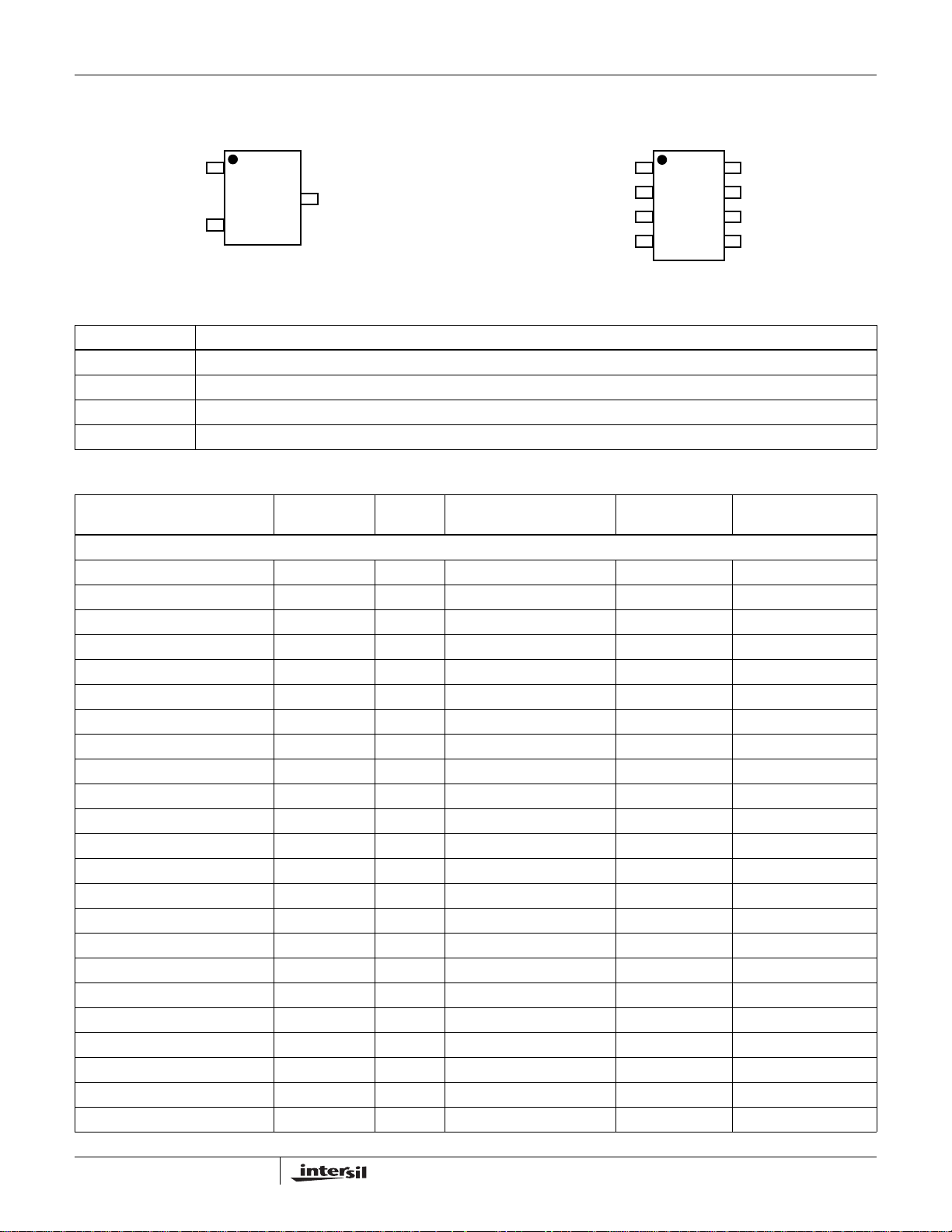
Pinouts
ISL60002 (SOT-23-3)
TOP VIEW
1
V
IN
V
2
OUT
3
GND
ISL60002 (SOIC-8)
TOP VIEW
1
GND
V
2
IN
3
DNC
GND
4
8
DNC
7
DNC
6
V
OUT
5
DNC
Pin Descriptions
PIN NAME DESCRIPTION
GND Ground Connection
V
V
IN
OUT
Power Supply Input Connection
Voltage Reference Output Connection
DNC Do Not Connect; Internal Connection – Must Be Left Floating
Ordering Information
PART
PART NUMBER
MARKING V
(V) GRADE
OUT
3 LD SOT-23
ISL60002BIH310Z-TK (Note) 1.024 ±1.0mV, 20ppm/°C -40 to 85 3 Ld SOT-23 (Pb-free)
ISL60002CIH310Z-TK (Note) 1.024 ±2.5mV, 20ppm/°C -40 to 85 3 Ld SOT-23 (Pb-free)
ISL60002DIH310Z-TK (Note) 1.024 ±5.0mV, 20ppm/°C -40 to 85 3 Ld SOT-23 (Pb-free)
ISL60002BIH311Z-TK (Note) APH 1.200 ±1.0mV, 20ppm/°C -40 to 85 3 Ld SOT-23 (Pb-free)
ISL60002CIH311Z-TK (Note) AOH 1.200 ±2.5mV, 20ppm/°C -40 to 85 3 Ld SOT-23 (Pb-free)
ISL60002DIH311Z-TK (Note) AOY 1.200 ±5.0mV, 20ppm/°C -40 to 85 3 Ld SOT-23 (Pb-free)
ISL60002BIH312-TK AIL 1.250 ±1.0mV, 20ppm/°C -40 to 85 3 Ld SOT-23
ISL60002BIH312Z-TK (Note) 1.250 ±1.0mV, 20ppm/°C -40 to 85 3 Ld SOT-23 (Pb-free)
ISL60002CIH312-TK AIN 1.250 ±2.5mV, 20ppm/°C -40 to 85 3 Ld SOT-23
ISL60002CIH312Z-TK (Note) 1.250 ±2.5mV, 20ppm/°C -40 to 85 3 Ld SOT-23 (Pb-free)
ISL60002DIH312-TK AIP 1.250 ±5.0mV, 20ppm/°C -40 to 85 3 Ld SOT-23
ISL60002DIH312Z-TK (Note) 1.250 ±5.0mV, 20ppm/°C -40 to 85 3 Ld SOT-23 (Pb-free)
ISL60002BIH318Z-TK (Note) 1.800 ±1.0mV, 20ppm/°C -40 to 85 3 Ld SOT-23 (Pb-free)
ISL60002CIH318Z-TK (Note) 1.800 ±2.5mV, 20ppm/°C -40 to 85 3 Ld SOT-23 (Pb-free)
ISL60002DIH318Z-TK (Note) 1.800 ±5.0mV, 20ppm/°C -40 to 85 3 Ld SOT-23 (Pb-free)
ISL60002BIH320Z-TK (Note) 2.048 ±1.0mV, 20ppm/°C -40 to 85 3 Ld SOT-23 (Pb-free)
ISL60002CIH320Z-TK (Note) 2.048 ±2.5mV, 20ppm/°C -40 to 85 3 Ld SOT-23 (Pb-free)
ISL60002DIH320Z-TK (Note) 2.048 ±5.0mV, 20ppm/°C -40 to 85 3 Ld SOT-23 (Pb-free)
ISL60002BIH325-TK AIK 2.500 ±1.0mV, 20ppm/°C -40 to 85 3 Ld SOT-23
ISL60002BIH325Z-TK (Note) 2.500 ±1.0mV, 20ppm/°C -40 to 85 3 Ld SOT-23 (Pb-free)
ISL60002CIH325-TK AIM 2.500 ±2.5mV, 20ppm/°C -40 to 85 3 Ld SOT-23
ISL60002CIH325Z-TK (Note) 2.500 ±2.5mV, 20ppm/°C -40 to 85 3 Ld SOT-23 (Pb-free)
ISL60002DIH325-TK AIO 2.500 ±5.0mV, 20ppm/°C -40 to 85 3 Ld SOT-23
TEMP.
RANGE (°C) PACKAGE
3
Page 4
Ordering Information (Continued)
ISL60002
PART
PART NUMBER
ISL60002DIH325Z-TK (Note) 2.500V ±5.0mV, 20ppm/°C -40 to 85 3 Ld SOT-23 (Pb-free)
ISL60002BAH333Z-TK (Note) AOP 3.300V ±1.0mV, 20ppm/°C -40 to 105 3 Ld SOT-23 (Pb-free)
ISL60002CAH333Z-TK (Note) AOU 3.300V ±2.5mV, 20ppm/°C -40 to 105 3 Ld SOT-23 (Pb-free)
ISL60002DAH333Z-TK (Note) APC 3.300V ±5.0mV, 20ppm/°C -40 to 105 3 Ld SOT-23 (Pb-free)
8 LD SOIC
ISL60002BIB812* 60002BI 12 1.250V ±1.0mV, 20ppm/°C -40 to 85 8 Ld SOIC
ISL60002CIB812* 60002CI 12 1.250V ±2.5mV, 20ppm/°C -40 to 85 8 Ld SOIC
ISL60002DIB812* 60002DI 12 1.250V ±5.0mV, 20ppm/°C -40 to 85 8 Ld SOIC
ISL60002BIB825* 60002BI 25 2.500V ±1.0mV, 20ppm/°C -40 to 85 8 Ld SOIC
ISL60002CIB825* 60002CI 25 2.500V ±2.5mV, 20ppm/°C -40 to 85 8 Ld SOIC
ISL60002DIB825* 60002DI 25 2.500V ±5.0mV, 20ppm/°C -40 to 85 8 Ld SOIC
*Add "TK" suffix for tape and reel.
NOTE: Intersil Pb-free plus anneal products employ special Pb-free material sets; molding compounds/die attach materials and 100% matte tin plate
termination finish, which are RoHS compliant and compatible with both SnPb and Pb-free soldering operations. Intersil Pb-free products are MSL
classified at Pb-free peak reflow temperatures that meet or exceed the Pb-free requirements of IPC/JEDEC J STD-020.
MARKING V
(V) GRADE
OUT
TEMP.
RANGE (°C) PACKAGE
4
Page 5
ISL60002
Absolute Maximum Ratings Recommended Operating Conditions
Storage Temperature Range . . . . . . . . . . . . . . . . . -65°C to + 150°C
Max Voltage V
Max Voltage V
ISL60002, V
ISL60002, V
Voltage on “DNC” pins . . . . No connections permitted to these pins.
to Gnd. . . . . . . . . . . . . . . . . . . . . . . -0.5V to +6.5V
IN
to Gnd*:
OUT
= 1.25V. . . . . . . . . . . . . . . . . . . . . -0.5V to +2.25V
OUT
= 2.50V. . . . . . . . . . . . . . . . . . . . . -0.5V to +3.50V
OUT
Lead Temperature, Soldering* . . . . . . . . . . . . . . . . . . . . . . . .+225°C
*Maximum duration = 10s
CAUTION: Absolute Maximum Ratings are limits which may result in impaired reliability and/or permanent damage to the device. These are stress ratings provided for
information only and functional operation of the device at these or any other conditions beyond those indicated in the operational sections of this specification are not
implied.
For guaranteed specifications and test conditions, see Electrical Specifications.
The guaranteed specifications apply only for the test conditions listed. Some performance characteristics may degrade when the device is not operated under the listed
test conditions.
Temperature Range (Industrial) . . . . . . . . . . . . . . . . . .-40°C to 85°C
ESD Ratings
MIL-STD-883, Method 3014. . . . . . . . . . . . . . . . . . . . . . . . . . . . . . .≥5kV
Electrical Specifications ISL60002-10, V
Operating Conditions: V
= 3.0V, I
IN
OUT
= 0mA, C
OUT
= 1.024V (Additional specifications on page 7, “Common Electrical Specifications”)
OUT
= 0.001µF, TA= -40 to +85°C, unless otherwise specified.
SYMBOL PARAMETER CONDITIONS MIN TYP MAX UNITS
V
OUT
V
OA
Output Voltage 1.024 V
V
Accuracy TA = 25°C
OUT
ISL60002B10 -1.0 +1.0 mV
ISL60002C10 -2.5 +2.5 mV
ISL60002D10 -5.0 +5.0 mV
V
IN
Electrical Specifications ISL60002-11, V
Operating Conditions: V
Input Voltage Range 2.7 5.5 V
= 1.200V (Additional specifications on page 7, “Common Electrical Specifications”)
= 3.0V, I
IN
OUT
= 0mA, C
OUT
= 0.001µF, TA= -40 to +85°C, unless otherwise specified.
OUT
SYMBOL PARAMETER CONDITIONS MIN TYP MAX UNITS
V
OUT
V
OA
Output Voltage 1.200 V
V
Accuracy TA = 25°C
OUT
ISL60002B11 -1.0 +1.0 mV
ISL60002C11 -2.5 +2.5 mV
ISL60002D11 -5.0 +5.0 mV
V
IN
Input Voltage Range 2.7 5.5 V
Electrical Specifications ISL60002-12, V
Operating Conditions: V
= 3.0V, I
IN
OUT
= 0mA, C
OUT
= 1.250V (Additional specifications on page 7, “Common Electrical Specifications”)
OUT
= 0.001µF, TA= -40 to +85°C, unless otherwise specified.
SYMBOL PARAMETER CONDITIONS MIN TYP MAX UNITS
V
OUT
V
OA
Output Voltage 1.250 V
V
Accuracy TA = 25°C
OUT
ISL60002B12 -1.0 +1.0 mV
ISL60002C12 -2.5 +2.5 mV
ISL60002D12 -5.0 +5.0 mV
V
IN
Input Voltage Range 2.7 5.5 V
5
Page 6
ISL60002
Electrical Specifications ISL60002-18, V
Operating Conditions: V
= 3.0V, I
IN
OUT
= 0mA, C
OUT
= 1.800V (Additional specifications on page 7, “Common Electrical Specifications”)
OUT
= 0.001µF, TA= -40 to +85°C, unless otherwise specified.
SYMBOL PARAMETER CONDITIONS MIN TYP MAX UNITS
V
OUT
V
OA
Output Voltage 1.800 V
V
Accuracy TA = 25°C
OUT
ISL60002B18 -1.0 +1.0 mV
ISL60002C18 -2.5 +2.5 mV
ISL60002D18 -5.0 +5.0 mV
V
IN
Electrical Specifications ISL60002-20, V
Operating Conditions: V
Input Voltage Range 2.7 5.5 V
= 2.048V (Additional specifications on page 7, “Common Electrical Specifications”)
= 3.0V, I
IN
OUT
= 0mA, C
OUT
= 0.001µF, TA= -40 to +85°C, unless otherwise specified.
OUT
SYMBOL PARAMETER CONDITIONS MIN TYP MAX UNITS
V
OUT
V
OA
Output Voltage 2.048 V
V
Accuracy TA = 25°C
OUT
ISL60002B20 -1.0 +1.0 mV
ISL60002C20 -2.5 +2.5 mV
ISL60002D20 -5.0 +5.0 mV
V
IN
Input Voltage Range 2.7 5.5 V
Electrical Specifications ISL60002-25, V
Operating Conditions: V
= 3.0V, I
IN
OUT
= 0mA, C
OUT
= 2.500V (Additional specifications on page 7, “Common Electrical Specifications”)
OUT
= 0.001µF, TA= -40 to +85°C, unless otherwise specified.
SYMBOL PARAMETER CONDITIONS MIN TYP MAX UNITS
V
OUT
V
OA
Output Voltage 2.500 V
V
Accuracy TA = 25°C
OUT
ISL60002B25 -1.0 +1.0 mV
ISL60002C25 -2.5 +2.5 mV
ISL60002D25 -5.0 +5.0 mV
V
IN
Electrical Specifications ISL60002-33, V
Operating Conditions: VIN = 5.0V, I
Input Voltage Range 2.7 5.5 V
= 3.300V
OUT
= 0.001µF, TA= -40 to +105°C, unless otherwise specified.
OUT
OUT
= 0mA, C
SYMBOL PARAMETER CONDITIONS MIN TYP MAX UNITS
V
OUT
V
OA
Output Voltage 3.300 V
V
Accuracy TA = 25°C
OUT
ISL60002B33 -1.0 1.0 mV
ISL60002C33 -2.5 2.5 mV
ISL60002D33 -5.0 5.0 mV
∆V
∆V
TC V
OUT
OUT
OUT
V
IN
I
IN
/∆V
/∆I
Output Voltage Temperature
Coefficient (Note 1)
Input Voltage Range 3.5 5.5 V
Supply Current 350 700 nA
Line Regulation +3.5V ≤ VIN ≤ +5.5V 80 200 µV/V
IN
Load Regulation 0mA ≤ I
OUT
SOURCE
-20mA ≤ I
≤ 20mA 25 100 µV/mA
≤ 0mA 50 150 µV/mA
SINK
20 ppm/°C
6
Page 7
ISL60002
Electrical Specifications ISL60002-33, V
Operating Conditions: V
= 5.0V, I
IN
OUT
= 0mA, C
OUT
= 3.300V (Continued)
OUT
= 0.001µF, TA= -40 to +105°C, unless otherwise specified.
SYMBOL PARAMETER CONDITIONS MIN TYP MAX UNITS
∆V
/∆t Long Term Stability (Note 4) TA = 25°C 10 ppm/√1
OUT
kHrs
∆V
OUT
I
SC
V
/∆T
N
Thermal Hysteresis (Note 2) ∆TA = 145°C 100 ppm
A
Short Circuit Current (Note 3) TA = 25°C 50 80 mA
Output Voltage Noise 0.1Hz ≤ f ≤ 10Hz 30 µV
P-P
Common Electrical Specifications ISL60002-10, -11, -12, -18, -20, and -25
Operating Conditions: VIN = 3.0V, I
SYMBOL PARAMETER CONDITIONS MIN TYP MAX UNITS
∆V
∆V
TC V
OUT
I
IN
/∆V
OUT
/∆I
OUT
∆V
/∆t Long Term Stability (Note 4) TA = 25°C 10 ppm/√1
OUT
∆V
/∆T
OUT
I
SC
V
N
Output Voltage Temperature
Coefficient (Note 1)
Supply Current 350 700 nA
Line Regulation +2.7V ≤ VIN ≤ +5.5V 80 200 µV/V
IN
Load Regulation 0mA ≤ I
OUT
Thermal Hysteresis (Note 2) ∆TA = 125°C 100 ppm
A
Short Circuit Current (Note 3) TA = 25°C 50 80 mA
Output Voltage Noise 0.1Hz ≤ f ≤ 10Hz 30 µV
NOTES:
1. Over the specified temperature range. Temperature coefficient is measured by the box method whereby the change in V
(-40°C to +85°C = 125°C, or -40°C to +105°C = 145°C for the ISL60002-33).
2. Thermal Hysteresis is the change in V
device under test. The device is temperature cycled and a second V
second V
device under is cycled from +25°C to +105°C to -40°C to +25°C
3. Guaranteed by device characterization and/or correlation to other device tests.
reading is then expressed in ppm. For ∆TA = 125°C, the device under is cycled from +25°C to +85°C to -40°C to +25°C, and for ∆TA = 145°C, the
OUT
4. FGA™ voltage reference long term drift is a logarithmic characteristic. Changes that occur after the first few hundred hours of operation are significantly smaller with
time, asymptotically approaching zero beyond 2000 hours. Because of this decreasing characteristic, long-term drift is specified in ppm/√1kHr.
= 0mA, C
OUT
measured @ TA = 25°C after temperature cycling over a specified range, ∆TA, V
OUT
= 0.001µF, TA = -40 to +85°C, unless otherwise specified
OUT
SOURCE
-7mA ≤ I
measurement is taken at 25°C. The difference between the initial V
OUT
≤ 7mA 25 100 µV/mA
≤ 0mA 50 150 µV/mA
SINK
20 ppm/°C
is divided by the temperature range:
OUT
is read initially at TA = 25°C for the
OUT
reading and the
OUT
kHrs
P-P
7
Page 8

ISL60002
Typical Performance Characteristic Curves ISL60002, V
VIN = 3.0V, I
= 0mA, TA = 25°C unless otherwise specified
OUT
To Be Added in Q1-06
FIGURE 1. FIGURE 2.
OUT
= 1.024V
To Be Added in Q1-06
To Be Added in Q1-06
FIGURE 3. FIGURE 4.
To Be Added in Q1-06
To Be Added in Q1-06
To Be Added in Q1-06
FIGURE 5. FIGURE 6.
8
Page 9

ISL60002
Typical Performance Characteristic Curves ISL60002, V
V
IN
= 3.0V, I
= 0mA, TA = 25°C unless otherwise specified
OUT
To Be Added in Q1-06
FIGURE 7. FIGURE 8.
= 1.024V (Continued)
OUT
To Be Added in Q1-06
To Be Added in Q1-06
FIGURE 9. FIGURE 10.
To Be Added in Q1-06
To Be Added in Q1-06
To Be Added in Q1-06
FIGURE 11. FIGURE 12.
9
Page 10
ISL60002
Typical Performance Characteristic Curves ISL60002, V
V
IN
= 3.0V, I
= 0mA, TA = 25°C unless otherwise specified
OUT
To Be Added in Q1-06 To Be Added in Q1-06
FIGURE 13. FIGURE 14.
Typical Performance Characteristic Curves ISL60002, V
VIN = 3.0V, I
= 0mA, TA = 25°C unless otherwise specified
OUT
= 1.024V (Continued)
OUT
= 1.20V
OUT
700
600
500
400
(nA)
300
IN
I
200
100
0
2.7 2.9 3.1 3.3 3.5 3.7 3.9 4.1 4.3 4.5 4.7 4.9 5.1 5.3 5.5
V
(V)
IN
FIGURE 15. I
vs VIN (3 REPRESENTATIVE UNITS)
IN
450nA
340nA
270nA
500
450
400
350
300
(nA)
IN
250
I
200
150
100
2.7 2.9 3.1 3.3 3.5 3.7 3.9 4.1 4.3 4.5 4.7 4.9 5.1 5.3 5.5
(V)
V
IN
FIGURE 16. I
vs VIN OVER TEMPERATURE
IN
+85°C
+25°C
-40°C
10
Page 11

ISL60002
Typical Performance Characteristic Curves ISL60002, V
V
IN
= 3V)
IN
(V)
OUT
V
(NORMAILIZED TO 1.25V at V
= 3.0V, I
1.2001
1.20008
1.20006
1.20004
1.20002
1.19998
1.19996
1.19994
1.19992
1.1999
= 0mA, TA = 25°C unless otherwise specified
OUT
1.2006
UNIT 2
1.2004
1.2002
(V)
OUT
V
1.1998
1.1996
1.1994
FIGURE 17. V
1.2
2.7 2.9 3.1 3.3 3.5 3.7 3.9 4.1 4.3 4.5 4.7 4.9 5.1 5.3 5.5
(V)
V
IN
UNIT 3
UNIT 1
1.2
-40 -15 10 35 60 85
vs TEMPERATURE NORMALIZED to 25°C
OUT
340nA
270nA
450nA
TEMPERATURE (°C)
= 3.0V)
IN
(µV)
O
DELTA V
-100
(NORMALIZED TO V
-125
-150
150
125
100
75
50
25
0
-25
-50
-75
= 1.20V (Continued)
OUT
2.7 2.9 3.1 3.3 3.5 3.7 3.9 4.1 4.3 4.5 4.7 4.9 5.1 5.3 5.5
V
IN
FIGURE 18. LINE REGULATION (3 REPRESENTATIVE UNITS) FIGURE 19. LINE REGULATION OVER TEMPERATURE
+85°C
+25°C
-40°C
CL = 0nF
100mV/DIV
∆V
= -0.30V
IN
1ms/DIV
∆V
= 0.30V
IN
CL = 500pF
100mV/DIV
∆V
= -0.30V
IN
1ms/DIV
∆V
= 0.30V
IN
FIGURE 20. LINE TRANSIENT RESPONSE FIGURE 21. LINE TRANSIENT RESPONSE
11
Page 12

ISL60002
Typical Performance Characteristic Curves ISL60002, V
V
IN
= 3.0V, I
0
-10
-20
-30
-40
-50
-60
PSRR (dB)
-70
-80
-90
-100
= 0mA, TA = 25°C unless otherwise specified
OUT
0.60
0.50
NO LOAD
1nF LOAD
10nF LOAD
100nF LOAD
1 10 100 1k 10k 100k 1M
FREQUENCY (Hz)
0.40
0.30
0.20
0.10
(mV)
0.00
OUT
-0.10
∆V
-0.20
-0.30
-0.40
-0.50
-0.60
FIGURE 22. PSRR vs CAPACITIVE LOAD FIGURE 23. LOAD REGULATION
= 1.20V (Continued)
OUT
85°C
25°C
-40°C
-7 -6 -5 -4 -3 -2 -1 0 1 2 3 4 5 6 7
SINKING OUTPUT CURRENT (mA) SOURCING
50mV/DIV
IL = -50µA
IL = 50µA
200mV/DIV
IL = -7mA
200µs/DIV
500µs/DIV
FIGURE 24. LOAD TRANSIENT RESPONSE FIGURE 25. LOAD TRANSIENT RESPONSE
3.2
2.8
2.4
(V)
2
OUT
1.6
and V
1.2
IN
V
0.8
0.4
0
024681012
TIME (ms)
V
IN
340nA
FIGURE 26. TURN-ON TIME (25°C) FIGURE 27. Z
160
140
120
100
(Ω)
80
OUT
Z
60
40
20
0
1 10 100 1k 10k 100k
FREQUENCY (Hz)
vs FREQUENCY
OUT
IL = 7mA
NO LOAD
1nF LOAD
10nF LOAD
100nF LOAD
12
Page 13

ISL60002
Typical Performance Characteristic Curves ISL60002, V
V
IN
= 3.0V, I
= 0mA, TA = 25°C unless otherwise specified
OUT
10µV/DIV
10s/DIV
FIGURE 28. V
OUT
NOISE
Typical Performance Characteristic Curves ISL60002, V
VIN = 3.0V, I
700
650
600
550
500
450
(nA)
IN
I
400
350
300
250
200
FIGURE 29. I
= 0mA, TA = 25°C unless otherwise specified
OUT
UNIT 3 (570nA)
UNIT 2 (380nA)
UNIT 1 (260nA)
2.5 3.0 3.5 4.0 4.5 5.0 5.5
V
(V)
IN
vs VIN (3 REPRESENTATIVE UNITS) FIGURE 30. IIN vs VIN OVER TEMPERATURE
IN
460
440
420
400
380
(nA)
IN
I
360
340
320
300
2.5 3.0 3.5 4.0 4.5 5.0 5.5
= 1.20V (Continued)
OUT
= 1.25V
OUT
+85°C
+25°C
-40°C
V
(V)
IN
13
1.2510
1.2508
1.2506
UNIT 3
1.2504
UNIT 1
1.2502
(V)
1.25
OUT
V
1.2498
1.2496
1.2494
1.2492
1.249
-40 -15 10 35 60 85
FIGURE 31. V
UNIT 2
TEMPERATURE (°C)
vs TEMPERATURE NORMALIZED TO 25°C
OUT
Page 14

ISL60002
Typical Performance Characteristic Curves ISL60002, V
V
(V)
V
IN
= 3V
OUT
NORMAILIZED TO 1.25V AT V
= 3.0V, I
1.2503
1.25025
IN
1.2502
1.25015
1.2501
1.25005
1.25
1.24995
1.2499
= 0mA, TA = 25°C unless otherwise specified
OUT
UNIT 1 (250nA)
UNIT 3 (570nA)
UNIT 3 (570nA)
UNIT 2 (380nA)
2.5 3.0 3.5 4.0 4.5 5.0 5.5
V
(V)
IN
(µV)
O
DELTA V
= 3.0V)
IN
(NORMALIZED TO V
-25
50
25
0
2.5 3.0 3.5 4.0 4.5 5.0 5.5
= 1.25V (Continued)
OUT
-40°C
+25°C
(V)
V
IN
+85°C
FIGURE 32. LINE REGULATION (3 REPRESENTATIVE UNITS) FIGURE 33. LINE REGULATION OVER TEMPERATURE
CL = 0nF
CL = 1nF
100mV/DIV
∆V
= -0.30V
IN
1ms/DIV
∆V
= 0.30V
IN
100mV/DIV
∆V
= -0.30V
IN
1ms/DIV
FIGURE 34. LINE TRANSIENT RESPONSE FIGURE 35. LINE TRANSIENT RESPONSE
0
-10
-20
-30
-40
PSRR (dB)
-50
-60
-70
-80
1 10 100 1k 10k 100k 1M
1nF LOAD
10nF LOAD
100nF LOAD
FREQUENCY (Hz)
NO LOAD
0.30
+85°C
0.20
+25°C
(mV)
0.10
OUT
-40°C
∆V
0.00
-0.10
-7-6-5-4-3-2-101234567
SINKING
OUTPUT CURRENT (mA)
FIGURE 36. PSRR vs CAPACITIVE LOAD FIGURE 37. LOAD REGULATION
∆V
= 0.30V
IN
SOURCING
14
Page 15

ISL60002
Typical Performance Characteristic Curves ISL60002, V
V
IN
= 3.0V, I
3.0
2.5
(V)
2.0
OUT
1.5
AND V
IN
1.0
V
0.5
0
= 0mA, TA = 25°C unless otherwise specified
OUT
50mV/DIV
IL = -50µA
100µs/DIV
IL = 50µA
200mV/DIV
FIGURE 38. LOAD TRANSIENT RESPONSE FIGURE 39. LOAD TRANSIENT RESPONSE
180
V
IN
380nA
-11357911
TIME (ms)
160
140
120
100
(Ω)
80
OUT
Z
60
40
20
0
FIGURE 40. TURN-ON TIME (25°C) FIGURE 41. Z
= 1.25V (Continued)
OUT
IL = -7mA
IL = 7mA
500µs/DIV
NO LOAD
10nF LOAD
1nF LOAD
100nF LOAD
1 10 100 1k 10k 1M
FREQUENCY (Hz)
vs FREQUENCY
OUT
15
10µV/DIV
10s/DIV
FIGURE 42. V
OUT
NOISE
Page 16

ISL60002
Typical Performance Characteristic Curves ISL60002, V
VIN = 3.0V, I
= 0mA, TA = 25°C unless otherwise specified
OUT
To Be Added in Q1-06
FIGURE 43. FIGURE 44.
OUT
= 1.8V
To Be Added in Q1-06
To Be Added in Q1-06
FIGURE 45. FIGURE 46.
To Be Added in Q1-06
To Be Added in Q1-06
To Be Added in Q1-06
FIGURE 47. FIGURE 48.
16
Page 17

ISL60002
Typical Performance Characteristic Curves ISL60002, V
V
IN
= 3.0V, I
= 0mA, TA = 25°C unless otherwise specified
OUT
To Be Added in Q1-06 To Be Added in Q1-06
FIGURE 49. FIGURE 50.
= 1.8V (Continued)
OUT
To Be Added in Q1-06
FIGURE 51. FIGURE 52.
To Be Added in Q1-06 To Be Added in Q1-06
To Be Added in Q1-06
FIGURE 53. FIGURE 54.
17
Page 18

ISL60002
Typical Performance Characteristic Curves ISL60002, V
V
IN
= 3.0V, I
= 0mA, TA = 25°C unless otherwise specified
OUT
To Be Added in Q1-06
FIGURE 55. FIGURE 56.
Typical Performance Characteristic Curves ISL60002, V
VIN = 3.0V, I
= 0mA, TA = 25°C unless otherwise specified
OUT
= 1.8V (Continued)
OUT
To Be Added in Q1-06
= 2.048V
OUT
To Be Added in Q1-06
FIGURE 57. FIGURE 58.
To Be Added in Q1-06
18
Page 19

ISL60002
Typical Performance Characteristic Curves ISL60002, V
V
IN
= 3.0V, I
= 0mA, TA = 25°C unless otherwise specified
OUT
To Be Added in Q1-06
FIGURE 59. FIGURE 60.
= 2.048V (Continued)
OUT
To Be Added in Q1-06
To Be Added in Q1-06
FIGURE 61. FIGURE 62.
To Be Added in Q1-06
To Be Added in Q1-06
To Be Added in Q1-06
FIGURE 63. FIGURE 64.
19
Page 20

ISL60002
Typical Performance Characteristic Curves ISL60002, V
V
IN
= 3.0V, I
= 0mA, TA = 25°C unless otherwise specified
OUT
To Be Added in Q1-06
FIGURE 65.
= 2.048V (Continued)
OUT
To Be Added in Q1-06
FIGURE 66.
To Be Added in Q1-06
FIGURE 67. FIGURE 68.
To Be Added in Q1-06
To Be Added in Q1-06
To Be Added in Q1-06
FIGURE 69. FIGURE 70.
20
Page 21

ISL60002
Typical Performance Characteristic Curves ISL60002, V
VIN = 3.0V, I
600
550
500
450
400
(nA)
IN
I
350
300
250
200
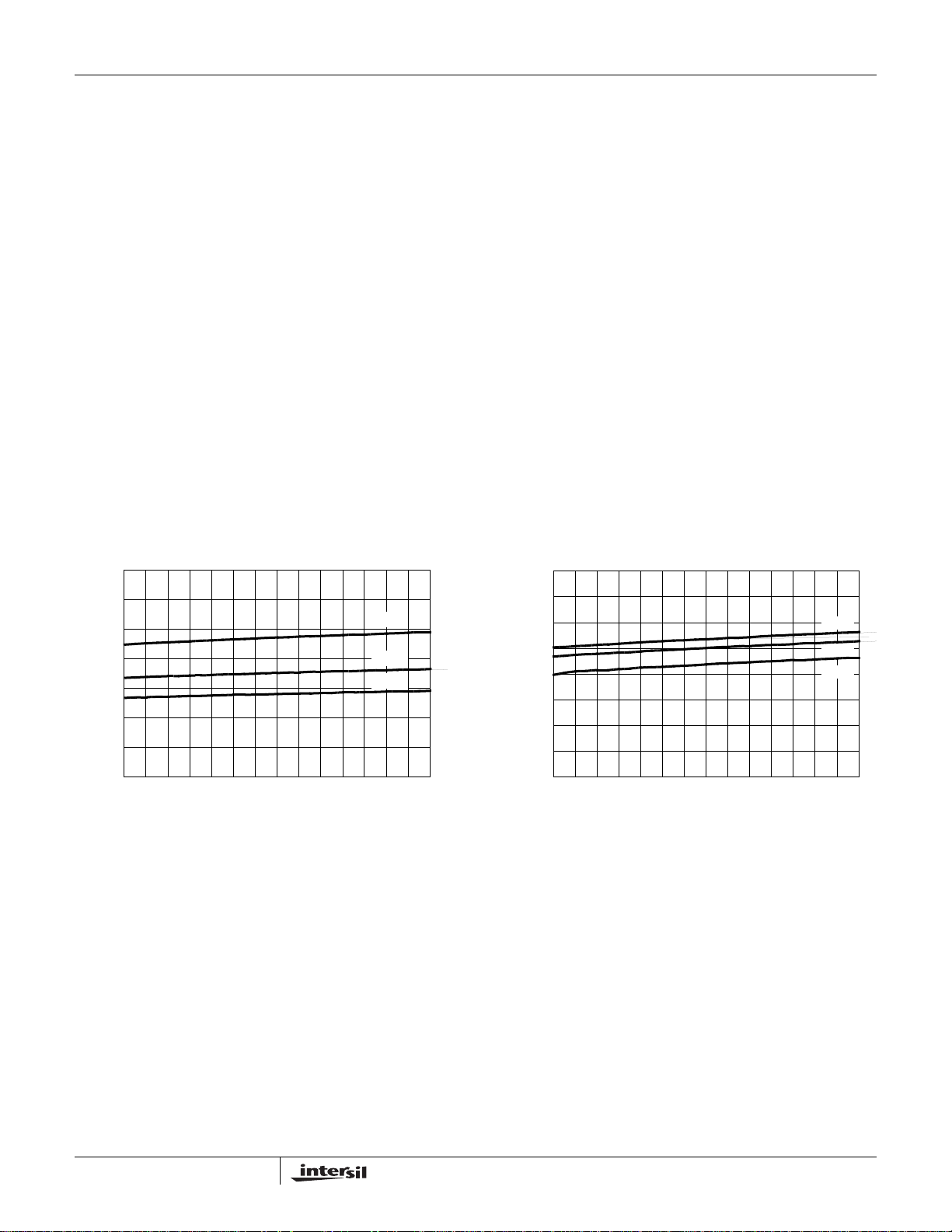
FIGURE 71. I
= 0mA, TA = 25°C unless otherwise specified
OUT
UNIT 3 (570nA)
UNIT 2 (380nA)
UNIT 1 (260nA)
2.5 3.0 3.5 4.0 4.5 5.0 5.5
(V)
V
IN
vs VIN (3 REPRESENTATIVE UNITS) FIGURE 72. IIN vs VIN OVER TEMPERATURE
IN
2.502
2.5015
2.501
UNIT 2
UNIT 1
460
440
420
400
380
(nA)
IN
I
360
340
320
300
2.5 3.0 3.5 4.0 4.5 5.0 5.5
OUT
= 2.50V
+85°C
+25°C
-40°C
V
(V)
IN
2.5005
(V)
OUT
V
(V)
OUT
V
FIGURE 73. V
2.50016
= 3V
2.50012
IN
2.50008
2.50004
2.50000
2.49996
NORMAILIZED TO 2.50V AT V
2.49992
2.5 3.0 3.5 4.0 4.5 5.0 5.5
UNIT 1
UNIT 3
V
(V)
IN
UNIT 3
2.5
2.4995
2.499
2.4985
-40 -15 10 35 60 85
TEMPERATURE (°C)
vs TEMPERATURE NORMALIZED TO 25°C
OUT
200
UNIT 2
150
= 3.0V)
100
IN
(µV)
50
O
∆V
0
-50
(NORMALIZED TO V
-100
2.5 3.0 3.5 4.0 4.5 5.0 5.5
+25°C
(V)
V
IN
-40°C
+85°C
FIGURE 74. LINE REGULATION (3 REPRESENTATIVE UNITS) FIGURE 75. LINE REGULATION OVER TEMPERATURE
21
Page 22

ISL60002
Typical Performance Characteristic Curves ISL60002, V
V
IN
= 3.0V, I
0
-10
-20
-30
-40
PSRR (dB)
-50
-60
-70
-80
= 0mA, TA = 25°C unless otherwise specified
OUT
CL = 0nF
100mV/DIV
∆V
= -0.30V
IN
1ms/DIV
∆V
= 0.30V
IN
100mV/DIV
FIGURE 76. LINE TRANSIENT RESPONSE FIGURE 77. LINE TRANSIENT RESPONSE
0.20
NO LOAD
0.10
1nF LOAD
10nF LOAD
100nF LOAD
1 10 100 1k 10k 100k 1M
FREQUENCY (Hz)
(mV)
OUT
∆V
0.00
-0.10
FIGURE 78. PSRR vs CAPACITIVE LOAD FIGURE 79. LOAD REGULATION
= 2.50V (Continued)
OUT
CL = 1nF
∆V
∆V
= -0.30V
IN
1ms/DIV
+85°C
+25°C
-40°C
-7-6-5-4-3-2-101234567
SINKING
OUTPUT CURRENT (mA)
= 0.30V
IN
SOURCING
50mV/DIV
IL = -50µA
200µs/DIV
IL = 50µA
200mV/DIV
IL = -7mA
IL = 7mA
500µs/DIV
FIGURE 80. LOAD TRANSIENT RESPONSE FIGURE 81. LOAD TRANSIENT RESPONSE
22
Page 23

ISL60002
Typical Performance Characteristic Curves ISL60002, V
V
IN
= 3.0V, I
3.5
3.0
2.5
(V)
2.0
OUT
1.5
AND V
IN
V
1.0
0.5
= 0mA, TA = 25°C unless otherwise specified
OUT
200
IIN = 380nA
0
-11357911
TIME (ms)
(Ω)
OUT
Z
150
100
50
0
FIGURE 82. TURN-ON TIME (25°C) FIGURE 83. Z
1
= 2.50V (Continued)
OUT
1nF LOAD
10 100 1k 10k 100k
FREQUENCY (Hz)
vs FREQUENCY
OUT
NO LOAD
10nF LOAD
100nF LOAD
10µV/DIV
10s/DIV
FIGURE 84. V
OUT
NOISE
23
Page 24

5
ISL60002
Typical Performance Characteristic Curves ISL60002, V
VIN = 3.0V, I
600
550
500
450
400
350
(nA)
IN
I
300
250
200
150
100
FIGURE 85. I
= 0mA, TA = 25°C unless otherwise specified
OUT
450nA
360nA
240nA
3.5 3.7 3.9 4.1 4.3 4.5 4.7 4.9 5.1 5.3 5.5
V
(V)
IN
vs VIN (3 REPRESENTATIVE UNITS) FIGURE 86. IIN vs VIN OVER TEMPERATURE
IN
3.3008
3.3006
3.3004
3.3002
(V)
OUT
3.2998
V
3.2996
3.2994
3.2992
3.299
UNIT 3
3.3
UNIT 2
-40 -15 10 35 60 85
FIGURE 87. V
UNIT 1
vs TEMPERATURE NORMALIZED TO 25°C
OUT
400
380
360
340
(nA)
IN
320
I
300
280
260
TEMPERATURE (°C)
3.5 3.7 3.9 4.1 4.3 4.5 4.7 4.9 5.1 5.3 5.5
OUT
= 3.3V
85°C
25°C
V
IN
-40°C
(V)
(V)
OUT
V
3.3002
3.30015
=5V)
IN
3.3001
450nA
3.30005
3.3
240nA
3.29995
3.2999
3.29985
3.2998
3.29975
(NORMAILIZED TO 3.30V AT V
3.2997
360nA
3.5 3.7 3.9 4.1 4.3 4.5 4.7 4.9 5.1 5.3 5.5
V
(V)
IN
150
125
100
75
= 5.0V)
50
IN
25
(µV)
0
O
-25
∆V
-50
-75
-100
(NORMALIZED TO V
-125
-150
3.5 3.7 3.9 4.1 4.3 4.5 4.7 4.9 5.1 5.3 5.
+85°C
-40°C
25°C
VIN (V)
FIGURE 88. LINE REGULATION (3 REPRESENTATIVE UNITS) FIGURE 89. LINE REGULATION OVER TEMPERATURE
24
Page 25

ISL60002
Typical Performance Characteristic Curves ISL60002, V
V
IN
= 3.0V, I
= 0mA, TA = 25°C unless otherwise specified
OUT
CL = 0nF
100mV/DIV
∆V
∆V
= -0.30V
IN
= 0.30V
IN
1ms/DIV
FIGURE 90. LINE TRANSIENT RESPONSE FIGURE 91. LINE TRANSIENT RESPONSE
0
-10
-20
-30
-40
-50
-60
PSRR (dB)
-70
-80
-90
-100
1 10 100 1k 10k 100k 1M
FREQUENCY (Hz)
FIGURE 92. PSRR vs CAPACITIVE LOAD
= 3.3V (Continued)
OUT
CL = 1nF
100mV/DIV
= -0.30V
∆V
IN
NO LOAD
1nF LOAD
10nF LOAD
100nF LOAD
1ms/DIV
∆V
= 0.30V
IN
0.60
0.50
0.40
0.30
0.20
0.10
(mV)
0.00
OUT
-0.10
V
∆
-0.20
-0.30
-0.40
-0.50
-0.60
-7 -6 -5 -4 -3 -2 -1 0 1 2 3 4 5 6 7
SINKING
FIGURE 93. LOAD REGULATION I
+85°C
25°C
-40°C
OUTPUT CURRENT (mA)
SOURCE-ISINK
25
1.00
SOURCING
0.80
0.60
0.40
0.20
(mV)
0.00
OUT
-0.20
∆V
-0.40
-0.60
-0.80
-1.00
-20-18-16-14-12-10 -8 -6 -4 -2 0 2 4 6 8 10 12 14 16 18 20
25°C
-40°C
SINKING
+85°C
OUTPUT CURRENT (mA)
= ±7mA FIGURE 94. LOAD REGULATION I
SOURCE-ISINK
SOURCING
= ±20mA
Page 26

ISL60002
Typical Performance Characteristic Curves ISL60002, V
V
IN
= 3.0V, I
= 0mA, TA = 25°C unless otherwise specified
OUT
200mV/DIV
IL = -50µA
IL = 50µA IL = -1mA
200µs/DIV
FIGURE 95. LOAD TRANSIENT RESPONSE FIGURE 96. LOAD TRANSIENT RESPONSE
= 3.3V (Continued)
OUT
1V/DIV
IL = 1mA
200µs/DIV
1V/DIV
IL = -7mA
IL = 7mA IL = -20mA
200µs/DIV
1V/DIV
200µs/DIV
FIGURE 97. LOAD TRANSIENT RESPONSE FIGURE 98. LOAD TRANSIENT RESPONSE
160
5
4
(V)
3
OUT
and V
2
IN
V
1
0
024681012
TIME (ms)
V
360nA
IN
FIGURE 99. TURN-ON TIME (25°C) FIGURE 100. Z
140
120
100
(Ω)
80
OUT
Z
60
40
20
0
1 10 100 1k 10k 100k
FREQUENCY (Hz)
vs FREQUENCY
OUT
IL = 20mA
NO LOAD
1nF LOAD
10nF LOAD
100nF LOAD
26
Page 27

ISL60002
Applications Information
FGA Technology
The ISL60002 series of voltage references use the floating
gate technology to create references with very low drift and
supply current. Essentially the charge stored on a floating
gate cell is set precisely in manufacturing. The reference
voltage output itself is a buffered version of the floating gate
voltage. The resulting reference device has excellent
characteristics which are unique in the industry: very low
temperature drift, high initial accuracy, and almost zero
supply current. Also, the reference voltage itself is not limited
by voltage bandgaps or zener settings, so a wide range of
reference voltages can be programmed (standard voltage
settings are provided, but customer-specific voltages are
available).
The process used for these reference devices is a floating
gate CMOS process, and the amplifier circuitry uses CMOS
transistors for amplifier and output transistor circuitry. While
providing excellent accuracy, there are limitations in output
noise level and load regulation due to the MOS device
characteristics. These limitations are addressed with circuit
techniques discussed in other sections.
Nanopower Operation
Reference devices achieve their highest accuracy when
powered up continuously, and after initial stabilization has
taken place. This drift can be eliminated by leaving the
power on continuously.
The ISL60002 is the first high precision voltage reference
with ultra low power consumption that makes it possible to
leave power on continuously in battery operated circuits. The
ISL60002 consumes extremely low supply current due to the
proprietary FGA technology. Supply current at room
temperature is typically 350nA which is 1 to 2 orders of
magnitude lower than competitive devices. Application
circuits using battery power will benefit greatly from having
an accurate, stable reference which essentially presents no
load to the battery.
In particular, battery powered data converter circuits that
would normally require the entire circuit to be disabled when
not in use can remain powered up between conversions as
shown in Figure 101. Data acquisition circuits providing 12 to
24 bits of accuracy can operate with the reference device
continuously biased with no power penalty, providing the
highest accuracy and lowest possible long term drift.
Other reference devices consuming higher supply currents
will need to be disabled in between conversions to conserve
battery capacity. Absolute accuracy will suffer as the device
is biased and requires time to settle to its final value, or, may
not actually settle to a final value as power on time may be
short.
VIN = +3.0V
V
ISL60002
GND
IN
V
OUT
0.001µF–0.01µF
10µF
SERIAL
BUS
FIGURE 101.
0.01µF
REF IN
ENABLE
SCK
SDAT
12 to 24-BIT
A/D CONVERTER
Board Mounting Considerations
For applications requiring the highest accuracy, board
mounting location should be reviewed. Placing the device in
areas subject to slight twisting can cause degradation of the
accuracy of the reference voltage due to die stresses. It is
normally best to place the device near the edge of a board,
or the shortest side, as the axis of bending is most limited at
that location. Obviously mounting the device on flexprint or
extremely thin PC material will likewise cause loss of
reference accuracy.
Noise Performance and Reduction
The output noise voltage in a 0.1Hz to 10Hz bandwidth is
typically 30µV
Performance Curves. The noise measurement is made with
a bandpass filter made of a 1 pole high-pass filter with a
corner frequency at 0.1Hz and a 2-pole low-pass filter with a
corner frequency at 12.6Hz to create a filter with a 9.9Hz
bandwidth. Noise in the 10kHz to 1MHz bandwidth is
approximately 400µV
as shown in Figure 102. These noise measurements are
made with a 2 decade bandpass filter made of a 1 pole highpass filter with a corner frequency at 1/10 of the center
frequency and 1-pole low-pass filter with a corner frequency
at 10 times the center frequency. Figure 102 also shows the
noise in the 10kHz to 1MHz band can be reduced to about
50µV
using a 0.001µF capacitor on the output. Noise in
P-P
the 1kHz to 100kHz band can be further reduced using a
0.1µF capacitor on the output, but noise in the 1Hz to 100Hz
band increases due to instability of the very low power
amplifier with a 0.1µF capacitance load. For load
capacitances above 0.001µF the noise reduction network
shown in Figure 103 is recommended. This network reduces
noise significantly over the full bandwidth. As shown in
Figure 102, noise is reduced to less than 40µV
to 1MHz using this network with a 0.01µF capacitor and a
2kΩ resistor in series with a 10µF capacitor.
. This is shown in the plot in the Typical
P-P
with no capacitance on the output,
P-P
P-P
from 1Hz
27
Page 28

ISL60002
400
350
)
300
P-P
250
200
150
100
NOISE VOLTAGE (µV
50
0
1 10 10 0 1,000 10,000 100,000
CL = 0
CL = 0.001µF
CL = 0.1µF
CL = 0.01µF & 10µF + 2kΩ
FIGURE 102. NOISE REDUCTION
VIN = 3.0V
10µF
0.1µF
V
IN
ISL60002
GND
V
O
0.01µF
FIGURE 103.
2kΩ
10µF
3.5
3.0
2.5
(V)
2.0
OUT
1.5
AND V
IN
V
1.0
0.5
0
-11357911
3.5
3.0
2.5
(V)
2.0
OUT
1.5
AND V
IN
V
1.0
0.5
580nA
580nA
V
IN
380nA
V
280nA
TIME (ms)
IN
280nA
380nA
Turn-On Time
The ISL60002 devices have ultra-low supply current and
thus the time to bias up internal circuitry to final values will
be longer than with higher power references. Normal turn-on
time is typically 7ms. This is shown in Figure 104. Since
devices can vary in supply current down to >300nA, turn-on
time can last up to about 12ms. Care should be taken in
system design to include this delay before measurements or
conversions are started.
0
-11357911
TIME (ms)
FIGURE 104. TURN-ON TIME
Temperature Coefficient
The limits stated for temperature coefficient (tempco) are
governed by the method of measurement. The
overwhelming standard for specifying the temperature drift of
a reference is to measure the reference voltage at two
temperatures, take the total variation, (V
divide by the temperature extremes of measurement
(T
HIGH–TLOW
). The result is divided by the nominal
reference voltage (at T = 25°C) and multiplied by 10
ppm/°C. This is the “Box” method for specifying temperature
coefficient.
HIGH
– V
LOW
6
to yield
), and
28
Page 29

Typical Application Circuits
VIN = 5.0V
ISL60002
R = 200Ω
V
IN
2N2905
2.7 - 5.5V
2-WIRE BUS
ISL60002
V
= 2.50V
OUT
GND
V
OUT
2.5V/50mA
0.001µF
FIGURE 105. PRECISION 2.5V 50mA REFERENCE
0.001µF
+
–
10µF
V
OUT
V
IN
ISL60002,
V
= 2.50V
OUT
GND
V
SDA
SCL
V
V
OUT
CC
X9119
SS
0.1µF
R
H
R
L
V
OUT
(BUFFERED)
FIGURE 106. 2.5V FULL SCALE LOW-DRIFT 10-BIT ADJUSTABLE VOLTAGE SOURCE
+2.7-5.5V
V
IN
ISL60002
GND
V
0.1µF
OUT
10µF
+
–
V
OUT
SENSE
LOAD
FIGURE 107. KELVIN SENSED LOAD
29
Page 30

Packaging Information
0.046 (1.18) BSC
0.055 (1.40)
0.047 (1.20)
4X
0.35 HA-BD
ISL60002
3-Lead, SOT-23, Package Code H3
0.093 (2.35) BSC
0.007 (0.20)
B
0.0003 (0.08)
C
L
B
0.35 CA-BD
2X N/2 TIPS
0.034 (0.88)
0.047 (1.02)
0.0004 (0.01)
0.0040 (0.10)
0.035 (0.89)
0.044 (1.12)
1
0.075 (1.90) BSC
0.120 (3.04)
0.110 (2.80)
0.038 (0.95)
BSC
2
Parting Line
Seating Plane
0.10 R MIN.
0.20 in
0–8°C
12° REF.
TYP.
0.575 REF.
0.10 R MIN.
SEATING PLANE
.024 (0.60)
.016 (0.40)
NOTES:
1. All dimensions in inches (in parentheses in millimeters).
2. Package dimensions exclude molding flash.
3. Die and die paddle is facing down towards seating plane.
4. This part is compliant with JEDEC Specification TO-236AB.
5. Dimensioning and tolerances per ASME, Y14.5M-1994.
30
Page 31

Packaging Information
ISL60002
8-Lead Plastic, SOIC, Package Code B8
0° - 8°
Pin 1 Index
0.010 (0.25)
0.020 (0.50)
0.016 (0.410)
0.037 (0.937)
Pin 1
(4X) 7°
0.050 (1.27)
X 45°
0.014 (0.35)
0.019 (0.49)
0.188 (4.78)
0.197 (5.00)
0.0075 (0.19)
0.010 (0.25)
0.150 (3.80)
0.158 (4.00)
0.004 (0.19)
0.010 (0.25)
0.250"
FOOTPRINT
0.228 (5.80)
0.244 (6.20)
0.053 (1.35)
0.069 (1.75)
0.050" Typical
0.050"
Typical
0.030"
Typical
8 Places
NOTE: All dimensions in inches (in parentheses in millimeters).
All Intersil U.S. products are manufactured, assembled and tested utilizing ISO9000 quality systems.
Intersil Corporation’s quality certifications can be viewed at www.intersil.com/design/quality
Intersil products are sold by description only. Intersil Corporation reserves the right to make changes in circuit design, software and/or specifications at any time without
notice. Accordingly, the reader is cautioned to verify that data sheets are current before placing orders. Information furnished by Intersil is believed to be accurate and
reliable. However, no responsibility is assumed by Intersil or its subsidiaries for its use; nor for any infringements of patents or other rights of third parties which may result
from its use. No license is granted by implication or otherwise under any patent or patent rights of Intersil or its subsidiaries.
For information regarding Intersil Corporation and its products, see www.intersil.com
31
 Loading...