

Page 1
®
ISL59446
Data Sheet May 19, 2006
500MHz Triple 4:1 Gain-of-2, Multiplexing
Amplifier
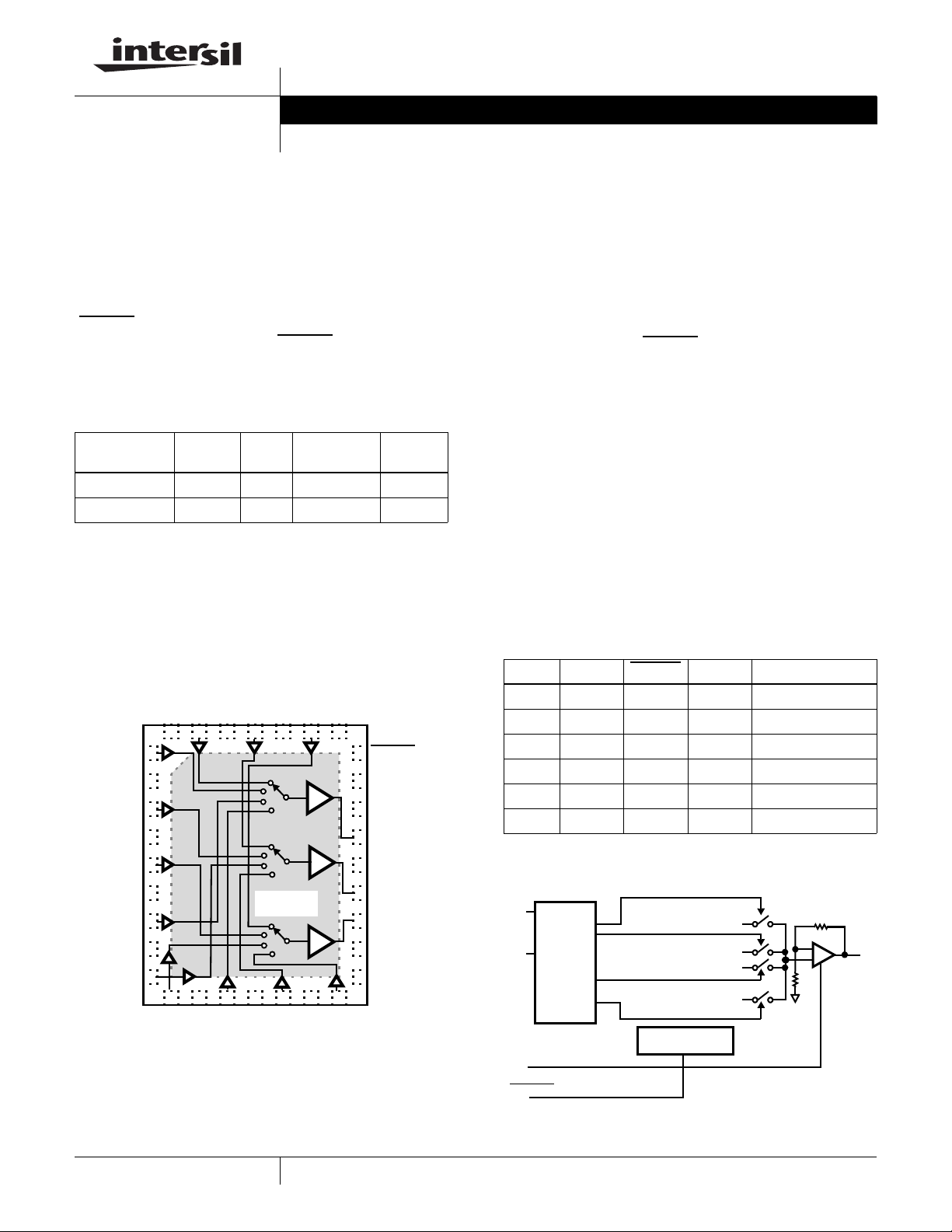
The ISL59446 is a triple channel 4:1 multiplexer featuring
integrated amplifiers with a fixed gain of 2, high slew-rate
and excellent bandwidth for video switching. The device
features a three-state output (HIZ), which allows the outputs
of multiple devices to be tied together. A power-down mode
(EN
ABLE) is included to turn off un-needed circuitry in power
sensitive applications. When the EN
ABLE pin is pulled high,
the part enters a power-down mode and consumes just
14mW.
Ordering Information
PART NUMBER
(Note)
ISL59446IRZ IRZ - 32 Ld QFN L32.5x6A
ISL59446IRZ-T7 IRZ 7” 32 Ld QFN L32.5x6A
NOTE: Intersil Pb-free plus anneal products employ special Pb-free
material sets; molding compounds/die attach materials and 100%
matte tin plate termination finish, which are RoHS compliant and
compatible with both SnPb and Pb-free soldering operations. Intersil
Pb-free products are MSL classified at Pb-free peak reflow
temperatures that meet or exceed the Pb-free requirements of
IPC/JEDEC J STD-020.
PART
MARKING
TAPE &
REEL
PACKAGE
(Pb-Free)
PKG.
DWG. #
Pinout
GNDA
IN0A
NIC
IN0B
NIC
IN0C
HIZ
32
31
30
29
28
x2
x2
x2
15 27
NIC
16 26
IN3C
25
24
23
22
21
20
19
18
17
ENABLE
NIC
V+
OUTA
V-
OUTB
OUTC
S0
S1
1
IN1A
2
NIC
3
IN1B
4
NIC
5
IN1C
6
GNDB
7
IN2A
8
NIC
IN2B
9
10
11
IN2C
GNDC
THERMAL PAD INTERNALLY CONNECTED TO V-. PAD MUST BE
TIED TO V-
NIC = NO INTERNAL CONNECTION
12
IN3A
THERMAL
PAD
13
14
NIC
IN3B
FN6261.0
Features
• 510MHz bandwidth into 150Ω
• ±1600V/µs slew rate
• High impedance buffered inputs
• Internally set gain-of-2
• High speed three-state outputs (HIZ)
• Power-down mode (EN
ABLE)
• ±5V operation
• Supply current 11mA/ch
• Pb-free plus anneal available (RoHS compliant)
Applications
• HDTV/DTV analog inputs
• Video projectors
• Computer monitors
• Set-top boxes
• Security video
• Broadcast video equipment
TABLE 1. CHANNEL SELECT LOGIC TABLE ISL59446
S1 S0 ENABLE
0 0 0 0 IN0 (A, B, C)
0 1 0 0 IN1 (A, B, C)
1 0 0 0 IN2 (A, B, C)
1 1 0 0 IN3 (A, B, C)
X X 1 X Power-Down
XX 0 1 High Z
HIZ OUTPUT
Functional Diagram (each channel)
EN0
S0
S1
HIZ
ENABLE
DECODE
IN0(A, B, C)
EN1
IN1(A, B, C)
IN2(A, B, C)
EN2
IN3(A, B, C)
EN3
AMPLIFIER BIAS
+
OUT
1
CAUTION: These devices are sensitive to electrostatic discharge; follow proper IC Handling Procedures.
1-888-INTERSIL or 1-888-468-3774
| Intersil (and design) is a registered trademark of Intersil Americas Inc.
All other trademarks mentioned are the property of their respective owners.
Copyright © Intersil Americas Inc. 2006. All Rights Reserved.
Page 2
ISL59446
Absolute Maximum Ratings (T
Supply Voltage (V+ to V-). . . . . . . . . . . . . . . . . . . . . . . . . . . . . . .11V
Input Voltage . . . . . . . . . . . . . . . . . . . . . . . . . . . . V- -0.5V, V+ +0.5V
Supply Turn-on Slew Rate . . . . . . . . . . . . . . . . . . . . . . . . . . . 1V/µs
Digital & Analog Input Current (Note 1) . . . . . . . . . . . . . . . . . . 50mA
= 25°C)
A
Storage Temperature Range. . . . . . . . . . . . . . . . . .-65°C to +150°C
Ambient Operating Temperature . . . . . . . . . . . . . . . .-40°C to +85°C
Operating Junction Temperature. . . . . . . . . . . . . . .-40°C to +125°C
Power Dissipation . . . . . . . . . . . . . . . . . . . . . . . . . . . . . .See Curves
Output Current (Continuous) . . . . . . . . . . . . . . . . . . . . . . . . . . 50mA
ESD Rating
Human Body M odel (Per MIL -STD-883 Met h od 3015.7). . . .2500V
Machine Model . . . . . . . . . . . . . . . . . . . . . . . . . . . . . . . . . . .300V
CAUTION: Stresses above those listed in “Absolute Maximum Ratings” may cause permanent damage to the device. This is a stress only rating and operation of the
device at these or any other conditions above those indicated in the operational sections of this specification is not implied.
NOTE:
1. If an input signal is applied before the supplies are powered up, the input current must be limited to these maximum values.
IMPORTANT NOTE: All parameters having Min/Max specifications are guaranteed. Typical values are for information purposes only. Unless otherwise noted, all tests
are at the specified temperature and are pulsed tests, therefore: T
Electrical Specifications V+ = +5V , V- = -5V, GND = 0V, T
specified.
= TC = T
J
A
= 25°C, V
A
OUT
= ±2V
and RL = 500Ω to GND, CL = 0pF, unless otherwise
P-P
PARAMETER DESCRIPTION CONDITIONS MIN TYP MAX UNIT
GENERAL
+I
Enabled Enabled Supply Current No load, VIN = 0V, Enable Low 40 44 48 mA
S
-I
Enabled Enabled Supply Current No load, VIN = 0V, Enable Low -45 -41 -37 mA
S
+I
Disabled Disabled Supply Current No load, VIN = 0V, Enable High 3 3.4 3.8 mA
S
-IS Disabled Disabled Supply Current No load, VIN = 0V, Enable High -40 -6 µA
V
OUT
I
OUT
V
OS
Ib Input Bias Current V
R
OUT
R
OUT
R
IN
or A
A
CL
Positive and Negative Output Swing V
= ±2.5V; RL = 500Ω ±3.8 ±4.0 ±4.2 V
IN
Output Current VIN = 0.825V RL = 10Ω ±80 ±135 ±180 mA
Output Offset Voltage -40 -25 -10 mV
= 0V -4 -2 -1 µA
IN
HIZ Output Resistance HIZ = Logic High 700 900 1150 Ω
Enabled Output Resistance HIZ = Logic Low 0.2 Ω
Input Resistance VIN = ±1.75V 10 MΩ
Voltage Gain RL = 500Ω 1.94 1.99 2.04 V/V
V
LOGIC
V
IH
V
IL
I
IH
I
IL
Input High Voltage (Logic Inputs) 2 V
Input Low Voltage (Logic Inputs) 0.8 V
Input High Current (Logic Inputs) VH = 5V 200 260 320 µA
Input Low Current (Logic Inputs) VL = 0V -4 -2 -1 µA
AC GENERAL
PSRR Power Supply Rejection Ratio DC, PSRR V+ and V- combined
V
= 0dBm
OUT
Xtalk Channel to Channel Crosstalk f = 10MHz, ChX-Ch Y-Talk
V
= 1V
IN
; CL = 1.1pF
P-P
Off - ISO Off-State Isolation f = 10MHz, Ch-Ch Off Isolation
= 1V
V
IN
dG Differential Gain Error NTC-7, R
dP Differential Phase Error NTC-7, R
; CL = 1.1pF
P-P
= 150, CL = 1.1pF 0.008 %
L
= 150, CL = 1.1pF 0.01 °
L
45 53 dB
74 dB
76 dB
2
FN6261.0
May 19, 2006
Page 3

ISL59446
Electrical Specifications V+ = +5V, V- = -5V, GND = 0V, T
specified. (Continued)
= 25°C, V
A
OUT
= ±2V
and RL = 500Ω to GND, CL = 0pF , unless otherwise
P-P
PARAMETER DESCRIPTION CONDITIONS MIN TYP MAX UNIT
BW Small Signal -3dB Bandwidth V
Large Signal -3dB Bandwidth V
FBW 0.1dB Bandwidth V
SR Slew Rate 25% to 75%, R
V
V
V
C
OUT
OUT
OUT
OUT
OUT
OUT
L
= 0.2V
= 0.2V
= 2V
= 2V
= 2V
= 2V
= 2.1pF
; RL = 500Ω, CL = 1.1pF 620 MHz
P-P
; RL = 150Ω, CL = 2.1pF 530 MHz
P-P
; RL = 500Ω, CL = 1.1pF 280 MHz
P-P
; RL = 150Ω, CL = 1.1pF 260 MHz
P-P
; RL = 500Ω, CL = 1.1pF 160 MHz
P-P
; RL = 150Ω, CL = 1.1pF 50 MHz
P-P
= 150Ω, Input Enabled,
L
1600 V/µs
TRANSIENT RESPONSE
tr, tf Large
Signal
tr, tf, Small
Signal
ts 0.1%
ts 1%
Large Signal Rise, Fall Times, tr, tf,
10% - 90%
Small Signal Rise, Fall Times, tr, tf,
10% - 90%
Settling TIme to 0.1% V
Settling TIme to 1% V
V
V
V
V
V
V
OUT
OUT
OUT
OUT
OUT
OUT
OUT
OUT
= 2V
= 2V
= 0.2V
= 0.2V
= 2V
= 2V
= 2V
= 2V
; RL = 500Ω, CL = 1.1pF 1.2 ns
P-P
; RL = 150Ω, CL = 2.1pF 1.3 ns
P-P
; RL = 500Ω, CL = 1.1pF 0.7 ns
P-P
; RL = 150Ω, CL = 2.1pF 0.9 ns
P-P
; RL = 500Ω, CL = 1.1pF 7.2 ns
P-P
; RL = 150Ω, CL = 2.1pF 8.2 ns
P-P
; RL = 500Ω, CL = 1.1pF 4 ns
P-P
; RL = 150Ω, CL = 2.1pF 4.3 ns
P-P
SWITCHING CHARACTERISTICS
V
GLITCH
Channel -to-Channel Switching Glitch VIN = 0V, RL = 500Ω; CL = 1.1pF 90 mV
VIN = 0V, RL = 150Ω; CL = 2.1pF 15 mV
Enable Switching Glitch VIN = 0V, RL = 500Ω; CL = 1.1pF 1.8 V
VIN = 0V, RL = 150Ω; CL = 2.1pF 1.35 V
HIZ Switching Glitch VIN = 0V, RL = 500Ω; CL = 1.1pF 340 mV
VIN = 0V, RL = 150Ω; CL = 2.1pF 340 mV
t
SW-L-H
Channel Switching Time Low to High 1.2V logic threshold to 10% movement of
24 ns
analog output
t
SW-H-L
Channel Switching Time High to Low 1.2V logic threshold to 10% movement of
analog output
24 ns
tpd Propagation Delay 10% to 10% 0.55 ns
P-P
P-P
P-P
P-P
P-P
P-P
3
FN6261.0
May 19, 2006
Page 4
ISL59446
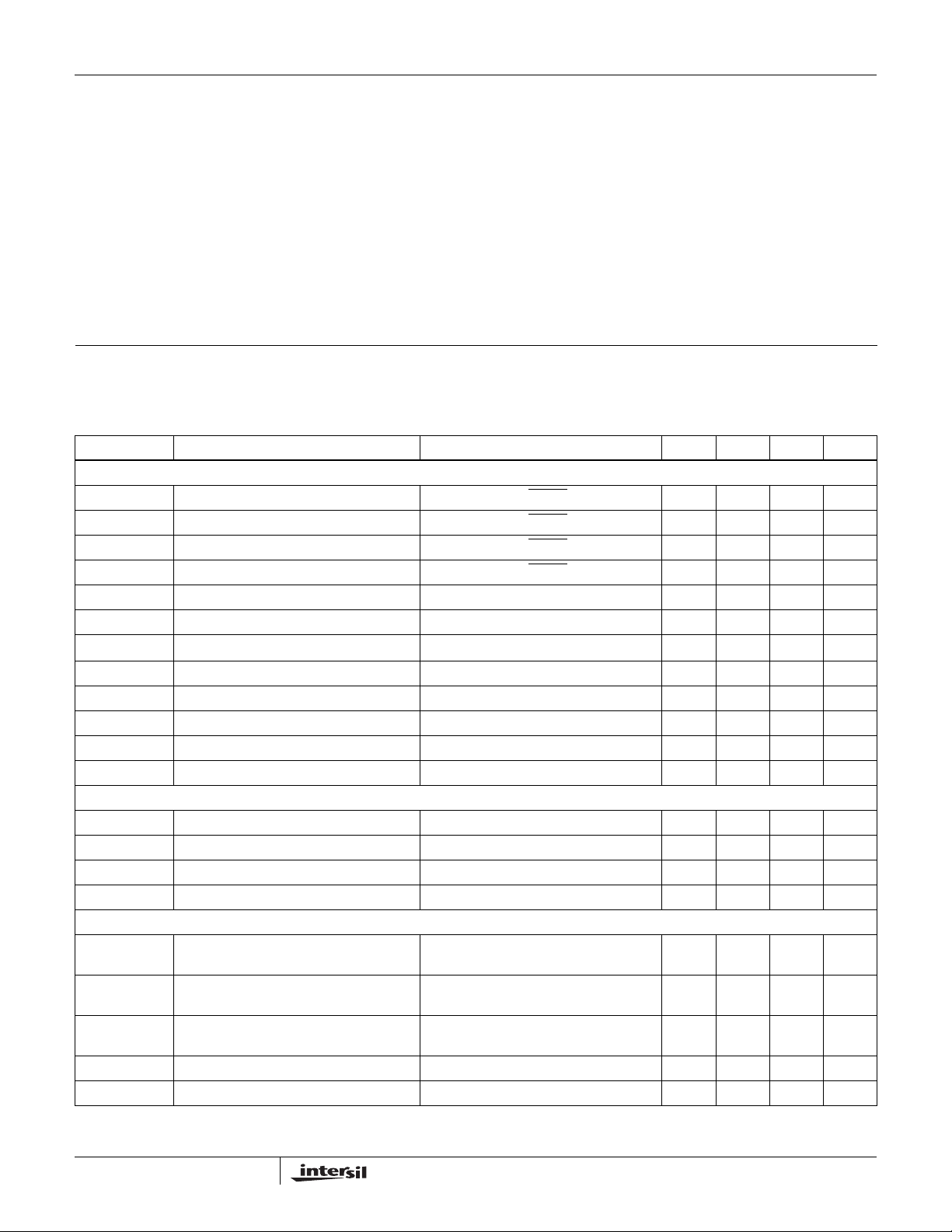
Typical Performance Curves V
10
V
= 0.2V
OUT
8
6
4
2
0
-2
-4
NORMALIZED GAIN (dB)
-6
CL INCLUDES 0.6pF
-8
BOARD CAPACITANCE
-10
1M 10M 100M 1G
P-P
FREQUENCY (Hz)
CL = 8.8pF
CL = 7.4pF
CL = 6.2pF
CL = 4.5pF
CL = 3.3pF
CL = 2.1pF
CL = 1.1pF
= ±5V, RL = 500Ω to GND, TA = 25°C, unless otherwise specified.
S
CL = 0.6pF
FIGURE 1. SMALL SIGNAL GAIN vs FREQUENCY vs C
INTO 500Ω LOAD
10
V
= 2V
OUT
8
6
4
2
0
-2
-4
NORMALIZED GAIN (dB)
-6
CL INCLUDES 0.6pF
-8
BOARD CAPACITANCE
-10
1M 10M 100M 1G
P-P
FREQUENCY (Hz)
CL = 8.8pF
CL = 5.3pF
CL = 2.1pF
CL = 0.6pF
FIGURE 3. LARGE SIGNAL GAIN vs FREQUENCY vs C
INTO 500Ω LOAD
10
V
= 0.2V
OUT
8
6
4
2
0
-2
-4
NORMALIZED GAIN (dB)
-6
CL INCLUDES 0.6pF
-8
BOARD CAPACITANCE
-10
1M 10M 100M 1G
L
L
FIGURE 2. SMALL SIGNAL GAIN vs FREQUENCY vs CL
10
V
OUT
8
6
4
2
0
-2
-4
NORMALIZED GAIN (dB)
-6
CL INCLUDES 0.6pF
-8
BOARD CAPACITANCE
-10
1M 10M 100M 1G
FIGURE 4. LARGE SIGNAL GAIN vs FREQUENCY vs C
P-P
FREQUENCY (Hz)
INTO 150Ω LOAD
= 2V
P-P
FREQUENCY (Hz)
INTO 150Ω LOAD
CL = 12.6pF
CL = 10.6pF
CL = 8.8pF
CL = 6.2pF
CL = 4.5pF
CL = 3.3pF
CL = 2.1pF
CL = 12.6pF
CL = 5.3pF
CL = 2.1pF
CL = 0.6pF
CL = 0.6pF
L
2
V
= 0.2V
OUT
CL = 1.1pF
1
0
-1
-2
-3
-4
-5
NORMALIZED GAIN (dB)
-6
-7
-8
1M 10M 100M 1G
P-P
RL = 250Ω
RL = 150Ω
FREQUENCY (Hz)
RL = 1kΩ
RL = 500Ω
FIGURE 5. GAIN vs FREQUENCY vs R
4
0.3
V
= 0.2V
OUT
0.2
0.1
0
-0.1
-0.2
-0.3
-0.4
NORMALIZED GAIN (dB)
-0.5
-0.6
-0.7
1M 10M 100M 1G
L
P-P
RL = 500Ω
CL = 1.1pF
FREQUENCY (Hz)
FIGURE 6. 0.1dB GAIN FLATNESS
RL = 150Ω
= 2.1pF
C
L
FN6261.0
May 19, 2006
Page 5

ISL59446
Typical Performance Curves V
100
V
10
1
OUTPUT IMPEDANCE (Ω)
0.1
0.1M 1M 10M 100M 1G
FIGURE 7. Z
1M
100k
10k
1k
100
INPUT IMPEDANCE (Ω)
10
SOURCE
= 2V
P-P
FREQUENCY (Hz)
vs FREQUENCY - ENABLED
OUT
V
SOURCE
= ±5V, RL = 500Ω to GND, TA = 25°C, unless otherwise specified. (Continued)
S
10k
= 2V
P-P
V
1k
100
OUTPUT IMPEDANCE (Ω)
10
0.1M 1M 10M 100M 1G
10
0
-10
-20
-30
PSRR (dB)
-40
-50
= 2V
SOURCE
FIGURE 8. Z
V
SOURCE
PSRR (V-)
= 0.5V
P-P
FREQUENCY (Hz)
vs FREQUENCY - HIZ
OUT
P-P
PSRR (V-)
1
0.3M 1M 10M 100M 1G
FIGURE 9. Z
0
VIN = 1V
-10
-20
-30
INPUT X TO OUTPUT Y R
-40
INPUT X TO OUTPUT X R
-50
(dB)
-60
-70
-80
-90
-100
0.1M 1M 10M 100M 1G
P-P
CROSSTALK RL = 500
OFF ISOLATION RL = 500
FREQUENCY (Hz)
vs FREQUENCY
IN
= 150
L
= 150
L
FREQUENCY (Hz)
FIGURE 11. CROSSTALK AND OFF ISOLATION
5
-60
0.3M 1M 10M 100M 1G
FREQUENCY (Hz)
FIGURE 10. PSRR vs FREQUENCY
60
50
40
30
20
VOLTAGE NOISE (nV/√Hz)
10
0
100 1k 10k 100k
FREQUENCY (Hz)
FIGURE 12. INPUT NOISE vs FREQUENCY
FN6261.0
May 19, 2006
Page 6

ISL59446
Typical Performance Curves V
0.002
0
-0.002
-0.004
-0.006
-0.008
-0.01
NORMALIZED GAIN (dB)
0.02
0
-0.02
-0.04
-0.06
-0.08
-0.10
NORMALIZED PHASE (°)
V
OUT
FIGURE 13. DIFFERENTIAL GAIN AND PHASE;
V
0.2
OUT
=0.2V
, FO = 3.58MHz, RL = 500Ω
P-P
0
DC (V)
1234-4 -3 -2 -1
= ±5V, RL = 500Ω to GND, TA = 25°C, unless otherwise specified. (Continued)
S
0.01
0.008
0.006
0.004
0.002
0
-0.002
-0.004
NORMALIZED GAIN (dB)NORMALIZED PHASE (°)
0.04
0.02
0
-0.02
-0.04
-0.06
-0.08
-0.10
V
OUT
0
DC (V)
1234-4 -3 -2 -1
FIGURE 14. DIFFERENTIAL GAIN AND PHASE;
V
= 0.2V
OUT
RL = 500Ω
CL = 1.1pF
P-P
0.2
V
OUT
=0.2V
, FO = 3.58MHz, RL = 150Ω
P-P
V
= 0.2V
OUT
RL = 150Ω
CL = 2.1pF
P-P
0.1
OUTPUT VOLTAGE (V)
0
TIME (5ns/DIV)
FIGURE 15. SMALL SIGNAL TRANSIENT RESPONSE;
R
=500Ω
L
= 2V
V
OUT
RL = 500Ω
2.0
1.0
OUTPUT VOLTAGE (V)
0
CL = 1.1pF
P-P
0.1
OUTPUT VOLTAGE (V)
0
TIME (5ns/DIV)
FIGURE 16. SMALL SIGNAL TRANSIENT RESPONSE;
RL= 150Ω
= 2V
V
OUT
RL = 150Ω
2.0
1.0
OUTPUT VOLTAGE (V)
0
CL = 2.1pF
P-P
TIME (5ns/DIV)
FIGURE 17. LARGE SIGNAL TRANSIENT RESPONSE;
R
=500Ω
L
6
TIME (5ns/DIV)
FIGURE 18. LARGE SIGNAL TRANSIENT RESPONSE;
RL= 150Ω
May 19, 2006
FN6261.0
Page 7

ISL59446
Typical Performance Curves V
50
INPUT RISE, FALL TIMES
<175ps
V
= 1.4V
40
30
20
OVERSHOOT (%)
10
0
OUT
2
FIGURE 19. PULSE OVERSHOOT vs V
S0, S1
50Ω
TERM.
4
V
P-P
CL (pF)
OUT
= 2V
V
V
OUT
6
OUT
OUT
= ±5V, RL = 500Ω to GND, TA = 25°C, unless otherwise specified. (Continued)
S
50
P-P
= 1V
P-P
= 0.2V
P-P
8
10
, CL; RL = 500Ω FIGURE 20. PULSE OVERSHOOT vs V
VIN = 0V
INPUT RISE, FALL TIMES
<175ps
40
V
= 1.4V
OUT
30
20
OVERSHOOT (%)
10
0
S0, S1
50Ω
TERM.
V
= 2V
OUT
P-P
P-P
V
V
OUT
2
4
CL (pF)
6
OUT
= 1V
OUT
P-P
= 0.2V
P-P
8
, CL; RL = 150Ω
VIN = 1V
10
1V/DIV20mV/DIV
0
V
A, B, C
OUT
0
20ns/DIV
FIGURE 21. CHANNEL TO CHANNEL SWITCHING GLITCH
V
=0V
IN
1V/DIV1V/DIV
0
0
ENABLE
50Ω
TERM.
V
OUT
A, B, C
VIN = 0V
1V/DIV1V/DIV
0
0
V
A, B, C
OUT
20ns/DIV
FIGURE 22. CHANNEL TO CHANNEL TRANSIENT RESPONSE
VIN=1V
VIN = 1V
1V/DIV2V/DIV
ENABLE
50Ω
TERM.
0
0
V
OUT
A, B, C
FIGURE 23. ENABLE
40ns/DIV
40ns/DIV
SWITCHING GLITCH VIN = 0V FIGURE 24. ENABLE TRANSIENT RESPONSE V
7
= 1V
IN
FN6261.0
May 19, 2006
Page 8

ISL59446
Typical Performance Curves V
HIZ
50Ω
TERM.
1V/DIV200mv/DIV
0
0
V
A, B, C
OUT
20ns/DIV
FIGURE 25. HIZ SWITCHING GLITCH VIN = 0V FIGURE 26. HIZ TRANSIENT RESPONSE V
JEDEC JESD51-7 HIGH EFFECTIVE THERMAL
CONDUCTIVITY TEST BOARD - QFN EXPOSED
DIEPAD SOLDERED TO PCB PER JESD51-5
3
2.857W
2.5
2
1.5
QFN32
θJA = 35°C/W
= ±5V, RL = 500Ω to GND, TA = 25°C, unless otherwise specified. (Continued)
S
1V/DIV
2V/DIV
HIZ
50Ω
TERM.
0
V
A, B, C
OUT
0
20ns/DIV
JEDEC JESD51-3 LOW EFFECTIVE THERMAL
CONDUCTIVITY TEST BOARD
1.2
1
0.8
758mW
0.6
VIN = 0V
VIN = 1V
= 1V
IN
1
POWER DISSIPATION (W)
0.5
0
0 25 50 75 100 150
AMBIENT TEMPERATURE (°C)
12585
FIGURE 27. PACKAGE POWER DISSIP A TION vs AMBIENT
TEMPERATURE
0.4
POWER DISSIPATION (W)
0.2
0
0 25 50 75 100 150
QFN32
θ
= 125°C/W
JA
AMBIENT TEMPERATURE (°C)
12585
FIGURE 28. PACKAGE POWER DISSIP A TION vs AMBIENT
TEMPERATURE
8
FN6261.0
May 19, 2006
Page 9
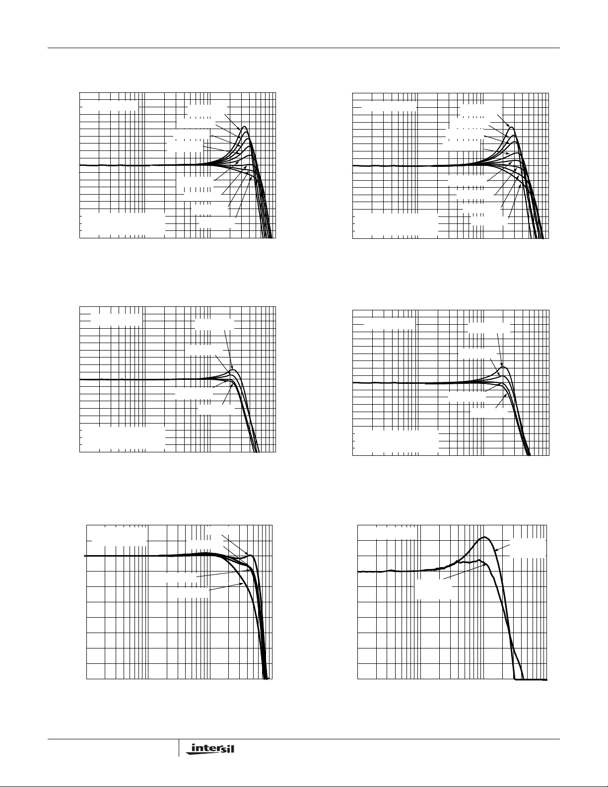
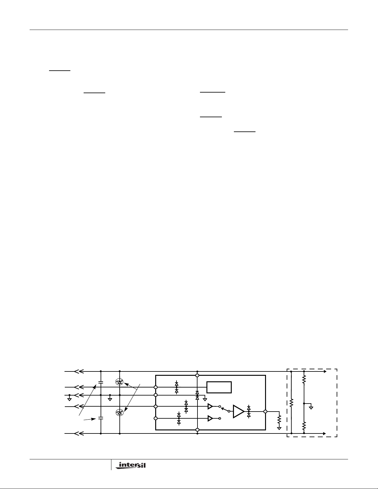
Pin Descriptions
ISL59446
ISL59446
(32 LD QFN) PIN NAME
EQUIVALENT
CIRCUIT DESCRIPTION
1 IN1A Circuit 1 Channel 1 input for output amplifier "A"
2, 4, 8, 13, 15, 24,
28, 30
NIC Not Internally Connected; it is recommended these pins be tied to ground to minimize
crosstalk.
3 IN1B Circuit 1 Channel 1 input for output amplifier "B"
5 IN1C Circuit 1 Channel 1 input for output amplifier "C"
6 GNDB Circuit 4 Ground pin for output amplifier “B”
7 IN2A Circuit 1 Channel 2 input for output amplifier "A"
9 IN2B Circuit 1 Channel 2 input for output amplifier "B"
10 IN2C Circuit 1 Channel 2 input for output amplifier "C"
11 GNDC Circuit 4 Ground pin for output amplifier “C”
12 IN3A Circuit 1 Channel 3 input for output amplifier "A"
14 IN3B Circuit 1 Channel 3 input for output amplifier "B"
16 IN3C Circuit 1 Channel 3 input for output amplifier "C"
17 S1 Circuit 2 Channel selection pin MSB (binary logic code)
18 S0 Circuit 2 Channel selection pin. LSB (binary logic code)
19 OUTC Circuit 3 Output of amplifier “C”
20 OUTB Circuit 3 Output of amplifier “B”
21 V- Circuit 4 Negative power supply
22 OUTA Circuit 3 Output of amplifier “A”
23 V+ Circuit 4 Positive power supply
25 ENABLE
Circuit 2 Device enable (active low). Internal pull-down resistor ensures device is active with no
connection to this pin. A logic High puts device into power-down mode and only the logic
circuitry is active. Logic states are preserved post power-down.
26 HIZ Circuit 2 Output disable (active high). Internal pull-down resistor ensures the device will be active with
no connection to this pin. A logic high, puts the output s in a hig h impedance st at e. Use this
state to control logic when more than one MUX-amp share the same video output line.
27 IN0C Circuit 1 Channel 0 for output amplifier "C"
29 IN0B Circuit 1 Channel 0 for output amplifier "B"
31 IN0A Circuit 1 Channel 0 for output amplifier "A"
32 GNDA Circuit 4 Ground pin for output amplifier “A”
V+
GNDA
GNDB
GNDC
V-
V+
IN
V-
CIRCUIT 1
CAPACITIVELY
COUPLED
ESD CLAMP
CIRCUIT 4
LOGIC PIN
21k
1.2V
33k
CIRCUIT 2
THERMAL HEAT SINK PAD
9
V+
+
GND
-
V-
CIRCUIT 3
~1MΩ
V-
SUBSTRATE
V+
OUT
V-
FN6261.0
May 19, 2006
Page 10

ISL59446
AC Test Circuits
ISL59446
V
IN
50Ω
or
75Ω
x2
*CL Includes PCB trace capacitance
FIGURE 29A. TEST CIRCUIT WITH OPTIMAL OUTPUT LOAD
ISL59446
V
IN
50Ω
or
75Ω
L
CRIT
x2
R
S
C
L
FIGURE 29B. INTER-STAGE APPLICATION CIRCUIT
ISL59446
V
IN
50Ω
L
CRIT
R
x2
475Ω
*C
L
1.1pF
S
*CL Includes PCB trace capacitance
FIGURE 29C. 500Ω TEST CIRCUIT WITH 50Ω LOAD
V
IN
50Ω,or
75Ω
ISL59446
L
CRIT
R
*C
L
2.1pF
S
118Ω
x2
*CL Includes PCB trace capacitance
FIGURE 29D. 150
ISL59446
V
IN
50Ω
75Ω
x2
or
Ω TEST CIRCUIT WITH 50Ω LOAD
L
CRIT
R
S
50Ω or 75Ω
*C
L
2.1pF
*CL Includes PCB trace capacitance
FIGURE 29E. BACKLOADED TEST CIRCUIT FOR 75Ω VIDEO
CABLE APPLICATION
AC Test Circuits
Figures 29C and 29D illustrate the optimum output load for
testing AC performance at 500Ω and 150Ω loads.
Figure 29E illustrates the optimum output load for 50Ω and
75Ω cable-driving.
*C
L
1.1pF
C
56.2
86.6
L
S
CRIT
R
500Ω, or
150Ω
Ω
Ω
L
V
OUT
R
L
500Ω, or
75Ω
TEST
EQUIPMENT
50Ω
TEST
EQUIPMENT
50Ω
TEST
EQUIPMENT
50Ω or 75Ω
Application Information
General
Key features of the ISL59446 include a fixed gain of 2,
buffered high impedance analog inputs and excellent AC
performance at output loads down to 150Ω for video cabledriving. The current feedback output amplifiers are stable
operating into capacitive loads.
For the best isolation and crosstalk rejection, all GND pins
and NIC pins must connect to the GND plane.
AC Design Considerations
High speed current-feed amplifiers are sensitive to
capacitance at the inverting input and output terminals. The
ISL59446 has an internally set gain of 2, so the inverting
input is not accessible. Capacitance at the output terminal
increases gain peaking (Figure 1) and pulse overshoot
(Figures19, 20). The AC response of the ISL59446 is
optimized for a total output capacitance of up to 2.1pF over
the load range of 150Ω to 500Ω. When PCB trace
capacitance and component capacitance exceed 2pF, pulse
overshoot becomes strongly dependent on the input pulse
amplitude and slew rate. This effect is shown in Figures 19
and 20, which show approximate pulse overshoot as a
function of input slew rate and output capacitance. Fast
pulse rise and fall times (<150ns) at input amplitudes above
0.2V, cause the input pulse slew rate to exceed the
1600V/µs output slew rate of the ISL59446. At 125ps rise
time, pulse input amplitudes >0.2V cause slew rate limit
operation. Increasing levels of output capacitance reduce
stability resulting in increased overshoot, and settling time.
PC board trace length should be kept to a minimum in order
to minimize output capacitance and prevent the need for
controlled impedance lines. At 500MHz trace lengths
approaching 1” begin exhibiting transmission line behavior
and may cause excessive ringing if controlled impedance
traces are not used. Figure 29A shows the optimum
inter-stage circuit when the total output trace length is less
than the critical length of the highest signal frequency.
For applications where pulse response is critical and where
inter-stage distances exceed L
Figure 29B is recommended. Resistor R
capacitance seen by the amplifier output to the trace
capacitance from the output pin to the resistor. Therefore,
R
should be placed as close to the ISL59446 output pin as
S
possible. For inter-stage distances much greater than L
the back-loaded circuit shown in Figure 29E should be used
with controlled impedance PCB lines, with R
to the controlled impedance.
For applications where inter-stage distances are long, but
pulse response is not critical, capacitor C
low values of R
to form a low-pass filter to dampen pulse
S
overshoot. This approach avoids the need for the large gain
correction required by the -6dB attenuation of the
the circuit shown in
CRIT,
constrains the
S
can be added to
S
CRIT,
and RL equal
S
10
FN6261.0
May 19, 2006
Page 11
ISL59446
back-loaded controlled impedance interconnect. Load
resistor RL is still required but can be 500Ω or greater,
resulting in a much smaller attenuation factor.
Control Signals
S0, S1, ENABLE, HIZ - These are binary coded, TTL/CMOS
compatible control inputs. The S0, S1 pins select the input s.
All three amplifiers are switched simultaneously from their
respective inputs. The ENABLE
pin is used to disable the part
to save power, and the HIZ pin to set the output stage in a
high impedance state. For control signal rise and fall times
less than 10ns the use of termination resistors close to the
part may be necessary to prevent reflections and to minimize
transients coupled to the output.
Power-Up Considerations
The ESD protection circuits use internal diodes from all pins
to the V+ and V- supplies. In addition, a dV/dT- triggered
clamp is connected between the V+ and V- pins, as shown in
the Equivalent Circuits 1 through 4 section of the Pin
Description table. The dV/dT triggered clamp imposes a
maximum supply turn-on slew rate of 1V/µs. Damaging
currents can flow for power supply rates-of-rise in excess of
1V/µs, such as during hot plugging. Under these conditions,
additional methods should be employed to ensure the rate of
rise is not exceeded.
Consideration must be given to the order in which power is
applied to the V+ and V- pins, as well as analog and logic
input pins. Schottky diodes (Motorola MBR0550T or
equivalent) connected from V+ to ground and V- to ground
(Figure 30) will shunt damaging currents away from the
internal V+ and V- ESD diodes in the event that the V+
supply is applied to the device before the V- supply.
If positive voltages are applied to the logic or analog video
input pins before V+ is applied, current will flow through the
internal ESD diodes to the V+ pin. The presence of large
decoupling capacitors and the loading effect of other circuits
connected to V+, can result in damaging currents through
the ESD diodes and other active circuits within the device.
Therefore, adequate current limiting on the digital and
analog inputs is needed to prevent damage during the time
the voltages on these inputs are more positive than V+.
HIZ State
An internal pull-down resistor ensures the device will be
active with no connection to the HIZ pin. The HIZ state is
established within approximately 20ns (Figure 26) by placing
a logic high (>2V) on the HIZ pin. If the HIZ state is selected,
the output impedance is ~1000Ω (Figure 8). The supply
current during this state is same as the active state.
ENABLE and Power-Down States
The enable pin is active low. An internal pull-down resistor
ensures the device will be active with no connection to the
ENABLE
pin. The power-down state is established within
approximately 200ns (Figure 24), if a logic high (>2V) is
placed on the ENABLE
pin. In the power-down state, the
output has no leakage but has a large variable capacita nce
(on the order of 15pF), and is capable of being back-driven.
Under this condition, large incoming slew rates can cause
fault currents of tens of mA. Therefore, the p arallel connection
of multiple outputs is not recommended unless the appl ication
can tolerate the limited power-down output impedance.
Limiting the Output Current
No output short circuit current limit exists on these parts. All
applications need to limit the output current to less than
50mA. Adequate thermal heat sinking of the parts is also
required.
PC Board Layout
The AC performance of this circuit depends greatly on the
care taken in designing the PC board. The following are
recommendations to achieve optimum high frequency
performance from your PC board.
• The use of low inductance components such as chip
resistors and chip capacitors is strongly recommended.
• Minimize signal trace lengths. Trace inductance and
capacitance can easily limit circuit performance. Avoid
sharp corners, use rounded corners when possible. Vias
in the signal lines add inductance at high frequency and
should be avoided. PCB traces greater than 1" begin to
exhibit transmission line characteristics with signal rise/fall
times of 1ns or less. High frequency performance may be
degraded for traces greater than one inch, unless strip line
are used.
V+ SUPPLY
LOGIC
POWER
GND
SIGNAL
DECOUPLING
V- SUPPLY
CAPS
11
SCHOTTKY
PROTECTION
FIGURE 30. SCHOTTKY PROTECTION CIRCUIT
S0
GND
IN0
IN1
V+
V-
V+
V+
LOGIC
CONTROL
V+
V-
V-
V-
V+
EXTERNAL
CIRCUITS
OUT
V-
FN6261.0
May 19, 2006
Page 12

ISL59446
• Match channel-channel analog I/O trace lengths and
layout symmetry. This will minimize propagation delay
mismatches.
• Maximize use of AC decoupled PCB layers. All signal I/O
lines should be routed over continuous ground planes (i.e.
no split planes or PCB gaps under these lines). Avoid vias
in the signal I/O lines.
• Use proper value and location of termination resistors.
Termination resistors should be as close to the device as
possible.
• When testing use good quality connectors and cables,
matching cable types and keeping cable lengths to a
minimum.
• Minimum of 2 power supply decoupling capacitors are
recommended (1000pF, 0.01µF ) as close to the devices
as possible - avoid vias between the cap and the device
because vias add unwanted inductance. Larger caps can
be farther away. When vias are required in a layout, they
should be routed as far away from the device as possible.
• The NIC pins are placed on both sides of the input pins.
These pins are not internally connected to the die. It is
recommended these pins be tied to ground to minimize
crosstalk.
The QFN Package Requires Additional PCB Layout
Rules for the Thermal Pad
The thermal pad is electrically connected to V- supply
through the high resistance IC substrate. Its primary function
is to provide heat sinking for the IC. However, because of the
connection to the V- supply through the substrate, the
thermal pad must be tied to the V- supply to prevent
unwanted current flow to the thermal pad. Do not
to GND as this could result in large back biased currents
flowing between GND and V-. The ISL59446 the package
with pad dimensions of D2 = 2.48mm and E2 = 3.4mm.
Maximum AC performance is achieved if the thermal pad is
attached to a dedicated decoupled layer in a multi-layered
PC board. In cases where a dedicated layer is not possible,
AC performance may be reduced at upper frequencies.
• The thermal pad requirements are proportional to power
dissipation and ambient temperature. A dedicated layer
eliminates the need for individual thermal pad area. When
a dedicated layer is not possible a 1” x 1” pad area is
sufficient for the ISL59446 that is dissipating 0.5W in
+50°C ambient. Pad area requirements should be
evaluated on a case by case basis.
tie this pin
12
FN6261.0
May 19, 2006
Page 13

ISL59446
Quad Flat No-Lead Plastic Package (QFN)
Micro Lead Frame Plastic Package (MLFP)
A
2X
0.075 C
(E2)
1
2
3
N LEADS
L
D
N
(N-2)
(N-1)
PIN #1
I.D. MARK
TOP VIEW
0.10 BAMC
b
(N-2)
(N/2)
(D2)
BOTTOM VIEW
(N/2)
(N-1)
N
2X
0.075
PIN #1 I.D.
1
2
3
NE
7
B
E
C
3
5
L32.5x6A (One of 10 Packages in MDP0046)
32 LEAD QUAD FLAT NO-LEAD PLASTIC PACKAGE
(COMPLIANT TO JEDEC MO-220)
MILLIMETERS
SYMBOL
A 0.80 0.90 1.00 -
A1 0.00 0.02 0.05 -
D 5.00 BSC -
D2 2.48 REF -
E 6.00 BSC -
E2 3.40 REF -
L 0.45 0.50 0.55 b 0.20 0.22 0.24 c 0.20 REF e 0.50 BSC -
N 32 REF 4
ND 7 REF 6
NE 9 REF 5
NOTES:
1. Dimensioning and tolerancing per ASME Y14.5M-1994.
2. Tiebar view shown is a non-functional feature.
3. Bottom-side pin #1 I.D. is a diepad chamfer as shown.
4. N is the total number of terminals on the device.
5. NE is the number of terminals on the “E” side of the package
(or Y-direction).
6. ND is the number of terminals on the “D” side of the package
(or X-direction). ND = (N/2)-NE.
7. Inward end of terminal may be square or circular in shape with
radius (b/2) as shown.
NOTESMIN NOMINAL MAX
Rev 0 9/05
C
e
C
SEATING
PLANE
0.08 C
N LEADS
& EXPOSED PAD
SIDE VIEW
0.10
SEE DETAIL "X"
(c)
A
C
A1
DETAIL X
2
(L)
N LEADS
All Intersil U.S. products are manufactured, assembled and tested utilizing ISO9000 quality systems.
Intersil Corporation’s quality certifications can be viewed at www.intersil.com/design/quality
Intersil products are sold by description only. Intersil Corporation reserves the right to make changes in circuit design, software and/or specifications at any time without
notice. Accordingly, the reader is cautioned to verify that data sheets are current before placing orders. Information furnished by Intersil is believed to be accurate and
reliable. However, no responsibility is assumed by Intersil or its subsidiaries for its use; nor for any infringements of patents or other rights of third parties which may result
from its use. No license is granted by implicat ion or oth erwise u nde r any p a tent or p at ent r ights of Intersil or its subsidiaries.
For information regarding Intersil Corporation and its products, see www.intersil.com
13
FN6261.0
May 19, 2006
 Loading...