

Page 1
®
ISL59442EVAL1 Evaluation Board User’s Guide
Application Note April 19, 2005
Introduction
The ISL59442EVAL1 evaluation board contains all the
circuitry needed to characterize critical performance
parameters of the ISL59442 single 4:1 MUX-amplifier, over a
variety of applications.
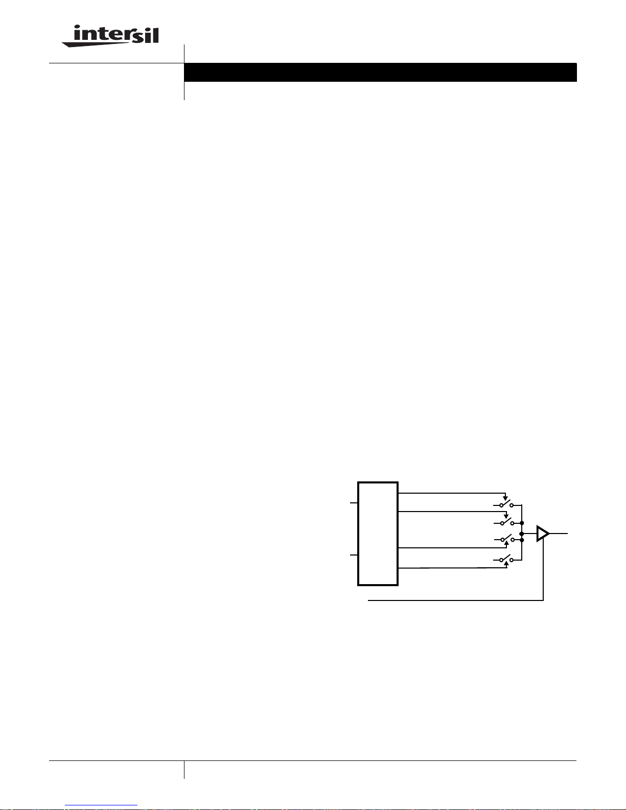
The ISL59442 is a single-output 4:1 MUX-amp. The output
amplifier unity-gain bandwidth is 1GHz. The device
contains logic inputs for channel selection (S0, S1), and a
three-state output control (HIZ) for individual selection of
MUX amps that share a common video output line.
The evaluation board circuit and layout is optimized for
either 50Ω or 75Ω terminations, and implements a basic
single 4:1 video MUX-amp. The board is supplied with 75Ω
input signal terminations and a 75Ω back-termination
resistor on each of the 3 outputs, making it suitable for
driving video cable. The user has the option of replacing the
75Ω resistors with 50Ω resistors for other applications. The
control lines contain 50Ω resistors to match the 50Ω output
impedance of high speed pulse generators. Control line
termination resistors are recommended for rise and fall times
under 10ns to minimize unwanted transients. If DC is used
for the control logic, the resistors may be removed; or the
applied DC voltage can be reduced to 2.5V to reduce the
dissipation in the termination resistor.
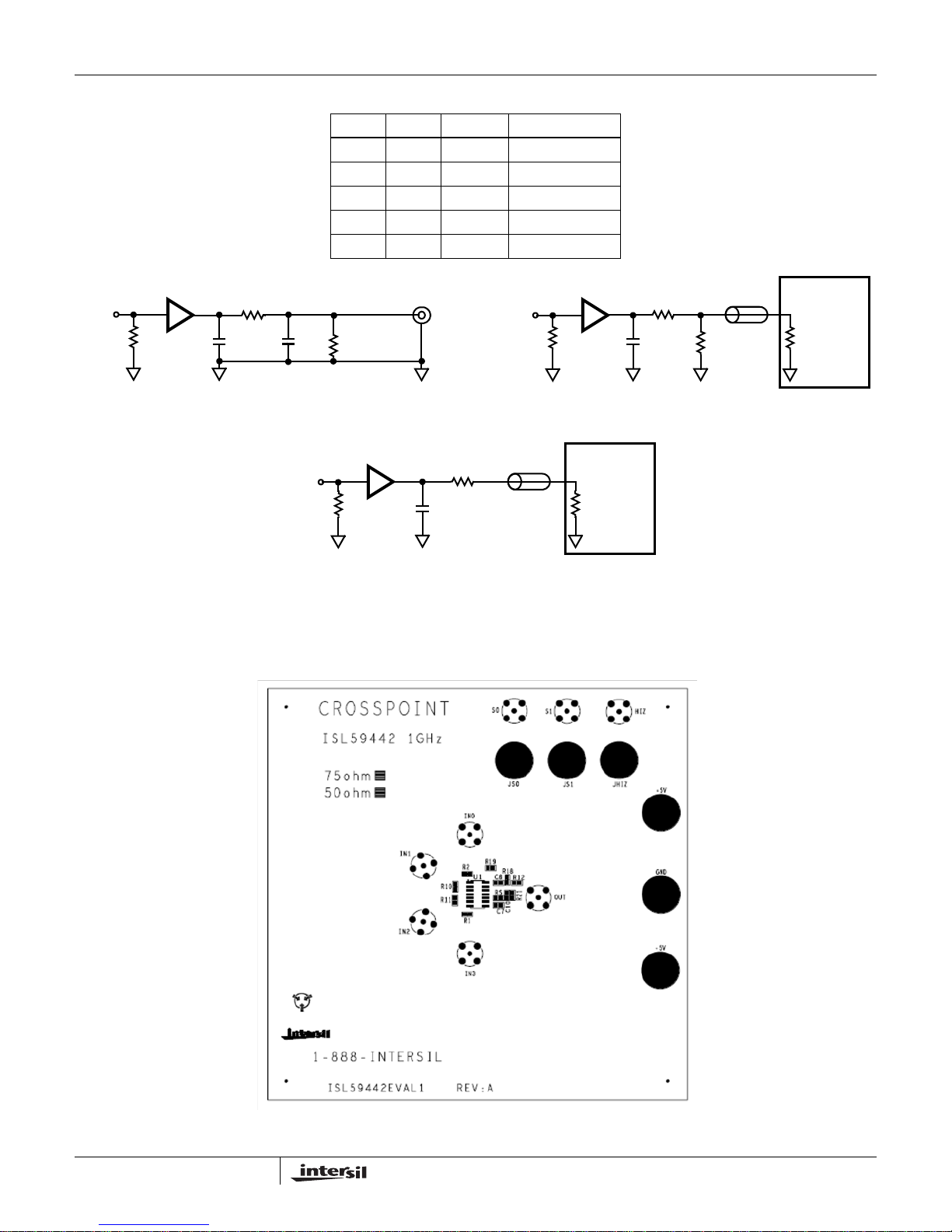
The layout contains component options to include an output
series resistor (R
capacitor (C
) followed by a parallel resistor (RL)
S
) network to ground. This option allows the user
L
to select several different output configurations. Examples
are shown in Figures 2A, 2B, and 2C. The evaluation board
is supplied with the 75Ω back termination resistors shown in
Figure 2C.
Amplifier Performance and Output
Configurations
The ISL59442 output amplifier is sensitive to capacitance at
the output. For best AC performance, a series output resistor
is required to reduce excessive gain peaking, particularly
when long PB board traces are used. The output amplifier is
ideally suited for driving high impedance high speed
selectable-gain buffers when gain compensation is needed.
GBW decreases slightly at the lower output load
impedances typical of back-terminated cable driving
applications. Reference data sheets for additional
performance data.
AN1185.0
High Frequency Layout Considerations
At frequencies of 500MHz and higher, circuit board layout
may limit performance. The following layout guidelines are
implemented on the evaluation board:
• Signal I/O lines are the same lengths and widths to match
propagation delay and trace parasitics.
• No series connected vias are used in signal I/O lines, as
they can add unwanted inductance.
• Signal trace lengths are minimized to reduce transmission
line effects and the need for strip-line tuning of the signal
traces.
• High frequency decoupling caps are placed as close to the
device power supply pin as possible - without series vias
between the capacitor and the device pin.
Power Sequencing
Proper power supply sequencing is -V first, then +V. In
addition, the +V and -V supply pin voltage rate-of-rise must
be limited to ±1V/µs or less. The evaluation board contains
parallel-connected low V
Schottky diodes on each supply
ON
terminal to minimize the risk of latch up due to incorrect
sequencing. In addition, extra 10µF decoupling capacitors
are added to each supply to aid in reducing the applied
voltage rate-of-rise.
Reference Documents
• ISL59442 Data Sheet, FN7452
EN0
S0
DECODE
S1
HIZ
FIGURE 1. ISL59442 FUNCTIONAL BLOCK DIAGRAM
EN1
EN2
EN3
IN0
IN1
IN2
IN3
OUT
1
CAUTION: These devices are sensitive to electrostatic discharge; follow proper IC Handling Procedures.
1-888-INTERSIL or 1-888-352-6832
| Intersil (and design) is a registered trademark of Intersil Americas Inc.
All other trademarks mentioned are the property of their respective owners.
Copyright Intersil Americas Inc. 2005. All Rights Reserved
Page 2
Application Note 1185
TAB L E 1 . LO G I C TA BLE
S0 S1 HIZ OUT
00 0 IN0
10 0 IN1
01 0 IN2
11 0 IN3
- - 1 High Z
ISL59442
V
IN
50Ω
OR
75Ω
RS, 0Ω
C
b1
~0.5pF
*C
b2
~3pF
R
L
500Ω
* Cb1, Cb2 are approximate PCB trace capacitances.
FIGURE 2A. TEST CIRCUIT WITH OPTIMAL OUTPUT LOAD
ISL59442
V
IN
50Ω
OR
75Ω
is approximate PCB trace capacitance.
* C
b1
FIGURE 2C. BACK-TERMINATED TEST CIRCUIT FOR CABLE APPLICATION
ISL59442EVAL1 Top View
R
S
50Ω OR 75Ω
C
b1
~0.5pF
ISL59442
V
IN
50Ω
OR
75Ω
R
475Ω
C
b1
~0.5pF
S
50Ω
R
OR
L
75Ω
TEST
EQUIPMENT
50Ω
OR
75Ω
* Cb1 is approximate PCB trace capacitance.
FIGURE 2B. TEST CIRCUIT FOR 50Ω OR 75Ω TERMINATIONS
TEST
EQUIPMENT
50Ω
OR
75Ω
2
AN1185.0
April 19, 2005
Page 3
Application Note 1185
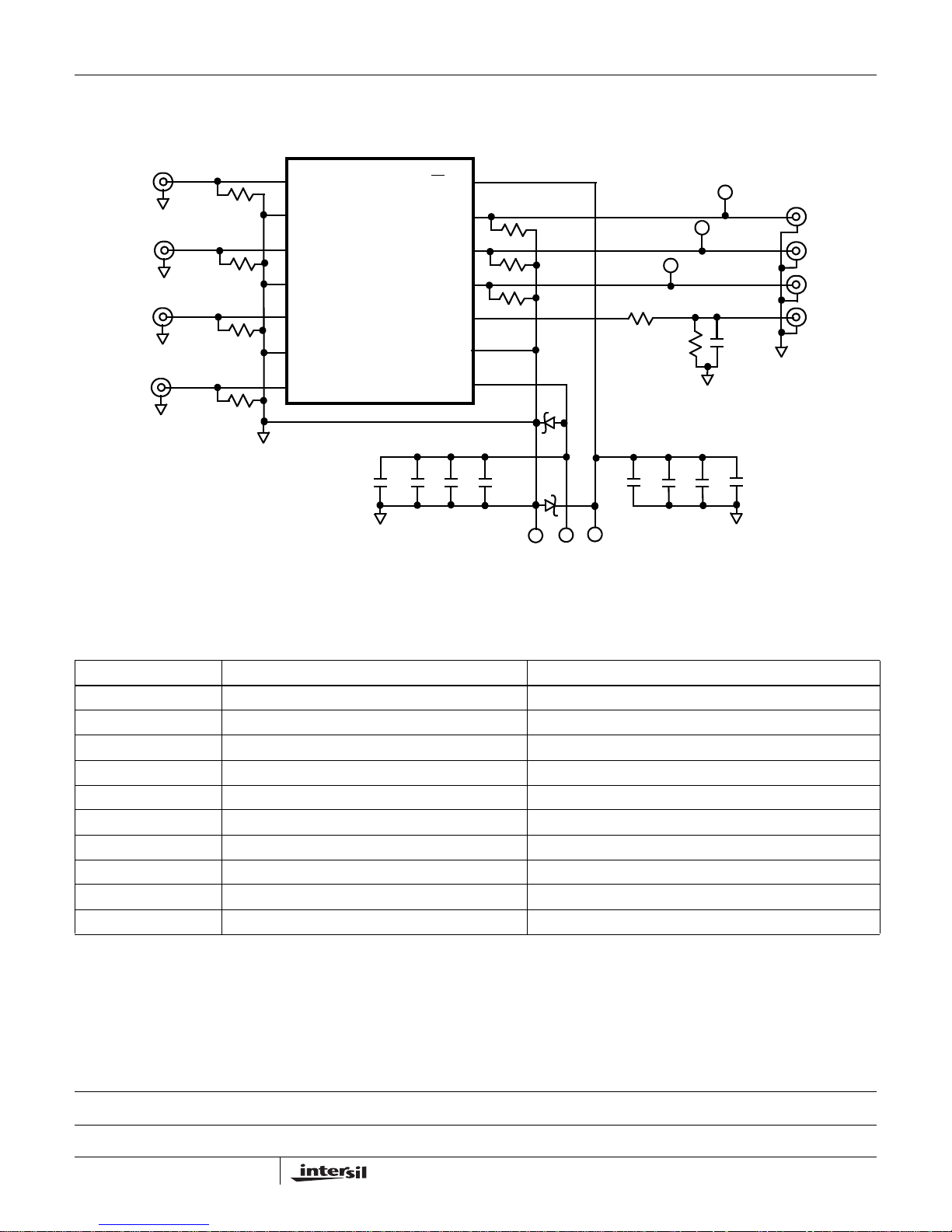
ISL59442EVAL1 Schematic Diagram
IN0
IN1
IN2
IN3
R2
75Ω
R10
75Ω
R11
75Ω
R1
75Ω
1 IN0
2 GND
3 IN1
4 GND
5 IN2
6 GND
7 IN3
ISL59442
C3
10µF
V+
S0 13
S1 12
HIZ 11
OUT 10
NIC 9
C2
0.1µFC110nF
14
V- 8
R19 - 49.9Ω
R18 - 49.9Ω
R12 - 49.9Ω
C7
1nF
JS0
JS1
JHIZ
RS - 75Ω
D1
+
+
D2
GND
C6
10µF
V+
V-
R21
C5
0.1µFC410nF
C10
C8
1nF
S0
S1
HIZ
OUT
ISL59442EVAL1 Components Parts List
DEVICE # DESCRIPTION COMMENTS
C7, C8 CAP, SMD, 0603, 1000pF, 25V, 10%, X7R Power Supply Decoupling
C1, C4 CAP, SMD, 0603, 0.01µF, 25V, 10%, X7R Power Supply Decoupling
C2, C5 CAP, SMD, 0603, 0.1µF, 25V, 10%, X7R Power Supply Decoupling
C3, C6 CAP, SMD, 0805, 10µF, 6.3V, 10%, X5R Power Supply Decoupling
D1, D2 Diode-Schottky, 2 Pin, 45V, 7.5A MBR0550T (Motorola) Reverse Polarity Protection
R1, R2, R10, R11, RS Resistor, SMD, 0603, 75Ω, 1/10W, 1% Signal Input/output Termination
R12, R18, R19 Resistor, SMD, 0603, 49.9Ω, 1/16W, 1% Logic Input Termination
C10 Resistor, SMD, 0603 Optional, not populated
R21 Resistor, SMD, 0603 Optional, not populated
U1 ISL59442 - 1GHz Multiplexing Amplifier, 14P, QSOP Device Under Test
Intersil Corporation reserves the right to make changes in circuit design, software and/or specifications at any time without notice. Accordingly, the reader is cautioned to
verify that the Application Note or Technical Brief is current before proceeding.
For information regarding Intersil Corporation and its products, see www.intersil.com
3
AN1185.0
April 19, 2005
 Loading...